View fdms3602s detailed specification:

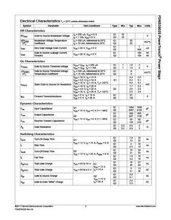
March 2011 FDMS3602S PowerTrench Power Stage Asymmetric Dual N-Channel MOSFET Features General Description Q1 N-Channel This device includes two specialized N-Channel MOSFETs in a dual PQFN package. The switch node has been internally Max rDS(on) = 5.6 m at VGS = 10 V, ID = 15 A connected to enable easy placement and routing of synchronous Max rDS(on) = 8.1 m at VGS = 4.5 V, ID = 14 A buck converters. The control MOSFET (Q1) and synchronous Q2 N-Channel SyncFET (Q2) have been designed to provide optimal power Max rDS(on) = 2.2 m at VGS = 10 V, ID = 26 A efficiency. Max rDS(on) = 3.4 m at VGS = 4.5 V, ID = 22 A Applications Low inductance packaging shortens rise/fall times, resulting in lower switching losses Computing MOSFET integration enables optimum layout for lower circuit Communications inductance and reduced switch node ringing ... See More ⇒
Keywords - ALL TRANSISTORS SPECS
fdms3602s.pdf Design, MOSFET, Power
fdms3602s.pdf RoHS Compliant, Service, Triacs, Semiconductor
fdms3602s.pdf Database, Innovation, IC, Electricity
BJT Parameters and How They Relate
🌐 : EN ES РУ

LIST
Last Update
BJT: ZDT6705 | GA1L4Z | GA1A4M | SBT42 | 2SA200-Y | 2SA200-O
Popular searches
irfz44n | irf3205 | irfz44n datasheet | 2n4401 | bc547 transistor | bd139 | 2n4401 datasheet