View j111 j112 j113 mmbfj111 mmbfj112 mmbfj113 detailed specification:

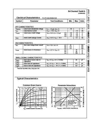
J111 MMBFJ111 J112 MMBFJ112 J113 MMBFJ113 G S G TO-92 S SOT-23 D D Mark 6P / 6R / 6S NOTE Source & Drain are interchangeable N-Channel Switch This device is designed for low level analog switching, sample and hold circuits and chopper stabilized amplifiers. Sourced from Process 51. Absolute Maximum Ratings* TA = 25 C unless otherwise noted Symbol Parameter Value Units VDG Drain-Gate Voltage 35 V VGS Gate-Source Voltage - 35 V 5 IGF Forward Gate Current 50 mA Operating and Storage Junction Temperature Range -55 to +150 C TJ ,Tstg *These ratings are limiting values above which the serviceability of any semiconductor device may be impaired. NOTES 1) These ratings are based on a maximum junction temperature of 150 degrees C. 2) These are steady state limits. The factory should be consulted on applications involving pulsed or low duty cycle operations. Th... See More ⇒
Keywords - ALL TRANSISTORS SPECS
j111 j112 j113 mmbfj111 mmbfj112 mmbfj113.pdf Design, MOSFET, Power
j111 j112 j113 mmbfj111 mmbfj112 mmbfj113.pdf RoHS Compliant, Service, Triacs, Semiconductor
j111 j112 j113 mmbfj111 mmbfj112 mmbfj113.pdf Database, Innovation, IC, Electricity
BJT Parameters and How They Relate
🌐 : EN ES РУ

LIST
Last Update
BJT: ZDT6705 | GA1L4Z | GA1A4M | SBT42 | 2SA200-Y | 2SA200-O
Popular searches
irfz44n | irf3205 | irfz44n datasheet | 2n4401 | bc547 transistor | bd139 | 2n4401 datasheet