View 2n3055 detailed specification:
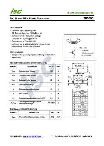
isc Silicon NPN Power Transistor 2N3055 DESCRIPTION Excellent Safe Operating Area DC Current Gain-h =20-70@I = 4A FE C Collector-Emitter Saturation Voltage- V )= 1.1 V(Max)@ I = 4A CE(sat C Complement to Type MJ2955 Minimum Lot-to-Lot variations for robust device performance and reliable operation APPLICATIONS Designed for general-purpose switching and amplifier applications ABSOLUTE MAXIMUM RATINGS(T =25 ) a SYMBOL PARAMETER VALUE UNIT V Collector-Base Voltage 100 V CBO V Collector-Emitter Voltage 70 V CER V Collector-Emitter Voltage 60 V CEO V Emitter-Base Voltage 7 V EBO I Collector Current-Continuous 15 A C I Base Current 7 A B P Collector Power Dissipation@T =25 115 W C C Operating and Storage Junction T T -65 +150 J, stg Temperature Range THERMAL CHARACTERISTICS SYMBOL PARAMETER MAX UNIT R Thermal Resistance,Junction to... See More ⇒
Keywords - ALL TRANSISTORS SPECS
2n3055.pdf Design, MOSFET, Power
2n3055.pdf RoHS Compliant, Service, Triacs, Semiconductor
2n3055.pdf Database, Innovation, IC, Electricity
BJT Parameters and How They Relate
🌐 : EN ES РУ

LIST
Last Update
BJT: ZDT6705 | GA1L4Z | GA1A4M | SBT42 | 2SA200-Y | 2SA200-O
Popular searches
irfz44n | irf3205 | irfz44n datasheet | 2n4401 | bc547 transistor | bd139 | 2n4401 datasheet