View 2sk3566 detailed specification:
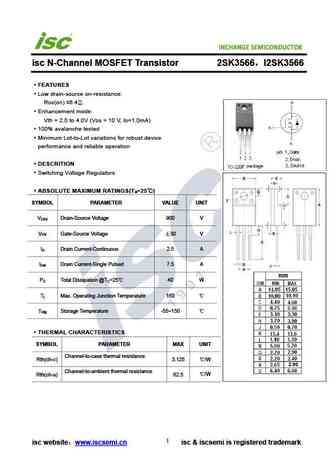
isc N-Channel MOSFET Transistor 2SK3566 I2SK3566 FEATURES Low drain-source on-resistance RDS(on) 6.4 . Enhancement mode Vth = 2.0 to 4.0V (VDS = 10 V, ID=1.0mA) 100% avalanche tested Minimum Lot-to-Lot variations for robust device performance and reliable operation DESCRITION Switching Voltage Regulators ABSOLUTE MAXIMUM RATINGS(T =25 ) a SYMBOL PARAMETER VALUE UNIT V Drain-Source Voltage 900 V DSS V Gate-Source Voltage 30 V GS I Drain Current-Continuous 2.5 A D I Drain Current-Single Pulsed 7.5 A DM P Total Dissipation @T =25 40 W D C T Max. Operating Junction Temperature 150 j Storage Temperature -55 150 T stg THERMAL CHARACTERISTICS SYMBOL PARAMETER MAX UNIT Channel-to-case thermal resistance /W Rth(ch-c) 3.125 Channel-to-ambient thermal resistance /W Rth(ch-a) 62.5 1 isc website www.iscsemi.cn ... See More ⇒
Keywords - ALL TRANSISTORS SPECS
2sk3566.pdf Design, MOSFET, Power
2sk3566.pdf RoHS Compliant, Service, Triacs, Semiconductor
2sk3566.pdf Database, Innovation, IC, Electricity
BJT Parameters and How They Relate
🌐 : EN ES РУ

LIST
Last Update
BJT: ZDT6705 | GA1L4Z | GA1A4M | SBT42 | 2SA200-Y | 2SA200-O
Popular searches
irfz44n | irf3205 | irfz44n datasheet | 2n4401 | bc547 transistor | bd139 | 2n4401 datasheet