View j111 j112 detailed specification:
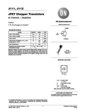
J111, J112 JFET Chopper Transistors N-Channel Depletion Features http //onsemi.com Pb-Free Packages are Available* 1 DRAIN MAXIMUM RATINGS Rating Symbol Value Unit 3 Drain-Gate Voltage VDG -35 Vdc GATE Gate -Source Voltage VGS -35 Vdc Gate Current IG 50 mAdc 2 SOURCE Total Device Dissipation @ TA = 25 C PD 350 mW Derate above = 25 C 2.8 mW/ C Lead Temperature TL 300 C Operating and Storage Junction TJ, Tstg -65 to +150 C Temperature Range Maximum ratings are those values beyond which device damage can occur. TO-92 Maximum ratings applied to the device are individual stress limit values (not CASE 29-11 normal operating conditions) and are not valid simultaneously. If these limits are 1 STYLE 5 exceeded, device functional operation is not implied, damage may occur and 2 3 reliability may be affected. MARKING DIAGRAM J11x AYWW G G J11x = ... See More ⇒
Keywords - ALL TRANSISTORS SPECS
j111 j112.pdf Design, MOSFET, Power
j111 j112.pdf RoHS Compliant, Service, Triacs, Semiconductor
j111 j112.pdf Database, Innovation, IC, Electricity
BJT Parameters and How They Relate
🌐 : EN ES РУ

LIST
Last Update
BJT: ZDT6705 | GA1L4Z | GA1A4M | SBT42 | 2SA200-Y | 2SA200-O
Popular searches
irfz44n | irf3205 | irfz44n datasheet | 2n4401 | bc547 transistor | bd139 | 2n4401 datasheet