View p2n2222a-d detailed specification:
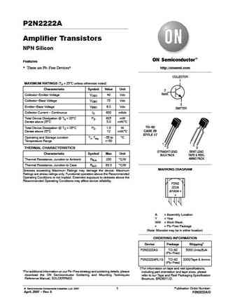
P2N2222A Amplifier Transistors NPN Silicon Features These are Pb--Free Devices* http //onsemi.com COLLECTOR 1 MAXIMUM RATINGS (TA =25 C unless otherwise noted) Characteristic Symbol Value Unit 2 BASE Collector--Emitter Voltage VCEO 40 Vdc Collector--Base Voltage VCBO 75 Vdc 3 Emitter--Base Voltage VEBO 6.0 Vdc EMITTER Collector Current -- Continuous IC 600 mAdc Total Device Dissipation @ TA =25 C PD 625 mW Derate above 25 C 5.0 mW/ C TO--92 Total Device Dissipation @ TC =25 C PD 1.5 W CASE 29 Derate above 25 C 12 mW/ C STYLE 17 Operating and Storage Junction TJ, Tstg --55 to C Temperature Range +150 1 1 2 2 3 THERMAL CHARACTERISTICS 3 STRAIGHT LEAD BENT LEAD Characteristic Symbol Max Unit BULK PACK TAPE & REEL AMMO PACK Thermal Resistance, Junction to Ambient R JA 200 C/W Thermal Resistance, Junction to Case R JC 83.3 C/W MARKI... See More ⇒
Keywords - ALL TRANSISTORS SPECS
p2n2222a-d.pdf Design, MOSFET, Power
p2n2222a-d.pdf RoHS Compliant, Service, Triacs, Semiconductor
p2n2222a-d.pdf Database, Innovation, IC, Electricity
BJT Parameters and How They Relate
🌐 : EN ES РУ

LIST
Last Update
BJT: ZDT6705 | GA1L4Z | GA1A4M | SBT42 | 2SA200-Y | 2SA200-O
Popular searches
irfz44n | irf3205 | irfz44n datasheet | 2n4401 | bc547 transistor | bd139 | 2n4401 datasheet