View 2sk2619 detailed specification:
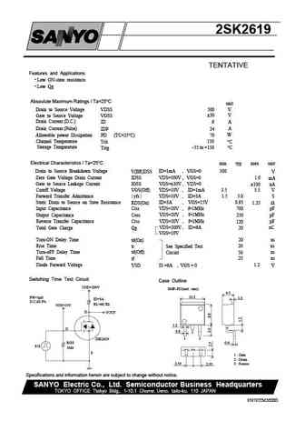
2SK2619 TENTATIVE Features and Applications Low ON-state resistance. Low Qg Absoulute Maximum Ratings / Ta=25 C unit Drain to Source Voltage VDSS 500 V 30 Gate to Source Voltage VGSS V Drain Current (D.C.) 6 A ID Drain Current (Pulse) A IDP 24 Allowable power Dissipation PD (TC=25 C) 70 W Channel Temperature 150 Tch C Storage Temperature Tstg --55 to +150 C Electrical Characteristics / Ta=25 C min typ max unit 500 Drain to Source Breakdown Voltage ID=1mA , VGS=0 V V(BR)DSS Zero Gate Voltage Drain Current IDSS VDS=500V , VGS=0 1.0 mA Gate to Source Leakage Current IGSS VGS= 30V , VDS=0 100 nA Cutoff Voltage VGS(Off) VDS=10V , ID=1mA 3.5 5.5 V Forward Transfer Admittance yfs VDS=10V , ID=3A 1.5 3.0 S Static Drain to Source on State Resistance RDS(On) ID=3A , VGS=15V 0.95 1.25 Input Capacitance Ciss VDS=20V , f=1MHz 700 pF ... See More ⇒
Keywords - ALL TRANSISTORS SPECS
2sk2619.pdf Design, MOSFET, Power
2sk2619.pdf RoHS Compliant, Service, Triacs, Semiconductor
2sk2619.pdf Database, Innovation, IC, Electricity
BJT Parameters and How They Relate
🌐 : EN ES РУ

LIST
Last Update
BJT: ZDT6705 | GA1L4Z | GA1A4M | SBT42 | 2SA200-Y | 2SA200-O
Popular searches
irfz44n | irf3205 | irfz44n datasheet | 2n4401 | bc547 transistor | bd139 | 2n4401 datasheet