View csd16327q3 detailed specification:
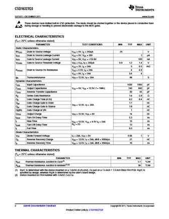
CSD16327Q3 www.ti.com SLPS371 DECEMBER 2011 N-Channel NexFET Power MOSFET Check for Samples CSD16327Q3 1 FEATURES PRODUCT SUMMARY 2 Optimized for 5V Gate Drive VDS Drain to Source Voltage 25 V Ultra Low Qg and Qgd Qg Gate Charge Total (4.5V) 6.2 nC Low Thermal Resistance Qgd Gate Charge Gate to Drain 1.1 nC VGS = 3V 5 m Avalanche Rated RDS(on) Drain to Source On Resistance VGS = 4.5V 4 Pb Free Terminal Plating VGS = 8V 3.4 RoHS Compliant Vth Threshold Voltage 1.2 V Halogen Free SON 3.3mm x 3.3mm Plastic Package ORDERING INFORMATION Device Package Media Qty Ship APPLICATIONS SON 3.3 3.3 13-inch Tape and CSD16327Q3 2500 Plastic Package reel Reel Point-of-Load Synchronous Buck Converter for Applications in Networking, Telecom and ABSOLUTE MAXIMUM RATINGS Computing Systems TA = 25 C unless otherwise stated ... See More ⇒
Keywords - ALL TRANSISTORS SPECS
csd16327q3.pdf Design, MOSFET, Power
csd16327q3.pdf RoHS Compliant, Service, Triacs, Semiconductor
csd16327q3.pdf Database, Innovation, IC, Electricity
BJT Parameters and How They Relate
🌐 : EN ES РУ

LIST
Last Update
BJT: ZDT6705 | GA1L4Z | GA1A4M | SBT42 | 2SA200-Y | 2SA200-O
Popular searches
irfz44n | irf3205 | irfz44n datasheet | 2n4401 | bc547 transistor | bd139 | 2n4401 datasheet