View ixtk102n30p datasheet:
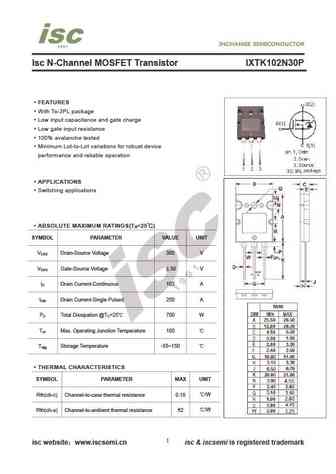
Isc N-Channel MOSFET Transistor IXTK102N30PFEATURESWith To-3PL packageLow input capacitance and gate chargeLow gate input resistance100% avalanche testedMinimum Lot-to-Lot variations for robust deviceperformance and reliable operationAPPLICATIONSSwitching applicationsABSOLUTE MAXIMUM RATINGS(T =25)aSYMBOL PARAMETER VALUE UNITV Drain-Source Voltage 300 VDSSV Gate-Source Voltage 30 VGSSI Drain Current-Continuous 102 ADI Drain Current-Single Pulsed 250 ADMP Total Dissipation @T =25 700 WD CT Max. Operating Junction Temperature 150 chStorage Temperature -55~150 TstgTHERMAL CHARACTERISTICSSYMBOL PARAMETER MAX UNIT/WRth(ch-c) Channel-to-case thermal resistance 0.18/WRth(ch-a) Channel-to-ambient thermal resistance 621isc websitewww.iscsemi.cn isc & iscsemi is registered trademark
Keywords - ALL TRANSISTORS DATASHEET
ixtk102n30p.pdf Design, MOSFET, Power
ixtk102n30p.pdf RoHS Compliant, Service, Triacs, Semiconductor
ixtk102n30p.pdf Database, Innovation, IC, Electricity


LIST
Last Update
BJT: GA1A4M | SBT42 | 2SA200-Y | 2SA200-O | 2SD882-Q | 2SD882-P | 2SD882-E | 2SC945-L | 2SC945-H | 2SC4226-R23 | 2SC3357-F | 2SC3357-E | 2SC3356-R26 | 2SC3356-R24 | 2SC3356-R23 | 2SB772-Q | 2SB772-P | 2SB772-E | 2SA1015-L | 2SA1015-H | HSS8550
Popular searches
irfz44n | irf3205 | irfz44n datasheet | 2n4401 | bc547 transistor | bd139 | 2n4401 datasheet