2n5484 mmbf5484.pdf Principales características:
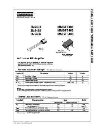
2N5484 MMBF5484 2N5485 MMBF5485 2N5486 MMBF5486 G S G TO-92 S SOT-23 D D Mark 6B / 6M / 6H NOTE Source & Drain are interchangeable N-Channel RF Amplifier This device is designed primarily for electronic switching applications such as low On Resistance analog switching. Sourced from Process 50. Absolute Maximum Ratings* TA = 25 C unless otherwise noted Symbol Parameter Value Units VDG Drain-Gate Voltage 25 V VGS Gate-Source Voltage - 25 V IGF Forward Gate Current 10 mA Operating and Storage Junction Temperature Range -55 to +150 C TJ ,Tstg *These ratings are limiting values above which the serviceability of any semiconductor device may be impaired. NOTES 1) These ratings are based on a maximum junction temperature of 150 degrees C. 2) These are steady state limits. The factory should be consulted on applications involving pulsed or low duty cycle opera... MOSTRAR MÁS ⇒
Keywords - ALL TRANSISTORS. Principales características
2n5484 mmbf5484.pdf Design, MOSFET, Power
2n5484 mmbf5484.pdf RoHS Compliant, Service, Triacs, Semiconductor
2n5484 mmbf5484.pdf Database, Innovation, IC, Electricity
Parámetros del transistor bipolar y su interrelación.
🌐 : EN ES РУ

Liste
Recientemente añadidas las descripciónes de los transistores:
BJT: ZDT6705 | GA1L4Z | GA1A4M | SBT42 | 2SA200-Y | 2SA200-O | 2SD882-Q | 2SD882-P | 2SD882-E | 2SC945-L | 2SC945-H | 2SC4226-R23 | 2SC3357-F | 2SC3357-E | 2SC3356-R26 | 2SC3356-R24 | 2SC3356-R23 | 2SB772-Q | 2SB772-P | 2SB772-E | 2SA1015-L
Popular searches
irfz44n | irf3205 | irfz44n datasheet | 2n4401 | bc547 transistor | bd139 | 2n4401 datasheet