nvtfs6h888n.pdf Principales características:
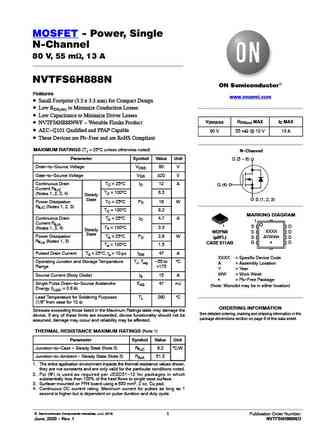
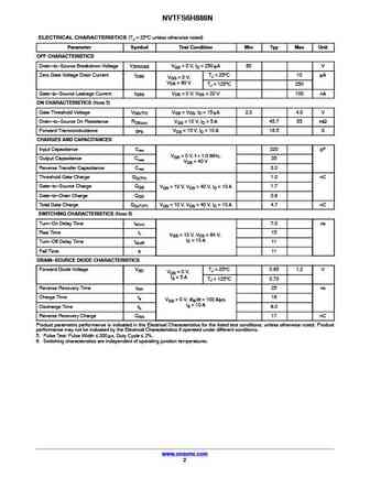
MOSFET - Power, Single N-Channel 80 V, 55 mW, 13 A NVTFS6H888N Features www.onsemi.com Small Footprint (3.3 x 3.3 mm) for Compact Design Low RDS(on) to Minimize Conduction Losses Low Capacitance to Minimize Driver Losses V(BR)DSS RDS(on) MAX ID MAX NVTFS6H888NWF - Wettable Flanks Product AEC-Q101 Qualified and PPAP Capable 80 V 55 mW @ 10 V 13 A These Devices are Pb-Free and are RoHS Compliant MAXIMUM RATINGS (TJ = 25 C unless otherwise noted) N-Channel Parameter Symbol Value Unit D (5 - 8) Drain-to-Source Voltage VDSS 80 V Gate-to-Source Voltage VGS 20 V Continuous Drain TC = 25 C ID 12 A G (4) Current RqJC TC = 100 C 8.3 (Notes 1, 2, 3, 4) Steady State S (1, 2, 3) Power Dissipation TC = 25 C PD 18 W RqJC (Notes 1, 2, 3) TC = 100 C 9.2 MARKING DIAGRAM Continuous Drain TA = 25 C ID 4.7 A 1 Current RqJA 1 S D TA = 10
Keywords - ALL TRANSISTORS. Principales características
nvtfs6h888n.pdf Design, MOSFET, Power
nvtfs6h888n.pdf RoHS Compliant, Service, Triacs, Semiconductor
nvtfs6h888n.pdf Database, Innovation, IC, Electricity
Parámetros del transistor bipolar y su interrelación.
🌐 : EN ES РУ

Liste
Recientemente añadidas las descripciónes de los transistores:
BJT: GA1A4M | SBT42 | 2SA200-Y | 2SA200-O | 2SD882-Q | 2SD882-P | 2SD882-E | 2SC945-L | 2SC945-H | 2SC4226-R23 | 2SC3357-F | 2SC3357-E | 2SC3356-R26 | 2SC3356-R24 | 2SC3356-R23 | 2SB772-Q | 2SB772-P | 2SB772-E | 2SA1015-L | 2SA1015-H | HSS8550
Popular searches
irfz44n | irf3205 | irfz44n datasheet | 2n4401 | bc547 transistor | bd139 | 2n4401 datasheet