rjp30h2dpk-m0 rjp30h2a.pdf Principales características:
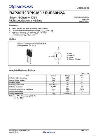
Preliminary Datasheet RJP30H2DPK-M0 / RJP30H2A R07DS0467EJ0200 Silicon N Channel IGBT Rev.2.00 High speed power switching Jun 15, 2011 Features Trench gate and thin wafer technology (G6H-II series) Low collector to emitter saturation voltage VCE(sat) = 1.4 V typ High speed switching tf = 100 ns typ, tf = 180 ns typ Low leak current ICES = 1 A max Outline RENESAS Package code PRSS0004ZH-A (Package name TO-3PSG) C 4 1. Gate 2. Collector G 3. Emitter 4. Collector (Flange) 1 2 3 E Absolute Maximum Ratings www.DataSheet.co.kr (Ta = 25 C) Item Symbol Ratings Unit Collector to Emitter voltage VCES 360 V Gate to Emitter voltage VGES 30 V Collector current Ic 35 A Collector peak current ic(peak) Note1 250 A Collector dissipation PC Note2 60 W Junction to case thermal impedance j-c 2.08 C/ W Junction temperature Tj 150
Keywords - ALL TRANSISTORS. Principales características
rjp30h2dpk-m0 rjp30h2a.pdf Design, MOSFET, Power
rjp30h2dpk-m0 rjp30h2a.pdf RoHS Compliant, Service, Triacs, Semiconductor
rjp30h2dpk-m0 rjp30h2a.pdf Database, Innovation, IC, Electricity
Parámetros del transistor bipolar y su interrelación.
🌐 : EN ES РУ

Liste
Recientemente añadidas las descripciónes de los transistores:
BJT: ZDT6705 | GA1L4Z | GA1A4M | SBT42 | 2SA200-Y | 2SA200-O | 2SD882-Q | 2SD882-P | 2SD882-E | 2SC945-L | 2SC945-H | 2SC4226-R23 | 2SC3357-F | 2SC3357-E | 2SC3356-R26 | 2SC3356-R24 | 2SC3356-R23 | 2SB772-Q | 2SB772-P | 2SB772-E | 2SA1015-L
Popular searches
irfz44n | irf3205 | irfz44n datasheet | 2n4401 | bc547 transistor | bd139 | 2n4401 datasheet