p1504eis.pdf Principales características:
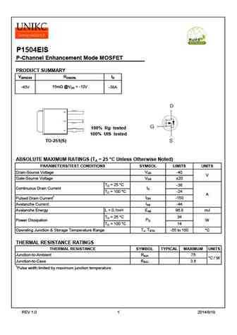
P1504EIS P-Channel Enhancement Mode MOSFET PRODUCT SUMMARY V(BR)DSS RDS(ON) ID 15m @VGS = -10V -40V -38A 100% Rg tested 100% UIS tested TO-251(S) ABSOLUTE MAXIMUM RATINGS (TA = 25 C Unless Otherwise Noted) PARAMETERS/TEST CONDITIONS SYMBOL LIMITS UNITS VDS Drain-Source Voltage -40 V VGS Gate-Source Voltage 20 TC = 25 C -38 ID Continuous Drain Current TC = 100 C -24 A IDM -150 Pulsed Drain Current1 IAS Avalanche Current -44 EAS Avalanche Energy L = 0.1mH 96.8 mJ TC = 25 C 34 PD Power Dissipation W TC = 100 C 14 TJ, TSTG Operating Junction & Storage Temperature Range -55 to 150 C THERMAL RESISTANCE RATINGS THERMAL RESISTANCE SYMBOL TYPICAL MAXIMUM UNITS Junction-to-Ambient RqJA 75 C / W Junction-to-Case RqJC 3.6 1 Pulse width limited by maximum junction temperature. REV 1.0 1 2014/8/18 P1504EIS P-Channel Enhan
Keywords - ALL TRANSISTORS. Principales características
p1504eis.pdf Design, MOSFET, Power
p1504eis.pdf RoHS Compliant, Service, Triacs, Semiconductor
p1504eis.pdf Database, Innovation, IC, Electricity
Parámetros del transistor bipolar y su interrelación.
🌐 : EN ES РУ

Liste
Recientemente añadidas las descripciónes de los transistores:
BJT: ZDT6705 | GA1L4Z | GA1A4M | SBT42 | 2SA200-Y | 2SA200-O | 2SD882-Q | 2SD882-P | 2SD882-E | 2SC945-L | 2SC945-H | 2SC4226-R23 | 2SC3357-F | 2SC3357-E | 2SC3356-R26 | 2SC3356-R24 | 2SC3356-R23 | 2SB772-Q | 2SB772-P | 2SB772-E | 2SA1015-L
Popular searches
irfz44n | irf3205 | irfz44n datasheet | 2n4401 | bc547 transistor | bd139 | 2n4401 datasheet