APT10M25BVFR MOSFET Equivalente. Reemplazo. Hoja de especificaciones. Principales características
Número de Parte: APT10M25BVFR
Tipo de FET: MOSFET
Polaridad de transistor: N
ESPECIFICACIONES MÁXIMAS
Pdⓘ - Máxima disipación de potencia: 300 W
|Vds|ⓘ - Voltaje máximo drenador-fuente: 100 V
|Vgs|ⓘ - Voltaje máximo fuente-puerta: 30 V
|Id|ⓘ - Corriente continua de drenaje: 75 A
Tjⓘ - Temperatura máxima de unión: 150 °C
CARACTERÍSTICAS ELÉCTRICAS
trⓘ - Tiempo de subida: 22 nS
Cossⓘ - Capacitancia de salida: 1600 pF
RDSonⓘ - Resistencia estado encendido drenaje a fuente: 0.025 Ohm
Encapsulados: TO247
Búsqueda de reemplazo de APT10M25BVFR MOSFET
- Selecciónⓘ de transistores por parámetros
APT10M25BVFR datasheet
apt10m25bvfr.pdf

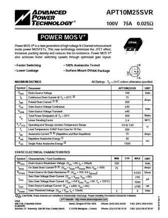
APT10M25BVFR 100V 75A 0.025 POWER MOS V FREDFET Power MOS V is a new generation of high voltage N-Channel enhancement TO-247 mode power MOSFETs. This new technology minimizes the JFET effect, increases packing density and reduces the on-resistance. Power MOS V also achieves faster switching speeds through optimized gate layout. Fast Recovery Body Diode 100% Avalanche Tes
apt10m25bvr.pdf

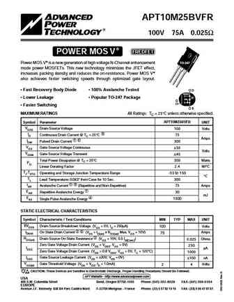
APT10M25BVR 100V 75A 0.025 POWER MOS V Power MOS V is a new generation of high voltage N-Channel enhancement TO-247 mode power MOSFETs. This new technology minimizes the JFET effect, increases packing density and reduces the on-resistance. Power MOS V also achieves faster switching speeds through optimized gate layout. D Faster Switching 100% Avalanche Tested Lower
apt10m25bvr.pdf
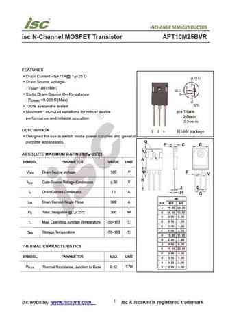
isc N-Channel MOSFET Transistor APT10M25BVR FEATURES Drain Current I =75A@ T =25 D C Drain Source Voltage- V =100V(Min) DSS Static Drain-Source On-Resistance R =0.025 (Max) DS(on) 100% avalanche tested Minimum Lot-to-Lot variations for robust device performance and reliable operation DESCRIPTION Designed for use in switch mode power supplies and general pur
apt10m25svr.pdf
APT10M25SVR 100V 75A 0.025 POWER MOS V D3PAK Power MOS V is a new generation of high voltage N-Channel enhancement mode power MOSFETs. This new technology minimizes the JFET effect, increases packing density and reduces the on-resistance. Power MOS V also achieves faster switching speeds through optimized gate layout. D Faster Switching 100% Avalanche Tested Lower
Otros transistores... APT10088HVR, APT10M07JVR, APT10M11B2VR, APT10M11JVR, APT10M11LVR, APT10M19BVFR, APT10M19BVR, APT10M19SVR, 75N75, APT10M25BVR, APT10M25SVR, APT1201R5BVR, APT1201R6BVR, APT12040JVR, APT12080JVR, APT12080LVR, APT20M11JVFR
History: IPI80N04S3-03
🌐 : EN ES РУ

Liste
Recientemente añadidas las descripciónes de los transistores:
MOSFET: CM4407 | CM3407 | CM3400 | SVF11N65F | SVF11N65T | FKBB3105 | EHBA036R1 | CRTT067N10N | AP6NA3R2MT | AP65SA145DDT8 | AP4NAR95CMT-A | AP4024GEMT-HF | AP3P050AH | AP3P020H | AP3N9R5YT | AP3N9R5MT
Popular searches
mje15030 | 2n3904 transistor | 2sd424 | 2sc828 | 2n4125 | tip42c transistor | c1815 transistor datasheet | mj15003