APT20M26WVR MOSFET Equivalente. Reemplazo. Hoja de especificaciones. Principales características
Número de Parte: APT20M26WVR
Tipo de FET: MOSFET
Polaridad de transistor: N
ESPECIFICACIONES MÁXIMAS
Pdⓘ - Máxima
disipación de potencia: 450 W
|Vds|ⓘ - Voltaje máximo drenador-fuente: 200 V
|Vgs|ⓘ - Voltaje máximo fuente-puerta: 30 V
|Id|ⓘ - Corriente continua
de drenaje: 65 A
Tjⓘ - Temperatura máxima de unión: 150 °C
CARACTERÍSTICAS ELÉCTRICAS
trⓘ - Tiempo
de subida: 25 nS
Cossⓘ - Capacitancia de salida: 1950 pF
RDSonⓘ - Resistencia estado encendido drenaje a fuente: 0.026 Ohm
Encapsulados: TO267
Búsqueda de reemplazo de APT20M26WVR MOSFET
- Selecciónⓘ de transistores por parámetros
APT20M26WVR datasheet
..1. Size:63K apt
apt20m26wvr.pdf 
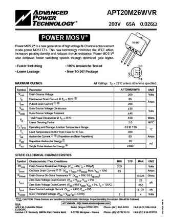
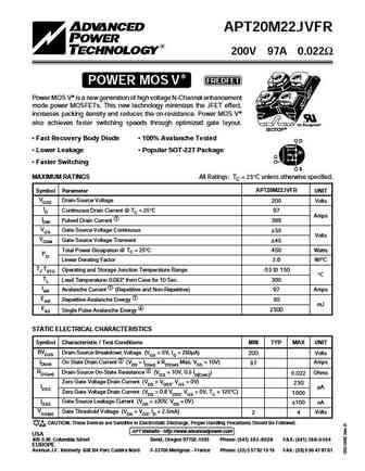
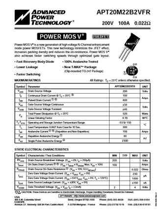
APT20M26WVR 200V 65A 0.026 POWER MOS V TO-267 Power MOS V is a new generation of high voltage N-Channel enhancement mode power MOSFETs. This new technology minimizes the JFET effect, increases packing density and reduces the on-resistance. Power MOS V also achieves faster switching speeds through optimized gate layout. Faster Switching 100% Avalanche Tested D Lower
7.1. Size:66K apt
apt20m22lvfr.pdf
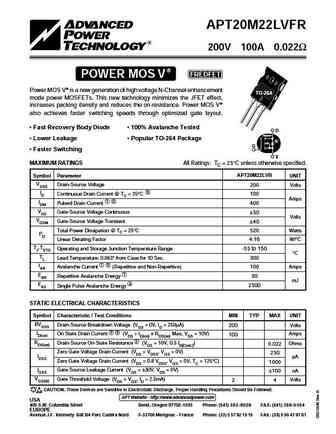
APT20M22LVFR 200V 100A 0.022 POWER MOS V FREDFET Power MOS V is a new generation of high voltage N-Channel enhancement TO-264 mode power MOSFETs. This new technology minimizes the JFET effect, increases packing density and reduces the on-resistance. Power MOS V also achieves faster switching speeds through optimized gate layout. Fast Recovery Body Diode 100% Avalanche T
7.2. Size:71K apt
apt20m22jvr.pdf
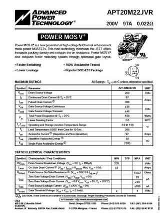
APT20M22JVR 200V 97A 0.022 POWER MOS V Power MOS V is a new generation of high voltage N-Channel enhancement mode power MOSFETs. This new technology minimizes the JFET effect, increases packing density and reduces the on-resistance. Power MOS V also achieves faster switching speeds through optimized gate layout. "UL Recognized" ISOTOP Faster Switching 100% Avalanche
7.3. Size:71K apt
apt20m22.pdf

APT20M22JVR 200V 97A 0.022 POWER MOS V Power MOS V is a new generation of high voltage N-Channel enhancement mode power MOSFETs. This new technology minimizes the JFET effect, increases packing density and reduces the on-resistance. Power MOS V also achieves faster switching speeds through optimized gate layout. "UL Recognized" ISOTOP Faster Switching 100% Avalanche
7.4. Size:71K apt
apt20m20b2fll.pdf
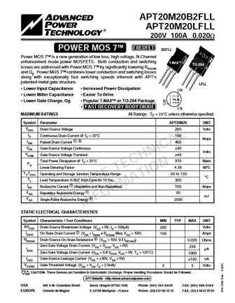
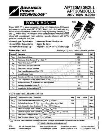
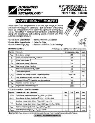
APT20M20B2FLL APT20M20LFLL 200V 100A 0.020W TM FREDFET POWER MOS 7 B2FLL Power MOS 7TM is a new generation of low loss, high voltage, N-Channel enhancement mode power MOSFETS. Both conduction and switching T-MAX TO-264 losses are addressed with Power MOS 7TM by significantly lowering RDS(ON) and Qg. Power MOS 7TM combines lower conduction and switching losses along with excepti
7.5. Size:157K apt
apt20m20b2fllg apt20m20lfllg.pdf
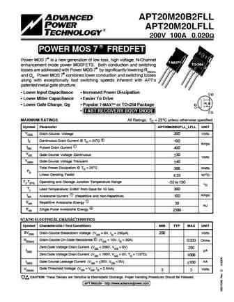
APT20M20B2FLL APT20M20LFLL 200V 100A 0.020 R FREDFET POWER MOS 7 FREDFET Power MOS 7 is a new generation of low loss, high voltage, N-Channel T-MAX TO-264 enhancement mode power MOSFETS. Both conduction and switching losses are addressed with Power MOS 7 by significantly lowering RDS(ON) and Qg. Power MOS 7 combines lower conduction and switching loss
7.6. Size:69K apt
apt20m20b2ll.pdf
APT20M20B2LL APT20M20LLL 200V 100A 0.020W B2LL TM POWER MOS 7 Power MOS 7TM is a new generation of low loss, high voltage, N-Channel T-MAX TO-264 enhancement mode power MOSFETS. Both conduction and switching losses are addressed with Power MOS 7TM by significantly lowering RDS(ON) and Qg. Power MOS 7TM combines lower conduction and switching losses along with exceptionally fast
7.7. Size:64K apt
apt20m22b2vfr.pdf
APT20M22B2VFR 200V 100A 0.022 POWER MOS V FREDFET T-MAX Power MOS V is a new generation of high voltage N-Channel enhancement mode power MOSFETs. This new technology minimizes the JFET effect, increases packing density and reduces the on-resistance. Power MOS V also achieves faster switching speeds through optimized gate layout. Fast Recovery Body Diode 100% Avalanch
7.9. Size:160K apt
apt20m20b2llg apt20m20lllg.pdf
APT20M20B2LL APT20M20LLL 200V 100A 0.020 R POWER MOS 7 MOSFET T-MAX Power MOS 7 is a new generation of low loss, high voltage, N-Channel TO-264 enhancement mode power MOSFETS. Both conduction and switching losses are addressed with Power MOS 7 by significantly lowering RDS(ON) and Qg. Power MOS 7 combines lower conduction and switching losses along wi
7.10. Size:60K apt
apt20m20jll.pdf
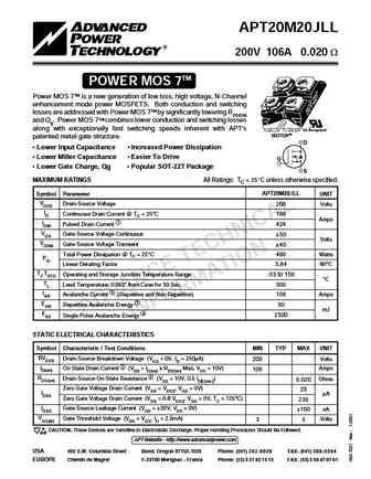
APT20M20JLL 200V 106A 0.020 W TM POWER MOS 7 Power MOS 7TM is a new generation of low loss, high voltage, N-Channel enhancement mode power MOSFETS. Both conduction and switching losses are addressed with Power MOS 7TM by significantly lowering RDS(ON) and Qg. Power MOS 7TM combines lower conduction and switching losses along with exceptionally fast switching speeds inherent with APT's
7.11. Size:63K apt
apt20m22b2vr.pdf
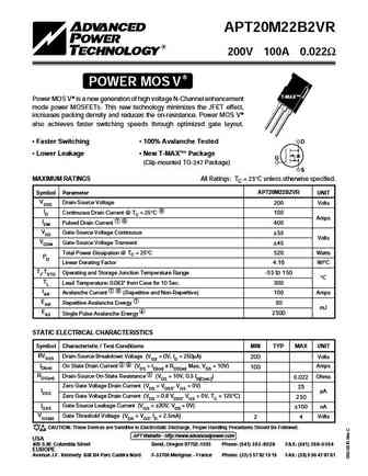
APT20M22B2VR 200V 100A 0.022 POWER MOS V T-MAX Power MOS V is a new generation of high voltage N-Channel enhancement mode power MOSFETs. This new technology minimizes the JFET effect, increases packing density and reduces the on-resistance. Power MOS V also achieves faster switching speeds through optimized gate layout. Faster Switching 100% Avalanche Tested D L
7.12. Size:64K apt
apt20m22lvr.pdf
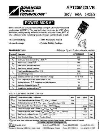
APT20M22LVR 200V 100A 0.022 POWER MOS V Power MOS V is a new generation of high voltage N-Channel enhancement TO-264 mode power MOSFETs. This new technology minimizes the JFET effect, increases packing density and reduces the on-resistance. Power MOS V also achieves faster switching speeds through optimized gate layout.. Faster Switching 100% Avalanche Tested D Low
7.13. Size:62K apt
apt20m20jfll.pdf
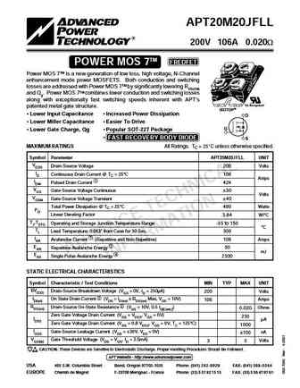
APT20M20JFLL 200V 106A 0.020W TM FREDFET POWER MOS 7 Power MOS 7TM is a new generation of low loss, high voltage, N-Channel enhancement mode power MOSFETS. Both conduction and switching losses are addressed with Power MOS 7TM by significantly lowering RDS(ON) and Qg. Power MOS 7TM combines lower conduction and switching losses along with exceptionally fast switching speeds inherent wi
7.14. Size:254K inchange semiconductor
apt20m22lvfr.pdf
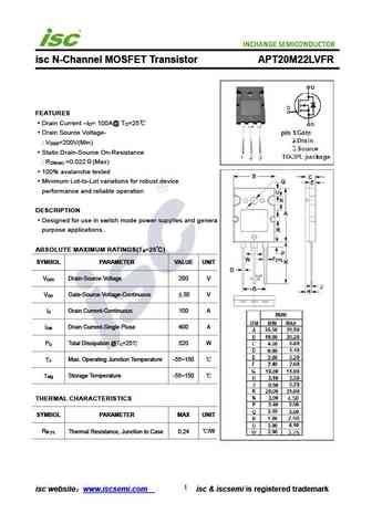
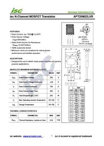
isc N-Channel MOSFET Transistor APT20M22LVFR FEATURES Drain Current I = 100A@ T =25 D C Drain Source Voltage- V =200V(Min) DSS Static Drain-Source On-Resistance R =0.022 (Max) DS(on) 100% avalanche tested Minimum Lot-to-Lot variations for robust device performance and reliable operation DESCRIPTION Designed for use in switch mode power supplies and general
7.15. Size:254K inchange semiconductor
apt20m20lfll.pdf
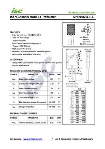
isc N-Channel MOSFET Transistor APT20M20LFLL FEATURES Drain Current I = 100A@ T =25 D C Drain Source Voltage- V =200V(Min) DSS Static Drain-Source On-Resistance R =0.02 (Max) DS(on) 100% avalanche tested Minimum Lot-to-Lot variations for robust device performance and reliable operation DESCRIPTION Designed for use in switch mode power supplies and general p
7.16. Size:375K inchange semiconductor
apt20m20b2fll.pdf
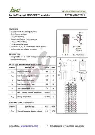
isc N-Channel MOSFET Transistor APT20M20B2FLL FEATURES Drain Current I = 100A@ T =25 D C Drain Source Voltage- V =200V(Min) DSS Static Drain-Source On-Resistance R =0.02 (Max) DS(on) 100% avalanche tested Minimum Lot-to-Lot variations for robust device performance and reliable operation DESCRIPTION Designed for use in switch mode power supplies and general
7.17. Size:375K inchange semiconductor
apt20m20b2ll.pdf
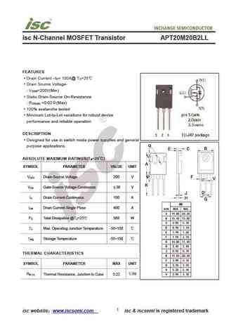
isc N-Channel MOSFET Transistor APT20M20B2LL FEATURES Drain Current I = 100A@ T =25 D C Drain Source Voltage- V =200V(Min) DSS Static Drain-Source On-Resistance R =0.02 (Max) DS(on) 100% avalanche tested Minimum Lot-to-Lot variations for robust device performance and reliable operation DESCRIPTION Designed for use in switch mode power supplies and general p
7.18. Size:254K inchange semiconductor
apt20m22lvr.pdf
isc N-Channel MOSFET Transistor APT20M22LVR FEATURES Drain Current I = 100A@ T =25 D C Drain Source Voltage- V =200V(Min) DSS Static Drain-Source On-Resistance R =0.022 (Max) DS(on) 100% avalanche tested Minimum Lot-to-Lot variations for robust device performance and reliable operation DESCRIPTION Designed for use in switch mode power supplies and general p
Otros transistores... APT20M13PVR, APT20M19JVR, APT20M22B2VFR, APT20M22B2VR, APT20M22JVFR, APT20M22JVR, APT20M22LVFR, APT20M22LVR, AO4407A, APT20M38BVFR, APT20M38BVR, APT20M38SVR, APT20M40BVR, APT20M42HVR, APT20M45BVFR, APT20M45BVR, APT20M45SVFR