APT5015BVR MOSFET Equivalente. Reemplazo. Hoja de especificaciones. Principales características
Número de Parte: APT5015BVR
Tipo de FET: MOSFET
Polaridad de transistor: N
ESPECIFICACIONES MÁXIMAS
Pdⓘ - Máxima disipación de potencia: 370 W
|Vds|ⓘ - Voltaje máximo drenador-fuente: 500 V
|Vgs|ⓘ - Voltaje máximo fuente-puerta: 30 V
|Id|ⓘ - Corriente continua de drenaje: 32 A
Tjⓘ - Temperatura máxima de unión: 150 °C
CARACTERÍSTICAS ELÉCTRICAS
trⓘ - Tiempo de subida: 14 nS
Cossⓘ - Capacitancia de salida: 600 pF
RDSonⓘ - Resistencia estado encendido drenaje a fuente: 0.15 Ohm
Encapsulados: TO247
Búsqueda de reemplazo de APT5015BVR MOSFET
- Selecciónⓘ de transistores por parámetros
APT5015BVR datasheet
apt5015bvr.pdf
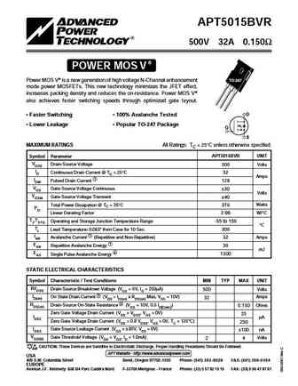
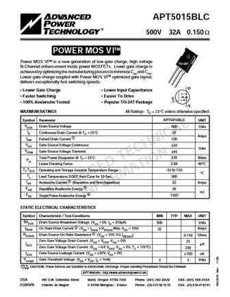
APT5015BVR 500V 32A 0.150 POWER MOS V Power MOS V is a new generation of high voltage N-Channel enhancement TO-247 mode power MOSFETs. This new technology minimizes the JFET effect, increases packing density and reduces the on-resistance. Power MOS V also achieves faster switching speeds through optimized gate layout. D Faster Switching 100% Avalanche Tested Lower
apt5015bvr.pdf
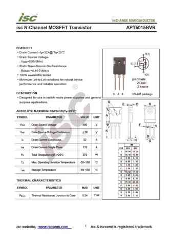
isc N-Channel MOSFET Transistor APT5015BVR FEATURES Drain Current I =32A@ T =25 D C Drain Source Voltage- V =500V(Min) DSS Static Drain-Source On-Resistance R =0.15 (Max) DS(on) 100% avalanche tested Minimum Lot-to-Lot variations for robust device performance and reliable operation DESCRIPTION Designed for use in switch mode power supplies and general purpo
apt5015bvfrg.pdf
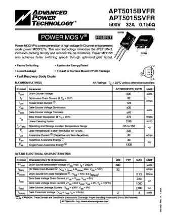
APT5015BVFR APT5015SVFR 500V 32A 0.150 BVFR POWER MOS V FREDFET D3PAK TO-247 Power MOS V is a new generation of high voltage N-Channel enhancement mode power MOSFETs. This new technology minimizes the JFET effect, increases packing density and reduces the on-resistance. Power MOS V SVFR also achieves faster switching speeds through optimized gate layout.
apt5015bvfr.pdf
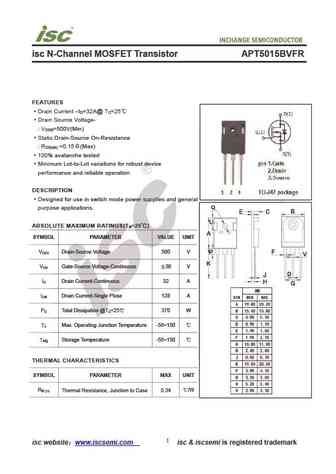
isc N-Channel MOSFET Transistor APT5015BVFR FEATURES Drain Current I =32A@ T =25 D C Drain Source Voltage- V =500V(Min) DSS Static Drain-Source On-Resistance R =0.15 (Max) DS(on) 100% avalanche tested Minimum Lot-to-Lot variations for robust device performance and reliable operation DESCRIPTION Designed for use in switch mode power supplies and general purp
Otros transistores... APT5010JN, APT5010JVFR, APT5010JVR, APT5010LVFR, APT5010LVR, APT5012WVR, APT5014B2VR, APT5014LVR, 13N50, APT5017BVFR, APT5017BVR, APT5017SVR, APT5019HVR, APT5020BN, APT5020BVFR, APT5020BVR, APT5020SVFR
History: SST4119
🌐 : EN ES РУ

Liste
Recientemente añadidas las descripciónes de los transistores:
MOSFET: AUW033N08BG | AUW025N10 | AUR030N10 | AUR020N10 | AUR020N085 | AUR014N10 | AUP074N10 | AUP065N10 | AUP062N08BG | AUP060N08AG | HYG053N10NS1B | HYG053N10NS1P | AP220N04T | AP220N04P | QM3126M3 | AUP060N055
Popular searches
tip36c transistor | 2sc3320 | 2sc2078 | ac127 transistor | a42 transistor | bc547c | 2sa726 | 2sd313