IPB031NE7N3G MOSFET Equivalente. Reemplazo. Hoja de especificaciones. Principales características
Número de Parte: IPB031NE7N3G
Tipo de FET: MOSFET
Polaridad de transistor: N
ESPECIFICACIONES MÁXIMAS
Pdⓘ - Máxima disipación de potencia: 214 W
|Vds|ⓘ - Voltaje máximo drenador-fuente: 75 V
|Vgs|ⓘ - Voltaje máximo fuente-puerta: 20 V
|Id|ⓘ - Corriente continua de drenaje: 100 A
Tjⓘ - Temperatura máxima de unión: 175 °C
CARACTERÍSTICAS ELÉCTRICAS
trⓘ - Tiempo de subida: 85 nS
Cossⓘ - Capacitancia de salida: 1380 pF
RDSonⓘ - Resistencia estado encendido drenaje a fuente: 0.0031 Ohm
Encapsulados: TO263
Búsqueda de reemplazo de IPB031NE7N3G MOSFET
- Selecciónⓘ de transistores por parámetros
IPB031NE7N3G datasheet
ipb031ne7n3 ipb031ne7n3g.pdf
IPB031NE7N3 G TM 3 Power-Transistor Product Summary Features V 7 D Q ( @D9=9J54 D538>??EC B53D96931D9?> R 1 m D n) m x Q #4513I CG9D389>7 1>4 3?>F5BD5BC I 1 D Q H35
ipb031ne7n3.pdf
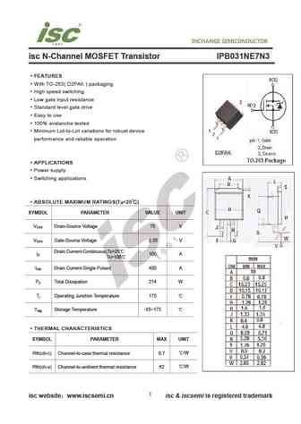
INCHANGE Semiconductor isc N-Channel MOSFET Transistor IPB031NE7N3 FEATURES With TO-263( D2PAK ) packaging High speed switching Low gate input resistance Standard level gate drive Easy to use 100% avalanche tested Minimum Lot-to-Lot variations for robust device performance and reliable operation APPLICATIONS Power supply Switching applications ABSOLUTE MAXI
ipb031n08n5.pdf
MOSFET Metal Oxide Semiconductor Field Effect Transistor OptiMOSTM OptiMOS 5 Power-Transistor, 80 V IPB031N08N5 Data Sheet Rev. 2.0 Final Power Management & Multimarket OptiMOS 5 Power-Transistor, 80 V IPB031N08N5 D PAK 1 Description Features Ideal for high frequency switching and sync. rec. Excellent gate charge x R product (FOM) DS(on) Very low on-resistance R
ipb031n08n5.pdf
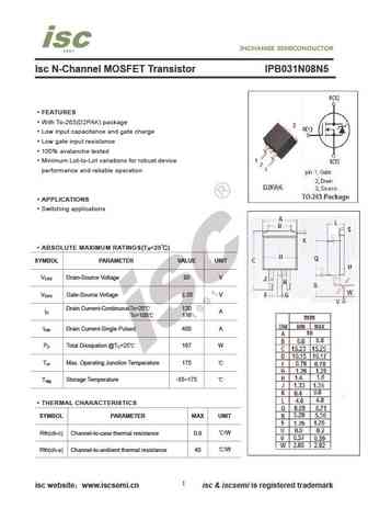
Isc N-Channel MOSFET Transistor IPB031N08N5 FEATURES With To-263(D2PAK) package Low input capacitance and gate charge Low gate input resistance 100% avalanche tested Minimum Lot-to-Lot variations for robust device performance and reliable operation APPLICATIONS Switching applications ABSOLUTE MAXIMUM RATINGS(T =25 ) a SYMBOL PARAMETER VALUE UNIT V Drain-Source V
Otros transistores... IPB022N04LG, IPB023N04NG, IPB023N06N3G, IPB025N08N3G, IPB025N10N3G, IPB027N10N3G, IPB029N06N3G, IPB030N08N3G, IRFP260N, IPB034N03LG, IPB034N06L3G, IPB034N06N3G, IPB035N08N3G, IPB036N12N3G, IPB037N06N3G, IPB038N12N3G, IPB039N04LG
🌐 : EN ES РУ

Liste
Recientemente añadidas las descripciónes de los transistores:
MOSFET: AUP060N055 | AUP056N10 | AUP056N08BGL | AUP052N085 | AUP045N12 | AUP039N10 | AUP034N10 | AUP034N06 | AUP033N08BG | AUP026N085 | AUN084N10 | AUN065N10 | AUN063N10 | AUN062N08BG | AUN060N08AG | AUN053N10
Popular searches
2sd1047 | 2n3035 | ksc1815 | bu406 | j201 datasheet | 2n5088 datasheet | irfp064n | tip31 transistor