IPB031NE7N3G Datasheet. Specs and Replacement
Type Designator: IPB031NE7N3G 📄📄
Type of Transistor: MOSFET
Type of Control Channel: N-Channel
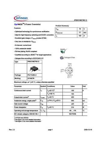
Absolute Maximum Ratings
Pd ⓘ - Maximum Power Dissipation: 214 W
|Vds|ⓘ - Maximum Drain-Source Voltage: 75 V
|Vgs|ⓘ - Maximum Gate-Source Voltage: 20 V
|Id| ⓘ - Maximum Drain Current: 100 A
Tj ⓘ - Maximum Junction Temperature: 175 °C
Electrical Characteristics
tr ⓘ - Rise Time: 85 nS
Cossⓘ - Output Capacitance: 1380 pF
RDSonⓘ - Maximum Drain-Source On-State Resistance: 0.0031 Ohm
Package: TO263
📄📄 Copy
IPB031NE7N3G substitution
- MOSFET ⓘ Cross-Reference Search
IPB031NE7N3G datasheet
ipb031ne7n3 ipb031ne7n3g.pdf
IPB031NE7N3 G TM 3 Power-Transistor Product Summary Features V 7 D Q ( @D9=9J54 D538>??EC B53D96931D9?> R 1 m D n) m x Q #4513I CG9D389>7 1>4 3?>F5BD5BC I 1 D Q H35... See More ⇒
ipb031ne7n3.pdf
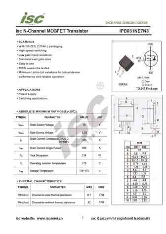
INCHANGE Semiconductor isc N-Channel MOSFET Transistor IPB031NE7N3 FEATURES With TO-263( D2PAK ) packaging High speed switching Low gate input resistance Standard level gate drive Easy to use 100% avalanche tested Minimum Lot-to-Lot variations for robust device performance and reliable operation APPLICATIONS Power supply Switching applications ABSOLUTE MAXI... See More ⇒
ipb031n08n5.pdf
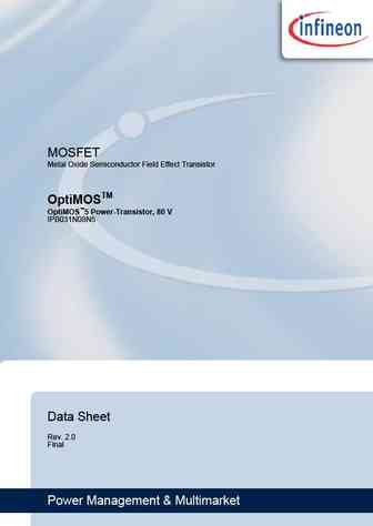
MOSFET Metal Oxide Semiconductor Field Effect Transistor OptiMOSTM OptiMOS 5 Power-Transistor, 80 V IPB031N08N5 Data Sheet Rev. 2.0 Final Power Management & Multimarket OptiMOS 5 Power-Transistor, 80 V IPB031N08N5 D PAK 1 Description Features Ideal for high frequency switching and sync. rec. Excellent gate charge x R product (FOM) DS(on) Very low on-resistance R... See More ⇒
ipb031n08n5.pdf
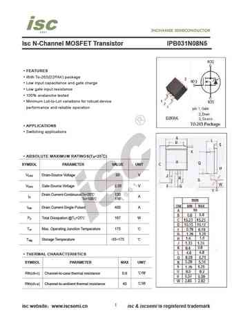
Isc N-Channel MOSFET Transistor IPB031N08N5 FEATURES With To-263(D2PAK) package Low input capacitance and gate charge Low gate input resistance 100% avalanche tested Minimum Lot-to-Lot variations for robust device performance and reliable operation APPLICATIONS Switching applications ABSOLUTE MAXIMUM RATINGS(T =25 ) a SYMBOL PARAMETER VALUE UNIT V Drain-Source V... See More ⇒
Detailed specifications: IPB022N04LG, IPB023N04NG, IPB023N06N3G, IPB025N08N3G, IPB025N10N3G, IPB027N10N3G, IPB029N06N3G, IPB030N08N3G, IRFZ44, IPB034N03LG, IPB034N06L3G, IPB034N06N3G, IPB035N08N3G, IPB036N12N3G, IPB037N06N3G, IPB038N12N3G, IPB039N04LG
Keywords - IPB031NE7N3G MOSFET specs
IPB031NE7N3G cross reference
IPB031NE7N3G equivalent finder
IPB031NE7N3G pdf lookup
IPB031NE7N3G substitution
IPB031NE7N3G replacement
Step-by-step guide to finding a MOSFET replacement. Cross-reference parts and ensure compatibility for your repair or project.
MOSFET Parameters. How They Affect Each Other
🌐 : EN ES РУ

LIST
Last Update
MOSFET: BC2301 | BC1012W | BC1012T | BC1012 | 2SK3019WT | 2SK3019W | 2SK3018WT | CS95118 | CS85105A | CS75N45
Popular searches
2sd1047 | 2n3035 | ksc1815 | bu406 | j201 datasheet | 2n5088 datasheet | irfp064n | tip31 transistor