IPP072N10N3G Datasheet. Equivalente. Reemplazo. Hoja de especificaciones. Principales características
Número de Parte: IPP072N10N3G 📄📄
Tipo de FET: MOSFET
Polaridad de transistor: N
ESPECIFICACIONES MÁXIMAS
Pdⓘ - Máxima disipación de potencia: 150 W
|Vds|ⓘ - Voltaje máximo drenador-fuente: 100 V
|Vgs|ⓘ - Voltaje máximo fuente-puerta: 20 V
|Id|ⓘ - Corriente continua de drenaje: 80 A
Tjⓘ - Temperatura máxima de unión: 175 °C
CARACTERÍSTICAS ELÉCTRICAS
trⓘ - Tiempo de subida: 37 nS
Cossⓘ - Capacitancia de salida: 646 pF
RDSonⓘ - Resistencia estado encendido drenaje a fuente: 0.0072 Ohm
Encapsulados: TO220
📄📄 Copiar
Búsqueda de reemplazo de IPP072N10N3G MOSFET
- Selecciónⓘ de transistores por parámetros
IPP072N10N3G datasheet
3.1. Size:316K infineon
ipp072n10n3-g ipi072n10n3-g.pdf 
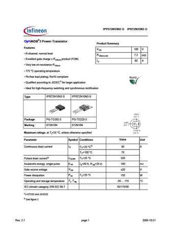
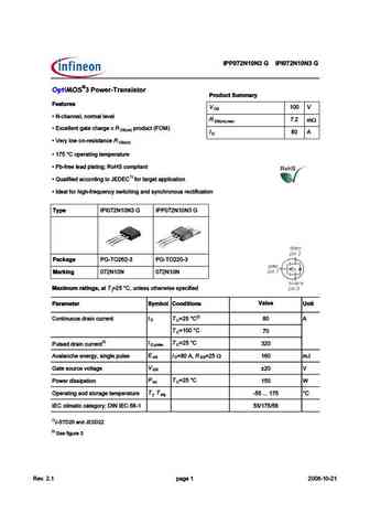
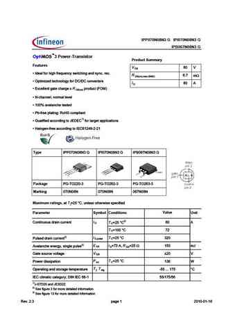
IPP072N10N3 G IPI072N10N3 G OptiMOS 3 Power-Transistor Product Summary Features V 100 V DS N-channel, normal level R 7.2 m DS(on),max Excellent gate charge x R product (FOM) DS(on) I 80 A D Very low on-resistance R DS(on) 175 C operating temperature Pb-free lead plating; RoHS compliant Qualified according to JEDEC1) for target application Id
3.2. Size:246K inchange semiconductor
ipp072n10n3.pdf
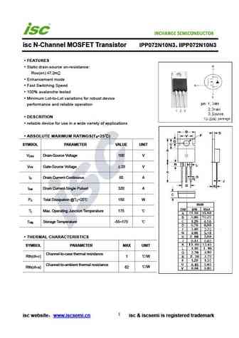
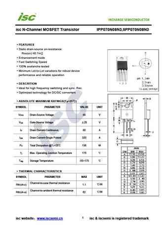
INCHANGE Semiconductor isc N-Channel MOSFET Transistor IPP072N10N3 IIPP072N10N3 FEATURES Static drain-source on-resistance RDS(on) 7.2m Enhancement mode Fast Switching Speed 100% avalanche tested Minimum Lot-to-Lot variations for robust device performance and reliable operation DESCRITION reliable device for use in a wide variety of applications ABSOLUTE
9.2. Size:1542K infineon
ipp076n15n5.pdf
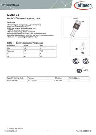
IPP076N15N5 MOSFET TO-220-3 OptiMOS 5 Power-Transistor, 150 V tab Features Excellent gate charge x R product (FOM) DS(on) Very low on-resistance R DS(on) Very low reverse recovery charge (Q rr) 175 C operating temperature Pb-free lead plating; RoHS compliant Qualified according to JEDEC1) for target application Ideal for high-frequency switching and
9.3. Size:162K infineon
ipp07n03l ipb07n03l.pdf
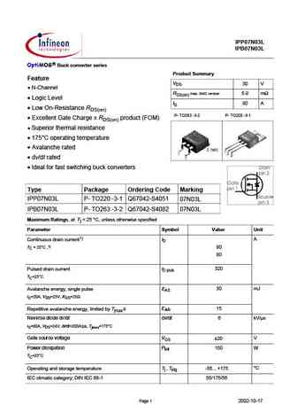
IPP07N03L IPB07N03L OptiMOS Buck converter series Product Summary Feature VDS 30 V N-Channel RDS(on) max. SMD version 5.9 m Logic Level ID 80 A Low On-Resistance RDS(on) P- TO263 -3-2 P- TO220 -3-1 Excellent Gate Charge x RDS(on) product (FOM) Superior thermal resistance 175 C operating temperature Avalanche rated dv/dt rated Ideal for f
9.4. Size:1021K infineon
ipp070n08n3 ipp070n08n3 ipi070n08n3 ipb067n08n3.pdf
IPP070N08N3 G IPI070N08N3 G IPB067N08N3 G 3 Power-Transistor Product Summary Features V D Q #4513I CG9D389>7 1>4 CI>3 B53 R 7 m , ?> =1H ,& Q ( @D9=9J54 D538>?F5BD5BC I D Q H35>5?B=1
9.5. Size:571K infineon
ipp076n12n3g ipi076n12n3g.pdf
$ " " $$ " " TM $;B1= '=- >5>?;= $=;0@/? &@99-=D Features 1 D R ( 492??6= ?@C>2= =6G6= 7 m D n)m x R I46==6?E 82E6 492C86 I AC@5F4E !) ' D n) 1 D R /6CJ =@H @? C6D DE2?46 D n) R U @A6C2E ?8 E6>A6C2EFC6 R *3 7C66 =625 A=2E ?8 , @#- 4@>A= 2?E 92=@86? 7C66 1) R + F2= 7 65 244@C5 ?8 E@ % 7@C E2C86E 2AA= 42E @? R $562= 7@C 9 89 7C6BF6?4J DH E49 ?8 2?5 DJ?49C@?@FD C64E
9.6. Size:545K infineon
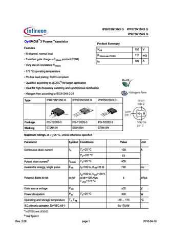
ipi076n12n3g ipp076n12n3g.pdf
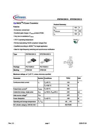
IPI076N12N3 G IPP076N12N3 G OptiMOSTM3 Power-Transistor Product Summary Features VDS 120 V N-channel, normal level RDS(on)max 7.6 mW Excellent gate charge x R product (FOM) DS(on) ID 100 A Very low on-resistance R DS(on) 175 C operating temperature Pb-free lead plating; RoHS compliant; halogen free Qualified according to JEDEC1) for target applicati
9.7. Size:1013K infineon
ipp070n08n3g ipi070n08n3g ipb067n08n3g.pdf

IPP070N08N3 G IPI070N08N3 G IPB067N08N3 G 3 Power-Transistor Product Summary Features V D Q #4513I CG9D389>7 1>4 CI>3 B53 R 7 m , ?> =1H ,& Q ( @D9=9J54 D538>?F5BD5BC I D Q H35>5?B=1
9.8. Size:894K infineon
ipb070n06ng ipp070n06ng ipi070n06ngrev1.4.pdf
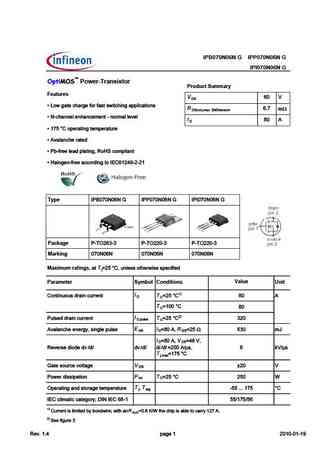
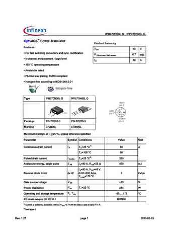
IPB070N06N G IPP070N06N G IPI070N06N G Power-Transistor Product Summary Features V D P &?F 71C5 381A75 6?A 61BC BF9C389>7 1@@B R 7 m , ?> =1G ,' E5AB9?> P ( 381>>581>35=5>C >?A=1
9.10. Size:424K infineon
ipb072n15n3-g ipp075n15n3-g ipi075n15n3-g.pdf
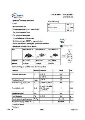
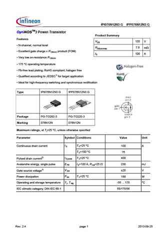
IPB072N15N3 G IPP075N15N3 G IPI075N15N3 G OptiMOS 3 Power-Transistor Product Summary Features V 150 V DS N-channel, normal level R 7.2 m DS(on),max (TO263) Excellent gate charge x R product (FOM) DS(on) I 100 A D Very low on-resistance R DS(on) 175 C operating temperature Pb-free lead plating; RoHS compliant Qualified according to JEDEC1) for tar
9.11. Size:244K inchange semiconductor
ipp075n15n3.pdf

isc N-Channel MOSFET Transistor IPP075N15N3 IIPP075N15N3 FEATURES Static drain-source on-resistance RDS(on) 7.5m Enhancement mode Fast Switching Speed 100% avalanche tested Minimum Lot-to-Lot variations for robust device performance and reliable operation DESCRITION Efficient and reliable device for use in a wide variety of applications ABSOLUTE MAXIMUM R
9.12. Size:245K inchange semiconductor
ipp076n15n5.pdf

isc N-Channel MOSFET Transistor IPP076N15N5 IIPP076N15N5 FEATURES Static drain-source on-resistance RDS(on) 7.6m Enhancement mode Fast Switching Speed 100% avalanche tested Minimum Lot-to-Lot variations for robust device performance and reliable operation DESCRITION Ideal for high-frequency switching and synchronous rectification ABSOLUTE MAXIMUM RATINGS(T
9.14. Size:245K inchange semiconductor
ipp076n12n3.pdf
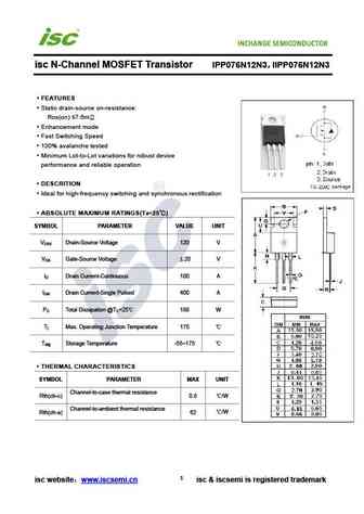
isc N-Channel MOSFET Transistor IPP076N12N3 IIPP076N12N3 FEATURES Static drain-source on-resistance RDS(on) 7.6m Enhancement mode Fast Switching Speed 100% avalanche tested Minimum Lot-to-Lot variations for robust device performance and reliable operation DESCRITION Ideal for high-frequency switching and synchronous rectification ABSOLUTE MAXIMUM RATINGS(
Otros transistores... IPP065N03LG, IPP065N04NG, IPP065N06LG, IPP06CN10LG, IPP06CN10NG, IPP070N06LG, IPP070N06NG, IPP070N08N3G, IRF730, IPP075N15N3G, IPP076N12N3G, IPP080N03LG, IPP080N06NG, IPP084N06L3G, IPP085N06LG, IPP086N10N3G, IPP08CN10LG