TK13A50DA MOSFET Equivalente. Reemplazo. Hoja de especificaciones. Principales características
Número de Parte: TK13A50DA
Tipo de FET: MOSFET
Polaridad de transistor: N
ESPECIFICACIONES MÁXIMAS
Pdⓘ - Máxima
disipación de potencia: 45 W
|Vds|ⓘ - Voltaje máximo drenador-fuente: 500 V
|Vgs|ⓘ - Voltaje máximo fuente-puerta: 30 V
|Id|ⓘ - Corriente continua
de drenaje: 12.5 A
Tjⓘ - Temperatura máxima de unión: 150 °C
CARACTERÍSTICAS ELÉCTRICAS
trⓘ - Tiempo
de subida: 25 nS
Cossⓘ - Capacitancia de salida: 165 pF
RDSonⓘ - Resistencia estado encendido drenaje a fuente: 0.47 Ohm
Encapsulados: TO220SIS
Búsqueda de reemplazo de TK13A50DA MOSFET
- Selecciónⓘ de transistores por parámetros
TK13A50DA datasheet
..1. Size:177K toshiba
tk13a50da.pdf 
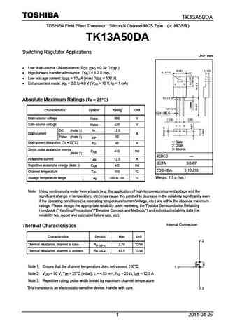
TK13A50DA TOSHIBA Field Effect Transistor Silicon N Channel MOS Type ( -MOS ) TK13A50DA Switching Regulator Applications Unit mm Low drain-source ON-resistance RDS (ON) = 0.39 (typ.) High forward transfer admittance Yfs = 6.0 S (typ.) Low leakage current IDSS = 10 A (max) (VDS = 500 V) Enhancement mode Vth = 2.0 to 4.0 V (VDS = 10 V, ID = 1 mA
..2. Size:253K inchange semiconductor
tk13a50da.pdf
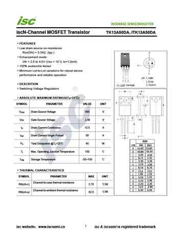
INCHANGE Semiconductor iscN-Channel MOSFET Transistor TK13A50DA ITK13A50DA FEATURES Low drain-source on-resistance RDS(ON) = 0.39 (typ.) Enhancement mode Vth = 2.0 to 4.0V (VDS = 10 V, ID=1.0mA) 100% avalanche tested Minimum Lot-to-Lot variations for robust device performance and reliable operation DESCRITION Switching Voltage Regulators ABSOLUTE MAXIMUM RAT
6.1. Size:184K toshiba
tk13a50d.pdf
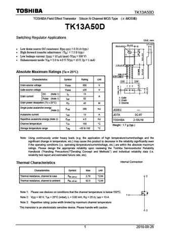
TK13A50D TOSHIBA Field Effect Transistor Silicon N Channel MOS Type ( -MOS ) TK13A50D Switching Regulator Applications Unit mm 2.7 0.2 10 0.3 3.2 0.2 A Low drain-source ON resistance RDS (ON) = 0.31 (typ.) High forward transfer admittance Yfs = 7.5 S (typ.) Low leakage current IDSS = 10 A (max) (VDS = 500 V) Enhancement-mode
8.1. Size:191K toshiba
tk13a55da.pdf

TK13A55DA TOSHIBA Field Effect Transistor Silicon N Channel MOS Type ( -MOS ) TK13A55DA Switching Regulator Applications Unit mm 2.7 0.2 10 0.3 3.2 0.2 A Low drain-source ON-resistance RDS (ON) = 0.32 (typ.) High forward transfer admittance Yfs = 6.0 S (typ.) Low leakage current IDSS = 10 A (max) (VDS = 550 V) Enhancement mode Vt
9.1. Size:228K toshiba
tk13a25d.pdf
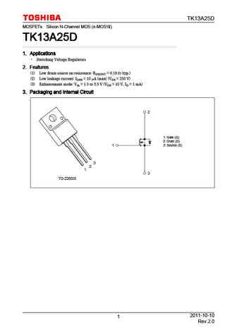
TK13A25D MOSFETs Silicon N-Channel MOS ( -MOS ) TK13A25D TK13A25D TK13A25D TK13A25D 1. Applications 1. Applications 1. Applications 1. Applications Switching Voltage Regulators 2. Features 2. Features 2. Features 2. Features (1) Low drain-source on-resistance RDS(ON) = 0.19 (typ.) (2) Low leakage current IDSS = 10 A (max) (VDS = 250 V) (3) Enhancement mode Vth =
9.2. Size:191K toshiba
tk13a60d.pdf
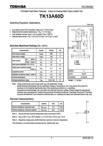
TK13A60D TOSHIBA Field Effect Transistor Silicon N Channel MOS Type ( -MOS VII) TK13A60D Switching Regulator Applications Unit mm Low drain-source ON-resistance RDS (ON) = 0.33 (typ.) High forward transfer admittance Yfs = 6.5 S (typ.) Low leakage current IDSS = 10 A (max) (VDS = 600 V) Enhancement mode Vth = 2.0 to 4.0 V (VDS = 10 V, ID = 1 mA) Ab
9.3. Size:226K toshiba
tk13a65d.pdf
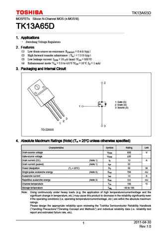
TK13A65D MOSFETs Silicon N-Channel MOS ( -MOS ) TK13A65D TK13A65D TK13A65D TK13A65D 1. Applications 1. Applications 1. Applications 1. Applications Switching Voltage Regulators 2. Features 2. Features 2. Features 2. Features (1) Low drain-source on-resistance RDS(ON) = 0.4 (typ.) (2) High forward transfer admittance Yfs = 7.5 S (typ.) (3) Low leakage current IDS
9.4. Size:213K toshiba
tk13a65u.pdf
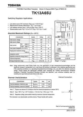
TK13A65U TOSHIBA Field Effect Transistor Silicon N Channel MOS Type (DTMOS II) TK13A65U Switching Regulator Applications Unit mm 2.7 0.2 10 0.3 3.2 0.2 A Low drain-source ON resistance RDS (ON) = 0.32 (typ.) High forward transfer admittance Yfs = 8.0 S (typ.) Low leakage current IDSS = 100 A (max) (VDS = 650 V) Enhancement-mod
9.5. Size:181K toshiba
tk13a45d.pdf
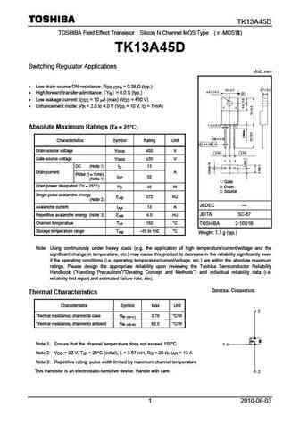
TK13A45D TOSHIBA Field Effect Transistor Silicon N Channel MOS Type ( -MOS ) TK13A45D Switching Regulator Applications Unit mm Low drain-source ON-resistance RDS (ON) = 0.38 (typ.) High forward transfer admittance Yfs = 6.0 S (typ.) Low leakage current IDSS = 10 A (max) (VDS = 450 V) Enhancement mode Vth = 2.0 to 4.0 V (VDS = 10 V, ID = 1 mA)
9.6. Size:252K inchange semiconductor
tk13a25d.pdf
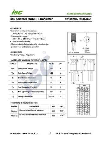
INCHANGE Semiconductor iscN-Channel MOSFET Transistor TK13A25D ITK13A25D FEATURES Low drain-source on-resistance RDS(ON) = 0.19 (typ.) (VGS = 10 V) Enhancement mode Vth = 1.5 to 3.5V (VDS = 10 V, ID=1.0mA) 100% avalanche tested Minimum Lot-to-Lot variations for robust device performance and reliable operation DESCRITION Switching Voltage Regulators ABSOLUTE MA
9.7. Size:252K inchange semiconductor
tk13a60d.pdf
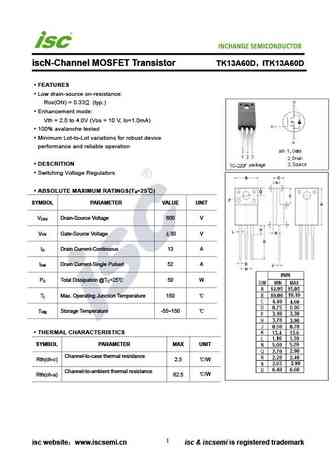
INCHANGE Semiconductor iscN-Channel MOSFET Transistor TK13A60D ITK13A60D FEATURES Low drain-source on-resistance RDS(ON) = 0.33 (typ.) Enhancement mode Vth = 2.0 to 4.0V (VDS = 10 V, ID=1.0mA) 100% avalanche tested Minimum Lot-to-Lot variations for robust device performance and reliable operation DESCRITION Switching Voltage Regulators ABSOLUTE MAXIMUM RATINGS
9.8. Size:255K inchange semiconductor
tk13a60w.pdf
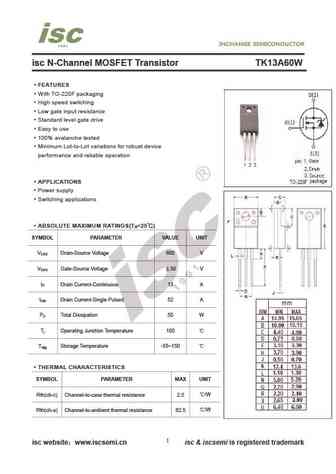
isc N-Channel MOSFET Transistor TK13A60W FEATURES With TO-220F packaging High speed switching Low gate input resistance Standard level gate drive Easy to use 100% avalanche tested Minimum Lot-to-Lot variations for robust device performance and reliable operation APPLICATIONS Power supply Switching applications ABSOLUTE MAXIMUM RATINGS(T =25 ) a SYMBOL PA
9.9. Size:257K inchange semiconductor
tk13a65d.pdf
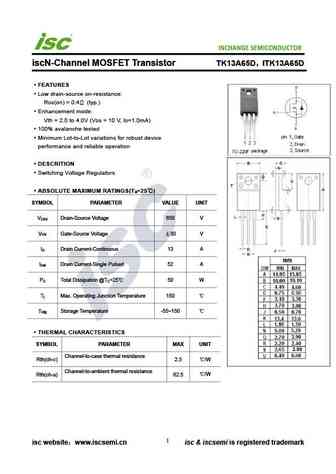
INCHANGE Semiconductor iscN-Channel MOSFET Transistor TK13A65D ITK13A65D FEATURES Low drain-source on-resistance RDS(on) = 0.4 (typ.) Enhancement mode Vth = 2.0 to 4.0V (VDS = 10 V, ID=1.0mA) 100% avalanche tested Minimum Lot-to-Lot variations for robust device performance and reliable operation DESCRITION Switching Voltage Regulators ABSOLUTE MAXIMUM RATINGS(
9.10. Size:253K inchange semiconductor
tk13a65u.pdf
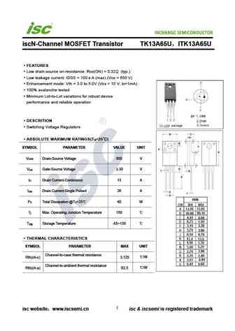
INCHANGE Semiconductor iscN-Channel MOSFET Transistor TK13A65U ITK13A65U FEATURES Low drain-source on-resistance RDS(ON) = 0.32 (typ.) Low leakage current IDSS = 100 A (max) (VDS = 650 V) Enhancement mode Vth = 3.0 to 5.0V (VDS = 10 V, ID=1mA) 100% avalanche tested Minimum Lot-to-Lot variations for robust device performance and reliable operation DESCRITION Sw
9.11. Size:253K inchange semiconductor
tk13a45d.pdf

INCHANGE Semiconductor iscN-Channel MOSFET Transistor TK13A45D ITK13A45D FEATURES Low drain-source on-resistance RDS(ON) = 0.38 (typ.) Enhancement mode Vth = 2.0 to 4.0V (VDS = 10 V, ID=1.0mA) 100% avalanche tested Minimum Lot-to-Lot variations for robust device performance and reliable operation DESCRITION Switching Voltage Regulators ABSOLUTE MAXIMUM RATINGS
Otros transistores... TK12E60U, TK12J55D, TK12J60U, TK12X53D, TK12X60U, TK130F06K3, TK13A25D, TK13A45D, IRF540, TK13A50D, TK13A55DA, TK13A60D, TK13A65D, TK13A65U, TK13E25D, TK13J65U, TK13P25D
