TK20J50D MOSFET Equivalente. Reemplazo. Hoja de especificaciones. Principales características
Número de Parte: TK20J50D
Tipo de FET: MOSFET
Polaridad de transistor: N
ESPECIFICACIONES MÁXIMAS
Pdⓘ - Máxima disipación de potencia: 280 W
|Vds|ⓘ - Voltaje máximo drenador-fuente: 500 V
|Vgs|ⓘ - Voltaje máximo fuente-puerta: 30 V
|Id|ⓘ - Corriente continua de drenaje: 20 A
Tjⓘ - Temperatura máxima de unión: 150 °C
CARACTERÍSTICAS ELÉCTRICAS
trⓘ - Tiempo de subida: 50 nS
Cossⓘ - Capacitancia de salida: 280 pF
RDSonⓘ - Resistencia estado encendido drenaje a fuente: 0.27 Ohm
Búsqueda de reemplazo de TK20J50D MOSFET
- Selecciónⓘ de transistores por parámetros
TK20J50D datasheet
tk20j50d.pdf
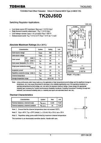
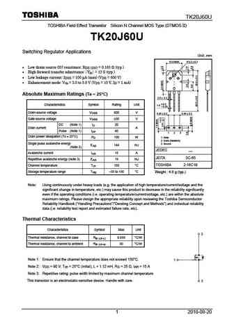
TK20J50D TOSHIBA Field Effect Transistor Silicon N Channel MOS Type ( -MOS VII) TK20J50D Switching Regulator Applications Unit mm 15.9 MAX. 3.2 0.2 Low drain-source ON-resistance RDS (ON) = 0.22 (typ.) High forward transfer admittance Yfs = 8.5 S (typ.) Low leakage current IDSS = 10 A (max) (VDS = 500 V) Enhancement mode Vth = 2.0 to 4.0 V (V
tk20j50d.pdf
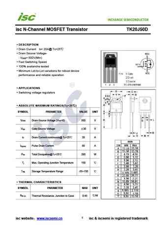
isc N-Channel MOSFET Transistor TK20J50D DESCRIPTION Drain Current I = 20A@ T =25 D C Drain Source Voltage- V = 500V(Min) DSS Fast Switching Speed 100% avalanche tested Minimum Lot-to-Lot variations for robust device performance and reliable operation APPLICATIONS Switching voltage regulators ABSOLUTE MAXIMUM RATINGS(T =25 ) C SYMBOL PARAMETER VALUE UNIT
tk20j60w5.pdf
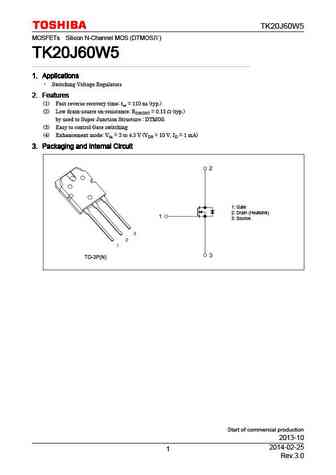
TK20J60W5 MOSFETs Silicon N-Channel MOS (DTMOS ) TK20J60W5 TK20J60W5 TK20J60W5 TK20J60W5 1. Applications 1. Applications 1. Applications 1. Applications Switching Voltage Regulators 2. Features 2. Features 2. Features 2. Features (1) Fast reverse recovery time trr = 110 ns (typ.) (2) Low drain-source on-resistance RDS(ON) = 0.15 (typ.) by used to Super Junction Str
tk20j60w.pdf

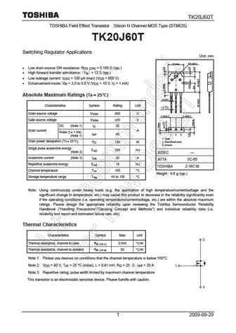
TK20J60W MOSFETs Silicon N-Channel MOS (DTMOS ) TK20J60W TK20J60W TK20J60W TK20J60W 1. Applications 1. Applications 1. Applications 1. Applications Switching Voltage Regulators 2. Features 2. Features 2. Features 2. Features (1) Low drain-source on-resistance RDS(ON) = 0.13 (typ.) by used to Super Junction Structure DTMOS (2) Easy to control Gate switching (3) En
Otros transistores... TK18A60V, TK19A45D, TK19J55D, TK1P90A, TK1Q90A, TK20A25D, TK20A60U, TK20E60U, K4145, TK20J60U, TK20P04M1, TK20S04K3L, TK20S06K3L, TK20X60U, TK25A10K3, TK25A20D, TK2A65D
🌐 : EN ES РУ

Liste
Recientemente añadidas las descripciónes de los transistores:
MOSFET: AKF30N5P0SX | AKF30N10S | AKF20P45D | CM4407 | CM3407 | CM3400 | SVF11N65F | SVF11N65T | FKBB3105 | EHBA036R1 | CRTT067N10N | AP6NA3R2MT | AP65SA145DDT8 | AP4NAR95CMT-A | AP4024GEMT-HF | AP3P050AH
Popular searches
2sd1047 transistor | mj802 | bu508a | bc560c | ksa1220ay | irf 830 | mpsa56 transistor | transistor 2222a