FDC6304P MOSFET Equivalente. Reemplazo. Hoja de especificaciones. Principales características
Número de Parte: FDC6304P
Tipo de FET: MOSFET
Polaridad de transistor: P
ESPECIFICACIONES MÁXIMAS
Pdⓘ - Máxima disipación de potencia: 0.9 W
|Vds|ⓘ - Voltaje máximo drenador-fuente: 25 V
|Vgs|ⓘ - Voltaje máximo fuente-puerta: 8 V
|Id|ⓘ - Corriente continua de drenaje: 0.46 A
Tjⓘ - Temperatura máxima de unión: 150 °C
CARACTERÍSTICAS ELÉCTRICAS
trⓘ - Tiempo de subida: 8 nS
Cossⓘ - Capacitancia de salida: 35 pF
RDSonⓘ - Resistencia estado encendido drenaje a fuente: 1.1 Ohm
Encapsulados: SUPERSOT6
Búsqueda de reemplazo de FDC6304P MOSFET
- Selecciónⓘ de transistores por parámetros
FDC6304P datasheet
fdc6304p.pdf
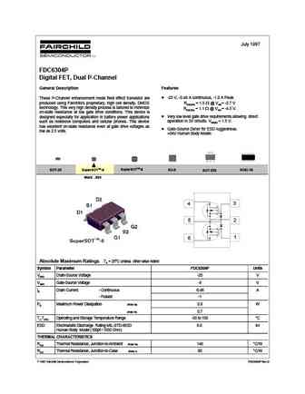
July 1997 FDC6304P Digital FET, Dual P-Channel General Description Features -25 V, -0.46 A continuous, -1.0 A Peak. These P-Channel enhancement mode field effect transistor are produced using Fairchild's proprietary, high cell density, DMOS RDS(ON) = 1.5 @ VGS= -2.7 V technology. This very high density process is tailored to minimize RDS(ON) = 1.1 @ VGS = -4.5 V. on-state
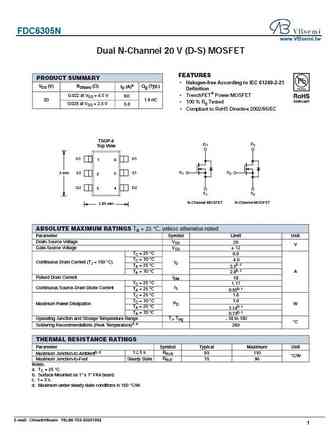
fdc6305n.pdf
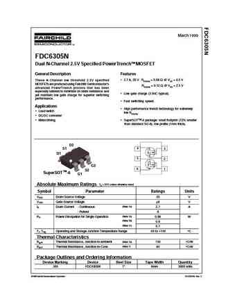
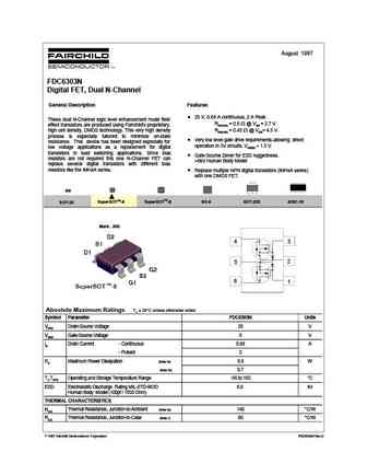
March 1999 FDC6305N Dual N-Channel 2.5V Specified PowerTrenchTM MOSFET General Description Features 2.7 A, 20 V. RDS(ON) = 0.08 @ VGS = 4.5 V These N-Channel low threshold 2.5V specified MOSFETs are produced using Fairchild Semiconductor's RDS(ON) = 0.12 @ VGS = 2.5 V advanced PowerTrench process that has been especially tailored to minimize on-state resistance and Low
fdc6306p.pdf
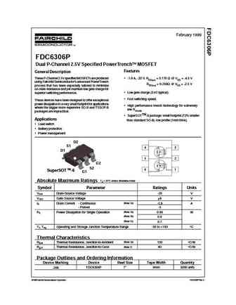
February 1999 FDC6306P Dual P-Channel 2.5V Specified PowerTrench MOSFET Features General Description These P-Channel 2.5V specified MOSFETs are produced -1.9 A, -20 V. RDS(on) = 0.170 @ VGS = -4.5 V using Fairchild Semiconductor's advanced PowerTrench RDS(on) = 0.250 @ VGS = -2.5 V process that has been especially tailored to minimize on-state resistance and yet maintain
fdc6302p.pdf
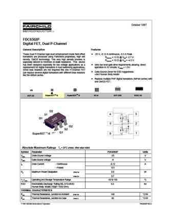
October 1997 FDC6302P Digital FET, Dual P-Channel General Description Features These Dual P-Channel logic level enhancement mode field effect -25 V, -0.12 A continuous, -0.5 A Peak. transistors are produced using Fairchild's proprietary, high cell RDS(ON) = 13 @ VGS= -2.7 V density, DMOS technology. This very high density process is RDS(ON) = 10 @ VGS = -4.5 V. especially


Otros transistores... FDB7030L, FDB7045L, FDB8030L, AS3401, FDC5612, FDC6301N, FDC6302P, FDC6303N, AON6380, FDC6305N, FDC6306P, FDC6308P, FDC633N, FDC634P, FDC636P, FDC637AN, FDC638P
🌐 : EN ES РУ

Liste
Recientemente añadidas las descripciónes de los transistores:
MOSFET: AUP060N055 | AUP056N10 | AUP056N08BGL | AUP052N085 | AUP045N12 | AUP039N10 | AUP034N10 | AUP034N06 | AUP033N08BG | AUP026N085 | AUN084N10 | AUN065N10 | AUN063N10 | AUN062N08BG | AUN060N08AG | AUN053N10
Popular searches
2sa1106 | 2sb56 | 2sc1451 datasheet | 2sc373 | a1023 datasheet | 2sc1080 | 2sb618 | 2sc1328