CES2312 Datasheet. Equivalente. Reemplazo. Hoja de especificaciones. Principales características
Número de Parte: CES2312 📄📄
Tipo de FET: MOSFET
Polaridad de transistor: N
ESPECIFICACIONES MÁXIMAS
Pdⓘ - Máxima disipación de potencia: 1.3 W
|Vds|ⓘ - Voltaje máximo drenador-fuente: 20 V
|Vgs|ⓘ - Voltaje máximo fuente-puerta: 8 V
|Id|ⓘ - Corriente continua de drenaje: 4.5 A
Tjⓘ - Temperatura máxima de unión: 150 °C
CARACTERÍSTICAS ELÉCTRICAS
trⓘ - Tiempo de subida: 18 nS
Cossⓘ - Capacitancia de salida: 300 pF
RDSonⓘ - Resistencia estado encendido drenaje a fuente: 0.033 Ohm
Encapsulados: SOT23
📄📄 Copiar
Búsqueda de reemplazo de CES2312 MOSFET
- Selecciónⓘ de transistores por parámetros
CES2312 datasheet
ces2312.pdf
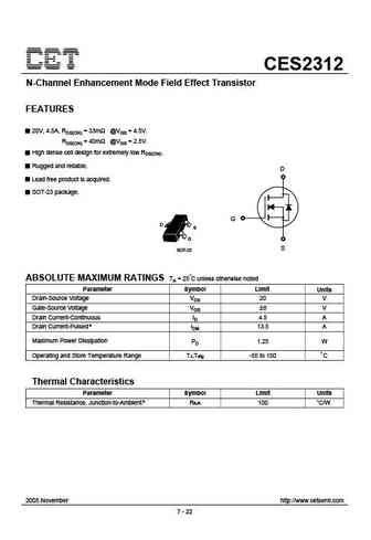
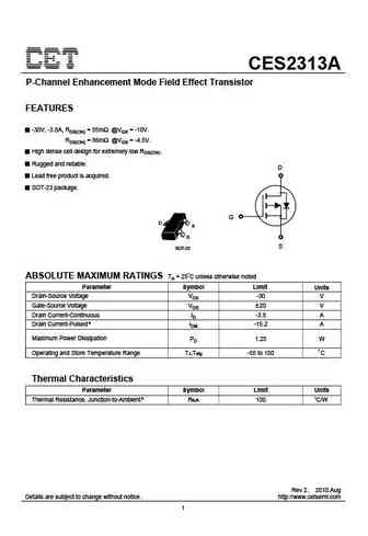
CES2312 N-Channel Enhancement Mode Field Effect Transistor FEATURES 20V, 4.5A, RDS(ON) = 33m @VGS = 4.5V. RDS(ON) = 40m @VGS = 2.5V. High dense cell design for extremely low RDS(ON). Rugged and reliable. D Lead free product is acquired. SOT-23 package. G D S G S SOT-23 ABSOLUTE MAXIMUM RATINGS TA = 25 C unless otherwise noted Parameter Symbol Limit Units Drain-Source Vo
ces2317.pdf

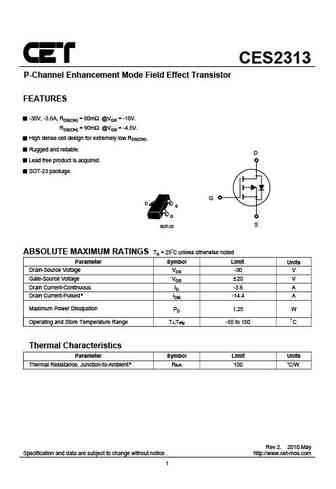
CES2317 P-Channel Enhancement Mode Field Effect Transistor FEATURES -30V, -3.1A, RDS(ON) = 80m @VGS = -10V. RDS(ON) = 90m @VGS = -4.5V. RDS(ON) = 120m @VGS = -2.5V. High dense cell design for extremely low RDS(ON). D Rugged and reliable. Lead-free plating ; RoHS compliant. SOT-23 package. G D S G S SOT-23 ABSOLUTE MAXIMUM RATINGS TA = 25 C unless otherwise noted Par
ces2316.pdf
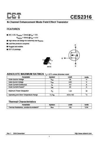
CES2316 N-Channel Enhancement Mode Field Effect Transistor FEATURES 30V, 4.8A, RDS(ON) = 34m @VGS = 10V. RDS(ON) = 50m @VGS = 4.5V. High dense cell design for extremely low RDS(ON). Lead free product is acquired. D Rugged and reliable. SOT-23 package. G D S G S SOT-23 ABSOLUTE MAXIMUM RATINGS TA = 25 C unless otherwise noted Parameter Symbol Limit Units Drain-Source Vol
ces2310.pdf
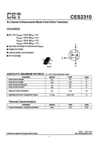
CES2310 N-Channel Enhancement Mode Field Effect Transistor FEATURES 30V, 4.8A, RDS(ON) = 34m @VGS = 10V. RDS(ON) = 38m @VGS = 4.5V. RDS(ON) = 50m @VGS = 2.5V. RDS(ON) = 60m @VGS = 1.8V. D High dense cell design for extremely low RDS(ON). Rugged and reliable. Lead-free plating ; RoHS compliant. SOT-23 package. G D S G S SOT-23 ABSOLUTE MAXIMUM RATINGS TA = 25 C u

Otros transistores... CEM9926A, CEM9935A, CEM9936A, CEN7002A, CES2302, CES2306, CES2308, CES2310, 50N06, CES2314, CES2316, CES2320, CES2324, CES2342, CES2362, CET0215, CET04N10
Parámetros del MOSFET. Cómo se afectan entre sí.
History: APT7F100B | APT8024JLL
🌐 : EN ES РУ

Liste
Recientemente añadidas las descripciónes de los transistores:
MOSFET: CS95118 | CS85105A | CS75N45 | CS72N12 | CS55N50 | CS48N75A | CS40N27 | MSQ60P04D | MSQ40P07D | MSQ30P40D | MSQ30P15 | MSQ30P07D | MSQ100N03D | MSHM60P14 | MSHM40N085 | MSHM30N46
Popular searches
30j127 datasheet | 2sc1116a | 2sc460 | 2sc869 datasheet | k3568 datasheet | 2sb77 | ac128 transistor datasheet | c2878 transistor