2SJ364 Datasheet. Equivalente. Reemplazo. Hoja de especificaciones. Principales características
Número de Parte: 2SJ364 📄📄
Tipo de FET: JFET
Polaridad de transistor: P
ESPECIFICACIONES MÁXIMAS
Pdⓘ - Máxima disipación de potencia: 0.15 W
|Vgs|ⓘ - Voltaje máximo fuente-puerta: 3.5 V
|Id|ⓘ - Corriente continua de drenaje: 0.02 A
Tjⓘ - Temperatura máxima de unión: 150 °C
CARACTERÍSTICAS ELÉCTRICAS
RDSonⓘ - Resistencia estado encendido drenaje a fuente: 300 Ohm
Encapsulados: SC70
📄📄 Copiar
Búsqueda de reemplazo de 2SJ364 MOSFET
- Selecciónⓘ de transistores por parámetros
2SJ364 datasheet
2sj364.pdf
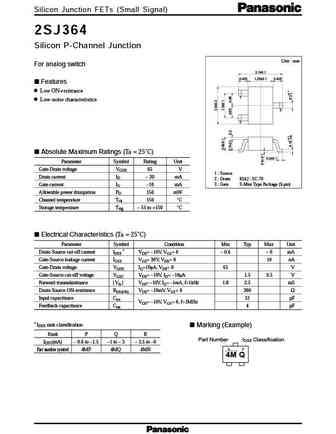
Silicon Junction FETs (Small Signal) 2SJ364 2SJ364 Silicon P-Channel Junction Unit mm For analog switch 2.1 0.1 0.425 1.25 0.1 0.425 Features Low ON-resistance 1 Low-noise characteristics 3 2 Absolute Maximum Ratings (Ta = 25 C) 0.2 0.1 Parameter Symbol Rating Unit Gate-Drain voltage VGDS 65 V 1 Source Drain current ID 20 mA 2 Drain EIAJ SC-70 Gate cur
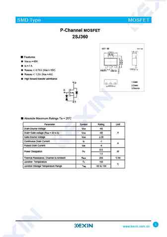
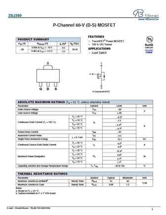
2sj360.pdf
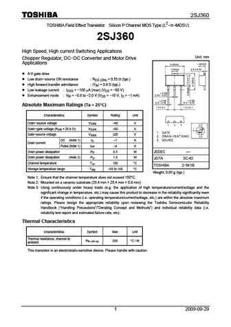
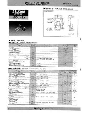
2SJ360 2 TOSHIBA Field Effect Transistor Silicon P Channel MOS Type (L - -MOSV) 2SJ360 High Speed, High current Switching Applications Unit mm Chopper Regulator, DC-DC Converter and Motor Drive Applications 4-V gate drive Low drain-source ON resistance RDS (ON) = 0.55 (typ.) High forward transfer admittance Yfs = 0.9 S (typ.) Low leakage current IDSS =
2sj362.pdf
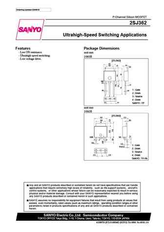
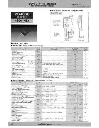
Ordering number EN4918 P-Channel Silicon MOSFET 2SJ362 Ultrahigh-Speed Switching Applications Features Package Dimensions Low ON resistance. unit mm Ultrahigh-speed switching. 2083B Low-voltage drive. [2SJ362] 6.5 2.3 5.0 0.5 4 0.85 0.7 1.2 1 Gate 0.6 0.5 2 Drain 1 2 3 3 Source 4 Drain 2.3 2.3 SANYO TP unit mm 2092B [2SJ362] 6.5 2.3 5.0 0.5
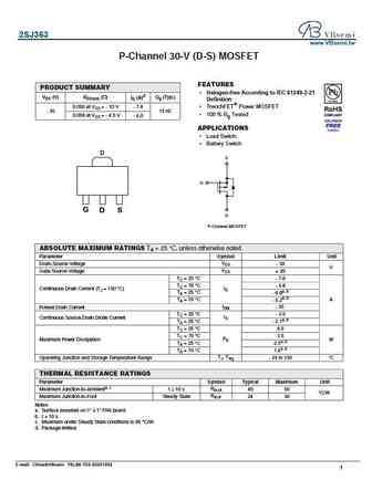
2sj363.pdf
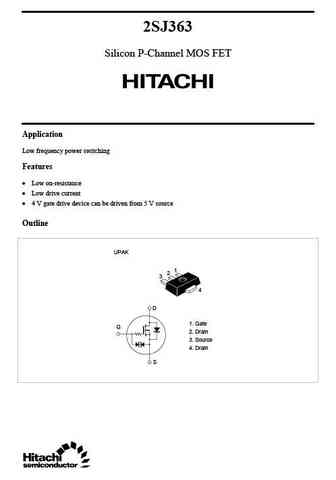
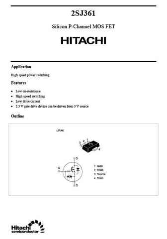
2SJ363 Silicon P-Channel MOS FET Application Low frequency power switching Features Low on-resistance Low drive current 4 V gate drive device can be driven from 5 V source Outline UPAK 1 2 3 4 D 1. Gate G 2. Drain 3. Source 4. Drain S 2SJ363 Absolute Maximum Ratings (Ta = 25 C) Item Symbol Ratings Unit Drain to source voltage VDSS 30 V Gate to source vo
Otros transistores... 2SJ181, 2SJ244, 2SJ307, 2SJ317, 2SJ319, 2SJ361, 2SJ362, 2SJ363, AON7506, 2SJ365, 2SJ368, 2SJ387, 2SJ399, 2SJ451, 2SJ48, 2SJ49, 2SJ50
🌐 : EN ES РУ

Liste
Recientemente añadidas las descripciónes de los transistores:
MOSFET: CS65N25AKR | AOL1718 | BCD70N07A | BCD90N03 | BCD80N06 | T50N06 | H50N06 | BCD12N65 | BCT12N65 | BCD4N65 | BCT4N65 | BCD7N65 | BCT7N65 | BCT20N65 | ASDM30P100KQ | ASDM30N90Q
Popular searches
irf630 datasheet | mpsa13 equivalent | c5198 | 2sc1969 transistor | bcy21 | s8550 datasheet | mj50ac100 | 2sc1318 replacement