J305 Datasheet. Equivalente. Reemplazo. Hoja de especificaciones. Principales características
Número de Parte: J305 📄📄
Tipo de FET: JFET
Polaridad de transistor: N
ESPECIFICACIONES MÁXIMAS
Pdⓘ - Máxima disipación de potencia: 0.35 W
|Vds|ⓘ - Voltaje máximo drenador-fuente: 30 V
|Vgs|ⓘ - Voltaje máximo fuente-puerta: 3 V
|Id|ⓘ - Corriente continua de drenaje: 0.008 A
Tjⓘ - Temperatura máxima de unión: 150 °C
CARACTERÍSTICAS ELÉCTRICAS
Encapsulados: TO-92
📄📄 Copiar
Búsqueda de reemplazo de J305 MOSFET
- Selecciónⓘ de transistores por parámetros
J305 datasheet
j305.pdf
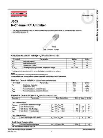
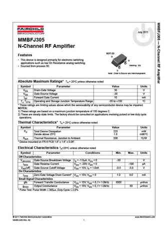
September 2007 J305 N-Channel RF Amplifier This device is designed primarily for electronic switching applications such as low on resistance analog switching. Sourced from process 50. TO-92 1 1. Gate 2. Source 3. Drain Absolute Maximum Ratings* Ta=25 C unless otherwise noted Symbol Parameter Value Units VDG Drain-Gate Voltage 30 V VGS Gate-Source Voltage -30 V IGF Forward G
j304 j305.pdf
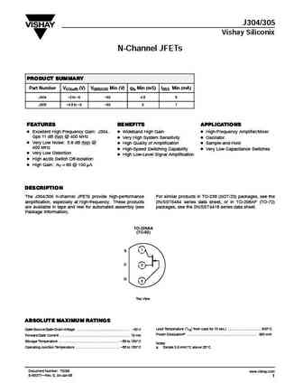
J304/305 Vishay Siliconix N-Channel JFETs PRODUCT SUMMARY Part Number VGS(off) (V) V(BR)GSS Min (V) gfs Min (mS) IDSS Min (mA) J304 -2 to -6 -30 4.5 5 J305 -0.5 to -3 -30 3 1 FEATURES BENEFITS APPLICATIONS D Excellent High Frequency Gain J304, D Wideband High Gain D High-Frequency Amplifier/Mixer Gps 11 dB (typ) @ 400 MHz D Very High System Sensitivity D Oscillator D Very Low Noise
2sj305.pdf
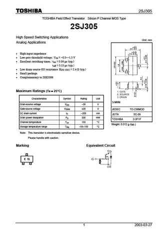
2SJ305 TOSHIBA Field Effect Transistor Silicon P Channel MOS Type 2SJ305 High Speed Switching Applications Unit mm Analog Applications High input impedance Low gate threshold voltage. V = -0.5 -1.5 V th Excellent switching times. t = 0.06 s (typ.) on t = 0.15 s (typ.) off Low drain-source ON resistance R = 2.4 (typ.) DS (ON) Small packa
ssm3j305t.pdf
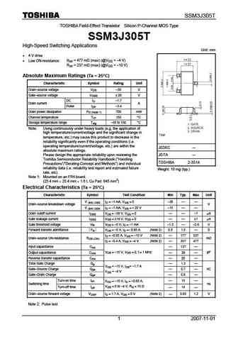
SSM3J305T TOSHIBA Field-Effect Transistor Silicon P-Channel MOS Type SSM3J305T High-Speed Switching Applications Unit mm 4 V drive Low ON-resistance Ron = 477 m (max) (@VGS = -4 V) Ron = 237 m (max) (@VGS = -10 V) Absolute Maximum Ratings (Ta = 25 C) Characteristic Symbol Rating Unit Drain source voltage VDS -30 V Gate source voltage VGSS 20 V DC ID
Otros transistores... MMBFJ202, J210, MMBFJ210, MMBFJ211, MMBFJ212, J270, J271, J304, 2N7002, KSK30, KSK595H, KSK596, LS4117, LS4118, LS4119, MMBF4091, MMBF4092
Parámetros del MOSFET. Cómo se afectan entre sí.
History: SI7415DN | 2SK795 | FDD7N20TM | P1604ETF | HM80N04 | NDB6050 | APT7F120B
🌐 : EN ES РУ

Liste
Recientemente añadidas las descripciónes de los transistores:
MOSFET: CS95118 | CS85105A | CS75N45 | CS72N12 | CS55N50 | CS48N75A | CS40N27 | MSQ60P04D | MSQ40P07D | MSQ30P40D | MSQ30P15 | MSQ30P07D | MSQ100N03D | MSHM60P14 | MSHM40N085 | MSHM30N46
Popular searches
2n3904 | bc547 datasheet | k3797 mosfet | bs170 datasheet | tip41c | irfp460 | irfz44n mosfet | lm317t datasheet