J305 Specs and Replacement
Type Designator: J305
Type of Transistor: JFET
Type of Control Channel: N-Channel
Absolute Maximum Ratings
Pd ⓘ - Maximum Power Dissipation: 0.35 W
|Vds|ⓘ - Maximum Drain-Source Voltage: 30 V
|Vgs|ⓘ - Maximum Gate-Source Voltage: 3 V
|Id| ⓘ - Maximum Drain Current: 0.008 A
Tj ⓘ - Maximum Junction Temperature: 150 °C
Electrical Characteristics
Package: TO-92
J305 substitution
- MOSFET ⓘ Cross-Reference Search
J305 datasheet
j305.pdf
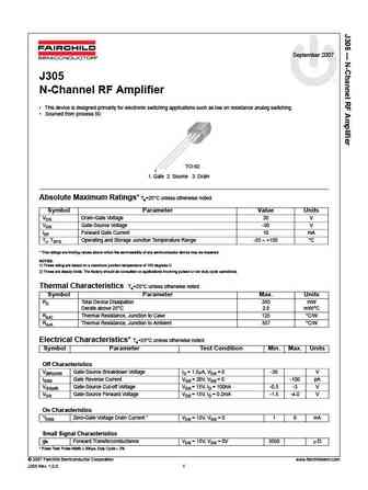
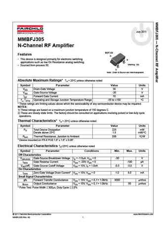
September 2007 J305 N-Channel RF Amplifier This device is designed primarily for electronic switching applications such as low on resistance analog switching. Sourced from process 50. TO-92 1 1. Gate 2. Source 3. Drain Absolute Maximum Ratings* Ta=25 C unless otherwise noted Symbol Parameter Value Units VDG Drain-Gate Voltage 30 V VGS Gate-Source Voltage -30 V IGF Forward G... See More ⇒
j304 j305.pdf
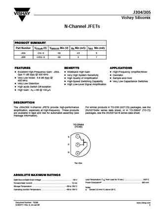
J304/305 Vishay Siliconix N-Channel JFETs PRODUCT SUMMARY Part Number VGS(off) (V) V(BR)GSS Min (V) gfs Min (mS) IDSS Min (mA) J304 -2 to -6 -30 4.5 5 J305 -0.5 to -3 -30 3 1 FEATURES BENEFITS APPLICATIONS D Excellent High Frequency Gain J304, D Wideband High Gain D High-Frequency Amplifier/Mixer Gps 11 dB (typ) @ 400 MHz D Very High System Sensitivity D Oscillator D Very Low Noise ... See More ⇒
2sj305.pdf
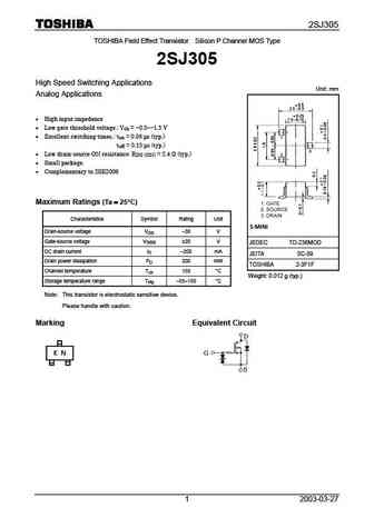
2SJ305 TOSHIBA Field Effect Transistor Silicon P Channel MOS Type 2SJ305 High Speed Switching Applications Unit mm Analog Applications High input impedance Low gate threshold voltage. V = -0.5 -1.5 V th Excellent switching times. t = 0.06 s (typ.) on t = 0.15 s (typ.) off Low drain-source ON resistance R = 2.4 (typ.) DS (ON) Small packa... See More ⇒
ssm3j305t.pdf
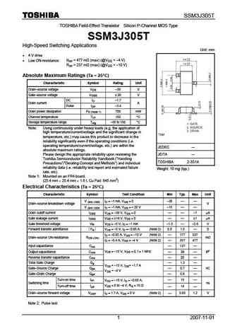
SSM3J305T TOSHIBA Field-Effect Transistor Silicon P-Channel MOS Type SSM3J305T High-Speed Switching Applications Unit mm 4 V drive Low ON-resistance Ron = 477 m (max) (@VGS = -4 V) Ron = 237 m (max) (@VGS = -10 V) Absolute Maximum Ratings (Ta = 25 C) Characteristic Symbol Rating Unit Drain source voltage VDS -30 V Gate source voltage VGSS 20 V DC ID ... See More ⇒
Detailed specifications: MMBFJ202 , J210 , MMBFJ210 , MMBFJ211 , MMBFJ212 , J270 , J271 , J304 , IRFB4110 , KSK30 , KSK595H , KSK596 , LS4117 , LS4118 , LS4119 , MMBF4091 , MMBF4092 .
Keywords - J305 MOSFET specs
J305 cross reference
J305 equivalent finder
J305 pdf lookup
J305 substitution
J305 replacement
Need a MOSFET replacement? Our guide shows you how to find a perfect substitute by comparing key parameters and specs
🌐 : EN ES РУ

LIST
Last Update
MOSFET: HAF1008S | HAF1008L | EMZB08P03H | CS30N20FA9R | AOT66613L | AOSP21313C | AOSP21311C | AOB66918L | AO3415C | AOTF20N40L
Popular searches
2n3904 | bc547 datasheet | k3797 mosfet | bs170 datasheet | tip41c | irfp460 | irfz44n mosfet | lm317t datasheet