MMBF5103 Datasheet. Equivalente. Reemplazo. Hoja de especificaciones. Principales características
Número de Parte: MMBF5103 📄📄
Tipo de FET: JFET
Polaridad de transistor: N
ESPECIFICACIONES MÁXIMAS
Pdⓘ - Máxima disipación de potencia: 0.35 W
|Vds|ⓘ - Voltaje máximo drenador-fuente: 40 V
|Vgs|ⓘ - Voltaje máximo fuente-puerta: 2.7 V
|Id|ⓘ - Corriente continua de drenaje: 0.04 A
Tjⓘ - Temperatura máxima de unión: 150 °C
CARACTERÍSTICAS ELÉCTRICAS
Encapsulados: SOT-23
📄📄 Copiar
Búsqueda de reemplazo de MMBF5103 MOSFET
- Selecciónⓘ de transistores por parámetros
MMBF5103 datasheet
mmbf5103.pdf
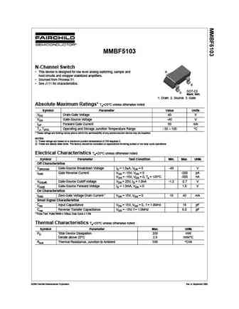
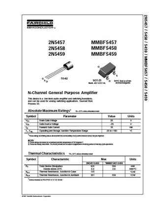
MMBF5103 N-Channel Switch G This device is designed for low level analog switching, sample and hold circuits and chopper stabilized amplifiers. Sourced from Process 51. See J111 for characteristics. S SOT-23 D Mark 66A 1. Drain 2. Source 3. Gate Absolute Maximum Ratings* Ta=25 C unless otherwise noted Symbol Parameter Value Units VDG Drain-Gate Voltage 40 V VGS Ga
mmbf5484lt1rev0d.pdf
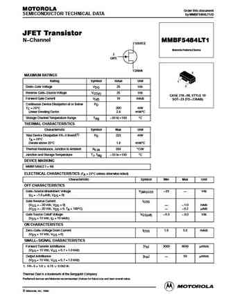
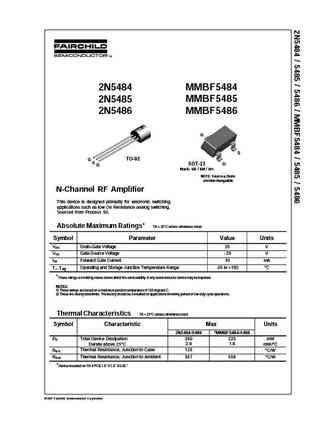
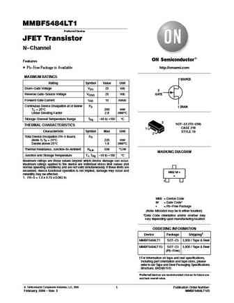
MOTOROLA Order this document SEMICONDUCTOR TECHNICAL DATA by MMBF5484LT1/D JFET Transistor N Channel MMBF5484LT1 2 SOURCE Motorola Preferred Device 3 GATE 1 DRAIN 3 MAXIMUM RATINGS Rating Symbol Value Unit 1 2 Drain Gate Voltage VDG 25 Vdc Reverse Gate Source Voltage VGS(r) 25 Vdc CASE 318 08, STYLE 10 Forward Gate Current IG(f) 10 mAdc SOT 23 (TO 236AB) Contin
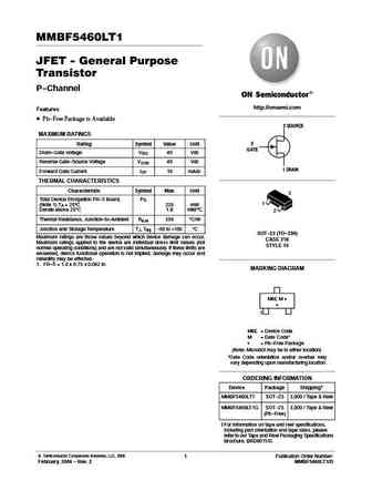
mmbf5457lt1rev0d.pdf
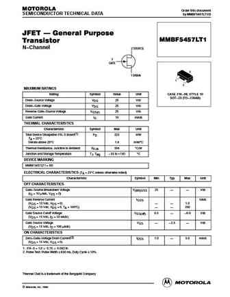
MOTOROLA Order this document SEMICONDUCTOR TECHNICAL DATA by MMBF5457LT1/D JFET General Purpose MMBF5457LT1 Transistor N Channel 2 SOURCE 3 GATE 3 1 DRAIN 1 2 MAXIMUM RATINGS Rating Symbol Value Unit CASE 318 08, STYLE 10 SOT 23 (TO 236AB) Drain Source Voltage VDS 25 Vdc Drain Gate Voltage VDG 25 Vdc Reverse Gate Source Voltage VGS(r) 25 Vdc Gate Current IG 10
2n5484 2n5485 2n5486 mmbf5484 mmbf5485 mmbf5486.pdf
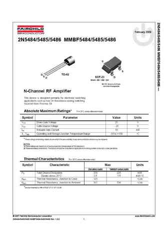
February 2009 2N5484/5485/5486 MMBF5484/5485/5486 2007 Fairchild Semiconductor Corporation www.fairchildsemi.com 2N5484/5485/5486 MMBF5484/5485/5486 Rev. 1.0.0 1 2N5484/5485/5486 MMBF5484/5485/5486 2007 Fairchild Semiconductor Corporation www.fairchildsemi.com Rev. 1.0.0 2 2007 Fairchild Semiconductor Corporation www.fairchildsemi.com Rev. 1.0.0 3 2007
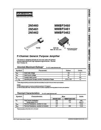
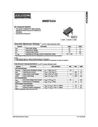
Otros transistores... MMBF4117, MMBF4118, MMBF4119, MMBF4391, MMBF4392, MMBF4393, MMBF4416, MMBF4416A, IRFP064N, MMBF5434, MMBF5457, MMBF5458, MMBF5459, MMBF5460, MMBF5461, MMBF5462, MMBF5484
Parámetros del MOSFET. Cómo se afectan entre sí.
🌐 : EN ES РУ

Liste
Recientemente añadidas las descripciónes de los transistores:
MOSFET: CS95118 | CS85105A | CS75N45 | CS72N12 | CS55N50 | CS48N75A | CS40N27 | MSQ60P04D | MSQ40P07D | MSQ30P40D | MSQ30P15 | MSQ30P07D | MSQ100N03D | MSHM60P14 | MSHM40N085 | MSHM30N46
Popular searches
2n3055 datasheet | 2sc945 | irfp250n | irf9540n | bd139 datasheet | irf9640 | 2n3053 | a1015