2N90 Datasheet. Equivalente. Reemplazo. Hoja de especificaciones. Principales características
Número de Parte: 2N90 📄📄
Tipo de FET: MOSFET
Polaridad de transistor: N
ESPECIFICACIONES MÁXIMAS
Pdⓘ - Máxima disipación de potencia: 85 W
|Vds|ⓘ - Voltaje máximo drenador-fuente: 900 V
|Vgs|ⓘ - Voltaje máximo fuente-puerta: 30 V
|Id|ⓘ - Corriente continua de drenaje: 2.2 A
Tjⓘ - Temperatura máxima de unión: 150 °C
CARACTERÍSTICAS ELÉCTRICAS
trⓘ - Tiempo de subida: 35 nS
Cossⓘ - Capacitancia de salida: 45 pF
RDSonⓘ - Resistencia estado encendido drenaje a fuente: 5.6 Ohm
📄📄 Copiar
Búsqueda de reemplazo de 2N90 MOSFET
- Selecciónⓘ de transistores por parámetros
2N90 datasheet
2n90.pdf

UNISONIC TECHNOLOGIES CO., LTD 2N90 Power MOSFET 2A, 900V N-CHANNEL POWER MOSFET 1 TO-252 DESCRIPTION The UTC 2N90 is an N-channel mode power MOSFET using UTC s advanced technology to provide costumers with planar stripe and DMOS technology. This technology specialized in allowing a 1 minimum on-state resistance and superior switching performance. It TO-251 also can wi
fqu2n90.pdf

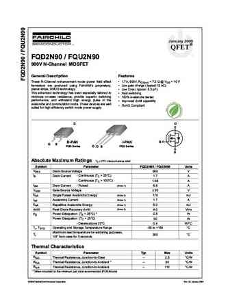
January 2014 FQD2N90 / FQU2N90 N-Channel QFET MOSFET 900 V, 1.7 A, 7.2 Description Features This N-Channel enhancement mode power MOSFET is 1.7 A, 900 V, RDS(on) = 7.2 (Max.) @ VGS = 10 V, produced using Fairchild Semiconductor s proprietary ID = 0.85 A planar stripe and DMOS technology. This advanced Low Gate Charge (Typ. 12 nC) MOSFET technology has been especiall
fqpf2n90.pdf
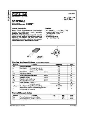
April 2000 TM QFET QFET QFET QFET 900V N-ChanneI MOSFET GeneraI Description Features These N-Channel enhancement mode power field effect 1.4A, 900V, RDS(on) = 7.2 @ VGS = 10 V transistors are produced using Fairchild s proprietary, Low gate charge ( typical 12 nC) planar stripe, DMOS technology. Low Crss ( typical 5.5 pF) This advanced technology has be
fqd2n90tf fqd2n90tm fqd2n90 fqu2n90 fqu2n90tu.pdf
January 2009 QFET FQD2N90 / FQU2N90 900V N-ChanneI MOSFET GeneraI Description Features These N-Channel enhancement mode power field effect 1.7A, 900V, RDS(on) = 7.2 @ VGS = 10 V transistors are produced using Fairchild s proprietary, Low gate charge ( typical 12 nC) planar stripe, DMOS technology. Low Crss ( typical 5.5 pF) This advanced technology has been especi
fqb2n90tm fqi2n90tu.pdf
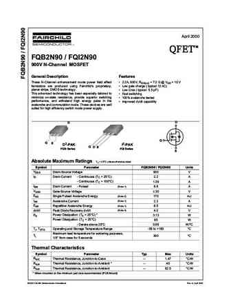
April 2000 TM QFET QFET QFET QFET FQB2N90 / FQI2N90 900V N-ChanneI MOSFET GeneraI Description Features These N-Channel enhancement mode power field effect 2.2A, 900V, RDS(on) = 7.2 @ VGS = 10 V transistors are produced using Fairchild s proprietary, Low gate charge ( typical 12 nC) planar stripe, DMOS technology. Low Crss ( typical 5.5 pF) This advanced technolo
fqp2n90.pdf
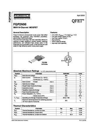
April 2000 TM QFET QFET QFET QFET 900V N-ChanneI MOSFET GeneraI Description Features These N-Channel enhancement mode power field effect 2.2A, 900V, RDS(on) = 7.2 @ VGS = 10 V transistors are produced using Fairchild s proprietary, Low gate charge ( typical 12 nC) planar stripe, DMOS technology. Low Crss ( typical 5.5 pF) This advanced technology has bee
sss2n90a.pdf
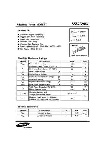
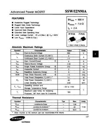
Advanced Power MOSFET FEATURES BVDSS = 900 V Avalanche Rugged Technology RDS(on) = 7.0 Rugged Gate Oxide Technology Lower Input Capacitance ID = 1.5 A Improved Gate Charge Extended Safe Operating Area Lower Leakage Current 25 A (Max.) @ VDS = 900V Low RDS(ON) 5.838 (Typ.) 1 2 3 1.Gate 2. Drain 3. Source Absolute Maximum Ratings Symbol Characteristic Valu
ssp2n90a.pdf

Advanced Power MOSFET FEATURES BVDSS = 900 V Avalanche Rugged Technology RDS(on) = 7.0 Rugged Gate Oxide Technology Lower Input Capacitance ID = 2 A Improved Gate Charge Extended Safe Operating Area Lower Leakage Current 25 A (Max.) @ VDS = 900V Low RDS(ON) 5.838 (Typ.) 1 2 3 1.Gate 2. Drain 3. Source Absolute Maximum Ratings Symbol Characteristic Va
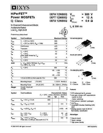
ixfh12n90q ixft12n90q.pdf
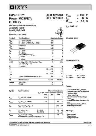
IXFH 12N90Q VDSS = 900 V HiPerFETTM IXFT 12N90Q ID25 = 12 A Power MOSFETs RDS(on) = 0.9 W Q Class N-Channel Enhancement Mode trr 200 ns Avalanche Rated Low Qg, High dv/dt Preliminary data sheet Symbol Test Conditions Maximum Ratings TO-247 AD (IXFH) VDSS TJ = 25 C to 150 C 900 V VDGR TJ = 25 C to 150 C; RGS = 1 MW 900 V VGS Continuous 20 V VGSM Transient 30 V ID25 TC
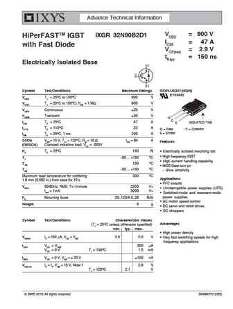
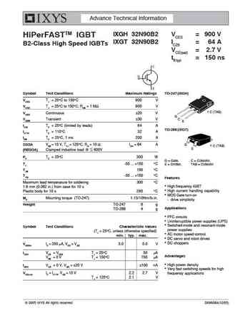
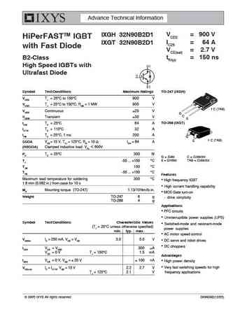
ixgh32n90b2d1 ixgt32n90b2d1.pdf

Advance Technical Information VCES = 900 V IXGH 32N90B2D1 HiPerFASTTM IGBT IC25 = 64 A IXGT 32N90B2D1 with Fast Diode VCE(sat) = 2.7 V tfi typ = 150 ns B2-Class High Speed IGBTs with Ultrafast Diode Symbol Test Conditions Maximum Ratings TO-247 (IXGH) VCES TJ = 25 C to 150 C 900 V VCGR TJ = 25 C to 150 C; RGE = 1 MW 900 V C (TAB) VGES Continuous 20 V G C VGEM Transient
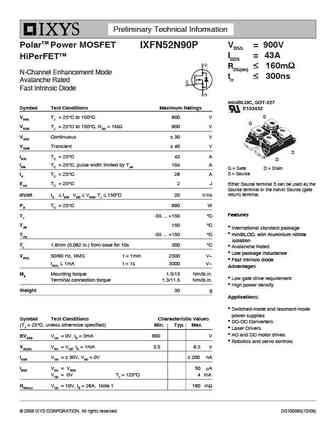
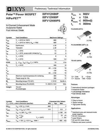
ixfb52n90p.pdf
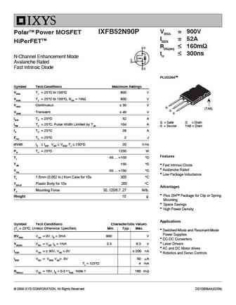
VDSS = 900V IXFB52N90P PolarTM Power MOSFET ID25 = 52A HiPerFETTM RDS(on) 160m trr 300ns N-Channel Enhancement Mode Avalanche Rated Fast Intrinsic Diode PLUS264TM Symbol Test Conditions Maximum Ratings VDSS TJ = 25 C to 150 C 900 V VDGR TJ = 25 C to 150 C, RGS = 1M 900 V VGSS Continuous 30 V G (TAB) D VGSM
ixgx12n90c.pdf

HiPerFASTTM IGBT IXGH 12N90C VCES = 900 V LightspeedTM Series IXGX 12N90C IC25 = 24 A VCES(sat) = 3.0 V tfi(typ) = 70 ns Symbol Test Conditions Maximum Ratings TO-247 (IXGH) VCES TJ = 25 C to 150 C 900 V VCGR TJ = 25 C to 150 C; RGE = 1 M 900 V VGES Continuous 20 V C (TAB) VGEM Transient 30 V G C E IC25 TC = 25 C24 A IC90 TC = 90 C12 A PLUS 247 (IXGX) ICM TC = 25
ixgr32n90b2d1.pdf
Advance Technical Information VCES = 900 V IXGR 32N90B2D1 HiPerFASTTM IGBT IC25 = 47 A with Fast Diode VCE(sat) = 2.9 V tfi typ = 150 ns Electrically Isolated Base Symbol Test Conditions Maximum Ratings ISOPLUS247 (IXGR) E153432 VCES TJ = 25OC to 150OC 900 V VCGR TJ = 25OC to 150OC; RGE = 1 M 900 V VGES Continuous 20 V VGEM Transient 30 V G C IC25 TC = 25OC47 A ISOLATED T
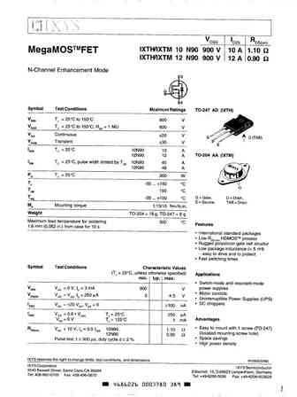
ixfh10n90 ixfm10n90 ixfh12n90 ixfm12n90 ixfh13n90 ixfm13n90.pdf
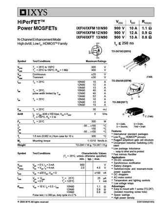
VDSS ID25 RDS(on) HiPerFETTM IXFH/IXFM 10 N90 900 V 10 A 1.1 Power MOSFETs IXFH/IXFM 12 N90 900 V 12 A 0.9 IXFH/IXFT 13 N90 900 V 13 A 0.8 N-Channel Enhancement Mode 250 ns High dv/dt, Low trr, HDMOSTM Family trr TO-247 AD (IXFH) Symbol Test Conditions Maximum Ratings VDSS TJ = 25 C to 1
ixgh32n90b2 ixgt32n90b2.pdf
Advance Technical Information IXGH 32N90B2 VCES = 900 V HiPerFASTTM IGBT IXGT 32N90B2 IC25 = 64 A B2-Class High Speed IGBTs VCE(sat) = 2.7 V tfi typ = 150 ns Symbol Test Conditions Maximum Ratings TO-247 (IXGH) VCES TJ = 25 C to 150 C 900 V VCGR TJ = 25 C to 150 C; RGE = 1 M 900 V C (TAB) VGES Continuous 20 V G VGEM Transient 30 V C E IC25 TC = 25 C (limited by leads)
ixgh12n90c.pdf
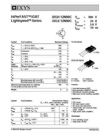
HiPerFASTTM IGBT IXGH 12N90C VCES = 900 V LightspeedTM Series IXGX 12N90C IC25 = 24 A VCES(sat) = 3.0 V tfi(typ) = 70 ns Symbol Test Conditions Maximum Ratings TO-247 (IXGH) VCES TJ = 25 C to 150 C 900 V VCGR TJ = 25 C to 150 C; RGE = 1 M 900 V VGES Continuous 20 V C (TAB) VGEM Transient 30 V G C E IC25 TC = 25 C24 A IC90 TC = 90 C12 A PLUS 247 (IXGX) ICM TC = 25
ixfn52n90p.pdf
Preliminary Technical Information PolarTM Power MOSFET VDSS = 900V IXFN52N90P ID25 = 43A HiPerFETTM RDS(on) 160m N-Channel Enhancement Mode trr 300ns Avalanche Rated Fast Intrinsic Diode miniBLOC, SOT-227 Symbol Test Conditions Maximum Ratings E153432 S VDSS TJ = 25 C to 150 C 900 V G VDGR TJ = 25 C to 150 C, RGS
ixfk32n90p ixfx32n90p.pdf
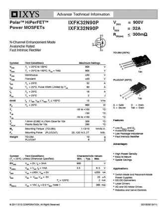
Advance Technical Information PolarTM HiPerFETTM VDSS = 900V IXFK32N90P Power MOSFETs ID25 = 32A IXFX32N90P RDS(on)
ixgt32n90b2d1.pdf

Advance Technical Information VCES = 900 V IXGH 32N90B2D1 HiPerFASTTM IGBT IC25 = 64 A IXGT 32N90B2D1 with Fast Diode VCE(sat) = 2.7 V tfi typ = 150 ns B2-Class High Speed IGBTs with Ultrafast Diode Symbol Test Conditions Maximum Ratings TO-247 (IXGH) VCES TJ = 25 C to 150 C 900 V VCGR TJ = 25 C to 150 C; RGE = 1 MW 900 V C (TAB) VGES Continuous 20 V G C VGEM Transient
ixfh12n90p ixfv12n90p-s.pdf
Preliminary Technical Information IXFH12N90P VDSS = 900V PolarTM Power MOSFET IXFV12N90P ID25 = 12A HiPerFETTM RDS(on) 900m IXFV12N90PS trr 300ns N-Channel Enhancement Mode Avalanche Rated PLUS220 (IXFV) Fast Intrinsic Diode G Symbol Test Conditions Maximum Ratings D S VDSS TJ = 25 C to 150 C 900 V D (TAB) VDGR TJ
ixgt32n90b2.pdf

Advance Technical Information IXGH 32N90B2 VCES = 900 V HiPerFASTTM IGBT IXGT 32N90B2 IC25 = 64 A B2-Class High Speed IGBTs VCE(sat) = 2.7 V tfi typ = 150 ns Symbol Test Conditions Maximum Ratings TO-247 (IXGH) VCES TJ = 25 C to 150 C 900 V VCGR TJ = 25 C to 150 C; RGE = 1 M 900 V C (TAB) VGES Continuous 20 V G VGEM Transient 30 V C E IC25 TC = 25 C (limited by leads)
ixgh32n90b2d1.pdf
Advance Technical Information VCES = 900 V IXGH 32N90B2D1 HiPerFASTTM IGBT IC25 = 64 A IXGT 32N90B2D1 with Fast Diode VCE(sat) = 2.7 V tfi typ = 150 ns B2-Class High Speed IGBTs with Ultrafast Diode Symbol Test Conditions Maximum Ratings TO-247 (IXGH) VCES TJ = 25 C to 150 C 900 V VCGR TJ = 25 C to 150 C; RGE = 1 MW 900 V C (TAB) VGES Continuous 20 V G C VGEM Transient
ixgh32n90b2.pdf

Advance Technical Information IXGH 32N90B2 VCES = 900 V HiPerFASTTM IGBT IXGT 32N90B2 IC25 = 64 A B2-Class High Speed IGBTs VCE(sat) = 2.7 V tfi typ = 150 ns Symbol Test Conditions Maximum Ratings TO-247 (IXGH) VCES TJ = 25 C to 150 C 900 V VCGR TJ = 25 C to 150 C; RGE = 1 M 900 V C (TAB) VGES Continuous 20 V G VGEM Transient 30 V C E IC25 TC = 25 C (limited by leads)
fqd2n90 fqu2n90.pdf
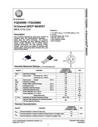
FQD2N90 / FQU2N90 N-Channel QFET MOSFET 900 V, 1.7 A, 7.2 Features 1.7 A, 900 V, RDS(on) = 7.2 (Max.) @ VGS = 10 V, ID = 0.85 A Description Low Gate Charge (Typ. 12 nC) This N-Channel enhancement mode power MOSFET is Low Crss (Typ. 5.5 pF) produced using ON Semiconductor s proprietary 100% Avalanche Tested planar stripe and DMOS technology. This advanced
fqp2n90.pdf

Is Now Part of To learn more about ON Semiconductor, please visit our website at www.onsemi.com Please note As part of the Fairchild Semiconductor integration, some of the Fairchild orderable part numbers will need to change in order to meet ON Semiconductor s system requirements. Since the ON Semiconductor product management systems do not have the ability to manage part nomenclatur
12n90.pdf

UNISONIC TECHNOLOGIES CO., LTD 12N90 Power MOSFET 12A, 900V N-CHANNEL POWER MOSFET DESCRIPTION The UTC 12N90 is an N-channel enhancement mode power MOSFET useing UTC s advanced technology to provide customers with planar stripe and DMOS technology. This technology is specialized in allowing a minimum on-state resistance and superior switching performance. It also can with
2n90l-ta3-t 2n90g-ta3-t 2n90l-tf3-t 2n90g-tf3-t 2n90l-tm3-t 2n90g-tm3-t 2n90l-tn3-r 2n90g-tn3-r 2n90l-tnd-r 2n90g-tnd-r.pdf

UNISONIC TECHNOLOGIES CO., LTD 2N90 Power MOSFET 2A, 900V N-CHANNEL POWER MOSFET DESCRIPTION The UTC 2N90 is an N-channel mode power MOSFET using UTC s advanced technology to provide costumers with planar stripe and DMOS technology. This technology specialized in allowing a minimum on-state resistance and superior switching performance. It also can withstand high energy
ap02n90h.pdf
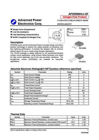
AP02N90H/J-HF Halogen-Free Product Advanced Power N-CHANNEL ENHANCEMENT MODE Electronics Corp. POWER MOSFET Simple Drive Requirement BVDSS 900V D Low On-resistance RDS(ON) 7.2 Fast Switching Characteristics ID 1.9A RoHS Compliant & Halogen-Free G S Description AP02N90 series are from Advanced Power innovated design and silicon G process technology to achieve the
ap02n90i.pdf
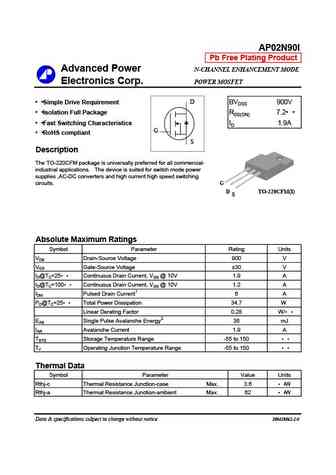
AP02N90I Pb Free Plating Product Advanced Power N-CHANNEL ENHANCEMENT MODE Electronics Corp. POWER MOSFET Simple Drive Requirement D BVDSS 900V Isolation Full Package RDS(ON) 7.2 Fast Switching Characteristics ID 1.9A G RoHS compliant S Description The TO-220CFM package is universally preferred for all commercial- industrial applications. The device is suited for s
ap02n90p-hf.pdf
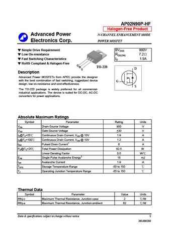
AP02N90P-HF Halogen-Free Product Advanced Power N-CHANNEL ENHANCEMENT MODE Electronics Corp. POWER MOSFET Simple Drive Requirement BVDSS 900V Low On-resistance RDS(ON) 7.2 Fast Switching Characteristics ID 1.9A RoHS Compliant & Halogen-Free G D TO-220 D S Description Advanced Power MOSFETs from APEC provide the designer with the best combination of fast switching
ap02n90p.pdf
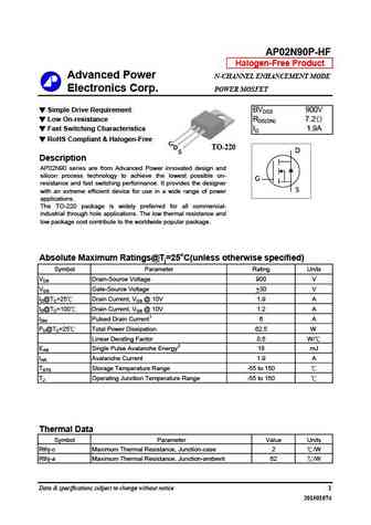
AP02N90P-HF Halogen-Free Product Advanced Power N-CHANNEL ENHANCEMENT MODE Electronics Corp. POWER MOSFET Simple Drive Requirement BVDSS 900V Low On-resistance RDS(ON) 7.2 Fast Switching Characteristics ID 1.9A RoHS Compliant & Halogen-Free G D TO-220 D S Description AP02N90 series are from Advanced Power innovated design and silicon process technology to achieve
ap02n90jb.pdf
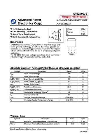
AP02N90JB Halogen-Free Product Advanced Power N-CHANNEL ENHANCEMENT MODE Electronics Corp. POWER MOSFET 100% Avalanche Test BVDSS 900V D Fast Switching Characteristic RDS(ON) 7.2 Simple Drive Requirement ID 1.9A RoHS Compliant & Halogen-Free G S Description AP02N90 series are from Advanced Power innovated design and silicon process technology to achieve the lowest
ap02n90h-hf ap02n90j-hf.pdf
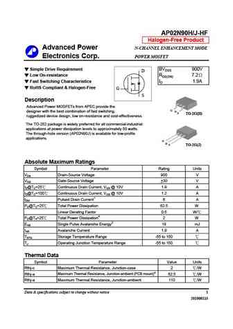
AP02N90H/J-HF Halogen-Free Product Advanced Power N-CHANNEL ENHANCEMENT MODE Electronics Corp. POWER MOSFET Simple Drive Requirement BVDSS 900V D Low On-resistance RDS(ON) 7.2 Fast Switching Characteristics ID 1.9A RoHS Compliant & Halogen-Free G S Description Advanced Power MOSFETs from APEC provide the G designer with the best combination of fast switching, D
ap02n90i-hf.pdf
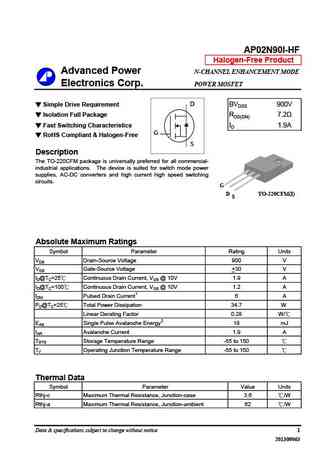
AP02N90I-HF Halogen-Free Product Advanced Power N-CHANNEL ENHANCEMENT MODE Electronics Corp. POWER MOSFET Simple Drive Requirement D BVDSS 900V Isolation Full Package RDS(ON) 7.2 Fast Switching Characteristics ID 1.9A G RoHS Compliant & Halogen-Free S Description The TO-220CFM package is universally preferred for all commercial- industrial applications. The device
ap02n90j.pdf

AP02N90H/J-HF Halogen-Free Product Advanced Power N-CHANNEL ENHANCEMENT MODE Electronics Corp. POWER MOSFET Simple Drive Requirement BVDSS 900V D Low On-resistance RDS(ON) 7.2 Fast Switching Characteristics ID 1.9A RoHS Compliant & Halogen-Free G S Description AP02N90 series are from Advanced Power innovated design and silicon G process technology to achieve the
pj2n9014.pdf
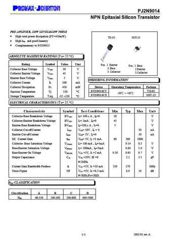
PJ2N9014 NPN Epitaxial Silicon Transistor PRE-APLIFIER, LOW LEVEL&LOW NOISE High total power dissipation (PT=450mW) TO-92 SOT-23 High h and good linearity FE Complementary to PJ2N9015 ABSOLUTE MAXIMUM RATINGS (Ta= 25 C) Rating Symbol Value Uint Pin 1. Emitter Pin 1. Base 2. Base Collector Base Voltage V 50 V 2.Emitter CBO 3. Collector 3.Collector
ptf12n90.pdf
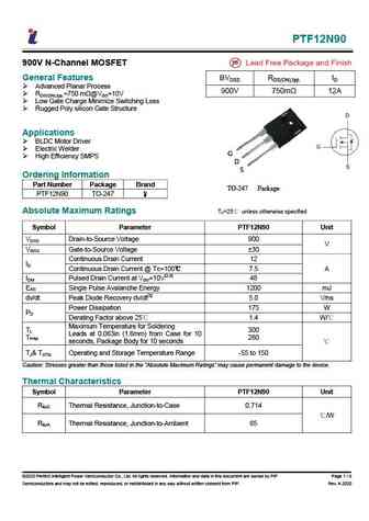
PTF12N90 900V N-Channel MOSFET General Features BVDSS RDS(ON),typ. ID Advanced Planar Process 900V 750m 12A RDS(ON),typ.=750 m @VGS=10V Low Gate Charge Minimize Switching Loss Rugged Poly silicon Gate Structure Applications BLDC Motor Driver Electric Welder G High Efficiency SMPS D S Ordering Information Part Number Package Brand TO-247 Package PT
swf2n90k2.pdf
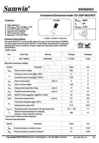
SW2N90K2 N-channel Enhanced mode TO-220F MOSFET TO-220F BVDSS 900V Features ID 2A High ruggedness RDS(ON) 2.2 Low RDS(ON) (Typ 2.2 )@VGS=10V Low Gate Charge (Typ 13nC) 2 Improved dv/dt Capability 1 100% Avalanche Tested 2 1 3 Application UPS,LED,SMPS 1. Gate 2. Drain 3. Source 3 General Description This power MOSFET is
hfd2n90.pdf
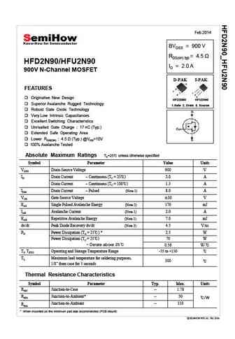
Feb 2014 BVDSS = 900 V RDS(on) typ HFD2N90/HFU2N90 ID = 2.0 A 900V N-Channel MOSFET D-PAK I-PAK 2 FEATURES 1 1 3 2 3 Originative New Design HFD2N90 HFU2N90 Superior Avalanche Rugged Technology 1.Gate 2. Drain 3. Source Robust Gate Oxide Technology Very Low Intrinsic Capacitances Excellent Switching Characteristics Unrivalled Gate Charge 17 nC (Typ.)
hfp2n90.pdf
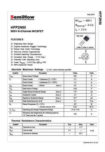
Feb 2014 BVDSS = 900 V RDS(on) typ HFP2N90 ID = 2.2 A 900V N-Channel MOSFET TO-220 FEATURES Originative New Design 1 2 3 Superior Avalanche Rugged Technology 1.Gate 2. Drain 3. Source Robust Gate Oxide Technology Very Low Intrinsic Capacitances Excellent Switching Characteristics Unrivalled Gate Charge 17 nC (Typ.) Extended Safe Operating Area Lower
hfs2n90.pdf
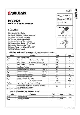
Feb 2014 BVDSS = 900 V RDS(on) typ HFS2N90 ID = 2.2 A 900V N-Channel MOSFET TO-220F FEATURES 1 1 Originative New Design 2 3 Superior Avalanche Rugged Technology 1.Gate 2. Drain 3. Source Robust Gate Oxide Technology Very Low Intrinsic Capacitances Excellent Switching Characteristics Unrivalled Gate Charge 17 nC (Typ.) Extended Safe Operating Area
cs2n90f cs2n90p cs2n90b.pdf
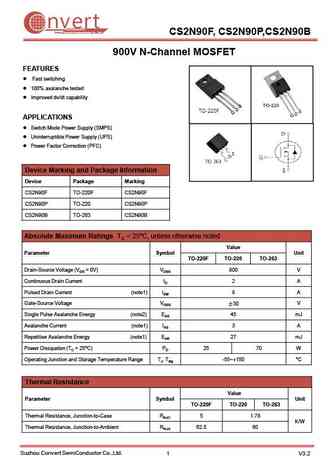
nvert Suzhou Convert Semiconductor Co ., Ltd. CS2N90F, CS2N90P,CS2N90B 900V N-Channel MOSFET FEATURES Fast switching 100% avalanche tested Improved dv/dt capability APPLICATIONS Switch Mode Power Supply (SMPS) Uninterruptible Power Supply (UPS) Power Factor Correction (PFC) Device Marking and Package Information Device Package Marking CS2N90F TO-220F CS2N90
sfp055n90c3 sfb052n90c3.pdf
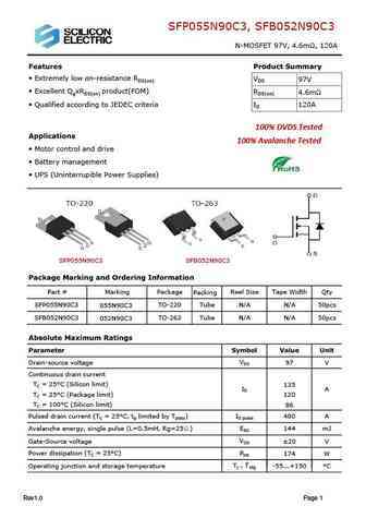
SFP055N90C3, SFB052N90C3 N-MOSFET 97V, 4.6m , 120A Features Product Summary Extremely low on-resistance RDS(on) VDS 97V Excellent QgxRDS(on) product(FOM) RDS(on) 4.6m Qualified according to JEDEC criteria ID 120A 100% DVDS Tested Applications 100% Avalanche Tested Motor control and drive 100% Avalanche Tested 100% Avalanche Tested Battery management
Otros transistores... 8N90, 9N90, 10N90, 11N90, 12N90, 9N95, 9N100, 1N90, IRF3710, 3N90, 4N90, 5N90, 6N90, 7N90, 1N80, 2N80, 3N80
Parámetros del MOSFET. Cómo se afectan entre sí.
🌐 : EN ES РУ

Liste
Recientemente añadidas las descripciónes de los transistores:
MOSFET: MSQ60P04D | MSQ40P07D | MSQ30P40D | MSQ30P15 | MSQ30P07D | MSQ100N03D | MSHM60P14 | MSHM40N085 | MSHM30N46 | MSH60N35D | MSH40N032 | MSH30P100 | MSH100N045SA | MSD60P16 | MSD40P45 | MSB100N023
Popular searches
2n3638 | tip127 datasheet | irlz24n | irf620 | irfp350 | 13003 transistor | c458 transistor | 2sc1775