4N90 MOSFET Equivalente. Reemplazo. Hoja de especificaciones. Principales características
Número de Parte: 4N90
Tipo de FET: MOSFET
Polaridad de transistor: N
ESPECIFICACIONES MÁXIMAS
Pdⓘ - Máxima disipación de potencia: 140 W
|Vds|ⓘ - Voltaje máximo drenador-fuente: 900 V
|Vgs|ⓘ - Voltaje máximo fuente-puerta: 30 V
|Id|ⓘ - Corriente continua de drenaje: 4 A
Tjⓘ - Temperatura máxima de unión: 150 °C
CARACTERÍSTICAS ELÉCTRICAS
trⓘ - Tiempo de subida: 50 nS
Cossⓘ - Capacitancia de salida: 65 pF
RDSonⓘ - Resistencia estado encendido drenaje a fuente: 3.5 Ohm
Encapsulados: TO-220F TO-220F1 TO-220 TO-252 TO-262
Búsqueda de reemplazo de 4N90 MOSFET
- Selecciónⓘ de transistores por parámetros
4N90 datasheet
4n90.pdf
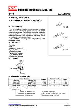
UNISONIC TECHNOLOGIES CO., LTD 4N90 Power MOSFET 4 Amps, 900 Volts N-CHANNEL POWER MOSFET 1 DESCRIPTION TO-252 The UTC 4N90 is a N-channel enhancement MOSFET adopting UTC s advanced technology to provide customers with DMOS, planar stripe technology. This technology is designed to meet the requirements of the minimum on-state resistance and perfect switching performance.
ste24n90 ste36n50-da ste36n50-dk ste38n60 ste38na50 ste45n50 ste50n40 ste90n25.pdf
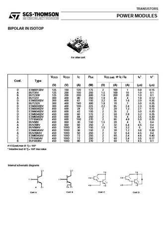
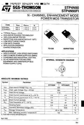
TRANSISTORS POWER MODULES BIPOLAR IN ISOTOP For other conf. VCEO VCEV IC Ptot VCE (sat) @IC / IB ts* tf* Conf. Type (V) (V) (A) (W) (V) (A) (A) ( s) ( s) D ESM2012DV 125 150 120 175 2 100 1 0.9 0.15 A BUT30V 125 200 100 250 1.5 100 10 1.0 0.1 B BUT230V 125 200 200 300 1.9 200 20 1.0 0.1 A BUT32V 300 400 80 250 1.9 40 4 1.9 0.12 D ESM2030DV 300 400 67 150 2.2 56 1.6 2.0 0.35 B BUT2
stf4n90k5.pdf
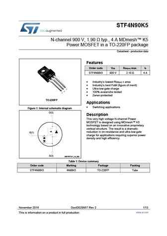
STF4N90K5 N-channel 900 V, 1.90 typ., 4 A MDmesh K5 Power MOSFET in a TO-220FP package Datasheet - production data Features Order code V R max. I DS DS(on) D STF4N90K5 900 V 2.10 4 A Industry s lowest R x area DS(on) Industry s best FoM (figure of merit) Ultra-low gate charge 100% avalanche tested Zener-protected TO-220FP Applications
stp4n90k5.pdf
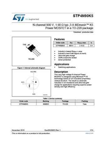
STP4N90K5 N-channel 900 V, 1.90 typ.,3 A MDmesh K5 Power MOSFET in a TO-220 package Datasheet - production data Features Order code V R max. I DS DS(on) D TAB STP4N90K5 900 V 2.10 3 A Industry s lowest R x area DS(on) Industry s best FoM (figure of merit) 3 2 Ultra-low gate charge 1 100% avalanche tested TO-220 Zener-protected Appl
std4n90k5.pdf
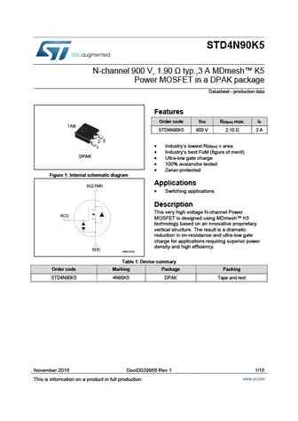
STD4N90K5 N-channel 900 V, 1.90 typ.,3 A MDmesh K5 Power MOSFET in a DPAK package Datasheet - production data Features Order code V R max. I DS DS(on) D STD4N90K5 900 V 2.10 3 A Industry s lowest R x area DS(on) Industry s best FoM (figure of merit) Ultra-low gate charge 100% avalanche tested Zener-protected Figure 1 Internal schematic
fqi4n90.pdf
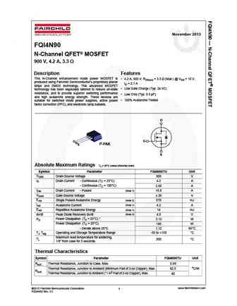
November 2013 FQI4N90 N-Channel QFET MOSFET 900 V, 4.2 A, 3.3 Description Features This N-Channel enhancement mode power MOSFET is 4.2 A, 900 V, RDS(on) = 3.3 (Max.) @ VGS = 10 V, produced using Fairchild Semiconductor s proprietary planar ID = 2.1 A stripe and DMOS technology. This advanced MOSFET Low Gate Charge (Typ. 24 nC) technology has been especially tai
ssh4n90.pdf
This Material Copyrighted By Its Respective Manufacturer This Material Copyrighted By Its Respective Manufacturer This Material Copyrighted By Its Respective Manufacturer This Material Copyrighted By Its Respective Manufacturer This Material Copyrighted By Its Respective Manufacturer This Material Copyrighted By Its Respective Manufacturer
fqb4n90tm fqi4n90tu.pdf
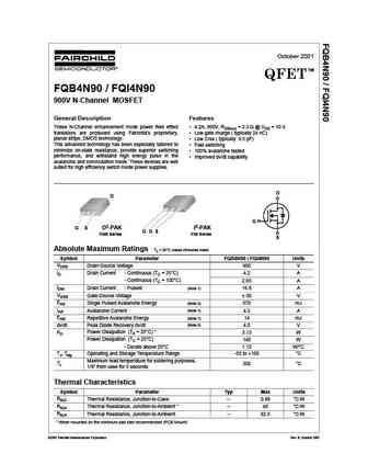
October 2001 TM QFET FQB4N90 / FQI4N90 900V N-Channel MOSFET General Description Features These N-Channel enhancement mode power field effect 4.2A, 900V, RDS(on) = 3.3 @ VGS = 10 V transistors are produced using Fairchild s proprietary, Low gate charge ( typically 24 nC) planar stripe, DMOS technology. Low Crss ( typically 9.5 pF) This advanced technology has been es
fqp4n90c fqpf4n90c.pdf
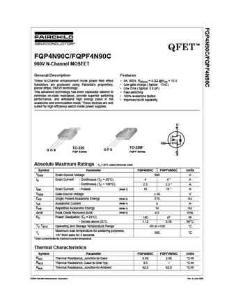
TM QFET FQP4N90C/FQPF4N90C 900V N-Channel MOSFET General Description Features These N-Channel enhancement mode power field effect 4A, 900V, RDS(on) = 4.2 @VGS = 10 V transistors are produced using Fairchild s proprietary, Low gate charge ( typical 17nC) planar stripe, DMOS technology. Low Crss ( typical 5.6 pF) This advanced technology has been especially tailored to
fqpf4n90.pdf
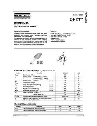
October 2001 TM QFET FQPF4N90 900V N-Channel MOSFET General Description Features These N-Channel enhancement mode power field effect 2.5A, 900V, RDS(on) = 3.3 @ VGS = 10 V transistors are produced using Fairchild s proprietary, Low gate charge ( typically 24 nC) planar stripe, DMOS technology. Low Crss ( typically 9.5 pF) This advanced technology has been especially
fqp4n90.pdf
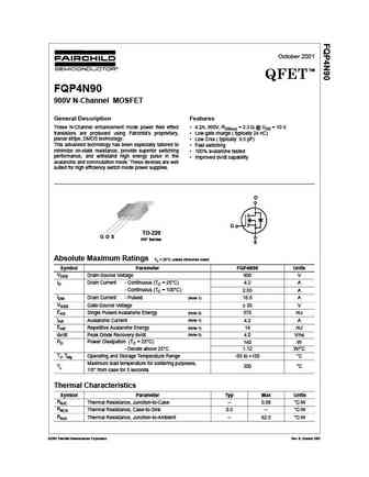
October 2001 TM QFET FQP4N90 900V N-Channel MOSFET General Description Features These N-Channel enhancement mode power field effect 4.2A, 900V, RDS(on) = 3.3 @ VGS = 10 V transistors are produced using Fairchild s proprietary, Low gate charge ( typically 24 nC) planar stripe, DMOS technology. Low Crss ( typically 9.5 pF) This advanced technology has been especially t
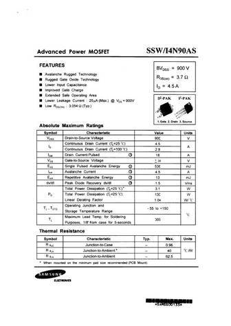
sss4n90a.pdf

Advanced Power MOSFET FEATURES BVDSS = 900 V Avalanche Rugged Technology RDS(on) = 5.0 Rugged Gate Oxide Technology Lower Input Capacitance ID = 2.5 A Improved Gate Charge Extended Safe Operating Area Lower Leakage Current 25 A (Max.) @ VDS = 900V Low RDS(ON) 4.181 (Typ.) 1 2 3 1.Gate 2. Drain 3. Source Absolute Maximum Ratings Symbol Characteristic Valu
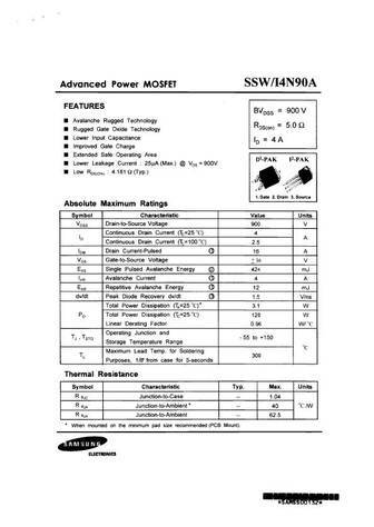
sss4n90as.pdf
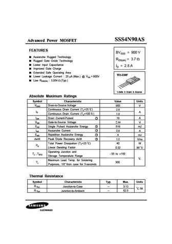
Advanced Power MOSFET FEATURES BVDSS = 900 V Avalanche Rugged Technology RDS(on) = 3.7 Rugged Gate Oxide Technology Lower Input Capacitance ID = 2.8 A Improved Gate Charge Extended Safe Operating Area Lower Leakage Current 25 A (Max.) @ VDS = 900V Low RDS(ON) 3.054 (Typ.) 1 2 3 1.Gate 2. Drain 3. Source Absolute Maximum Ratings Symbol Characteristic Valu
ssp4n90a.pdf
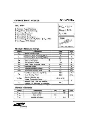
Advanced Power MOSFET FEATURES BVDSS = 900 V Avalanche Rugged Technology RDS(on) = 5.0 Rugged Gate Oxide Technology Lower Input Capacitance ID = 4 A Improved Gate Charge Extended Safe Operating Area Lower Leakage Current 25 A (Max.) @ VDS = 900V Low RDS(ON) 4.181 (Typ.) 1 2 3 1.Gate 2. Drain 3. Source Absolute Maximum Ratings Symbol Characteristic Value
ssp4n90as.pdf
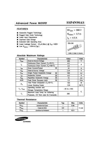
SSP4N90AS Advanced Power MOSFET FEATURES BVDSS = 900 V Avalanche Rugged Technology RDS(on) = 3.7 Rugged Gate Oxide Technology Lower Input Capacitance ID = 4.5 A Improved Gate Charge Extended Safe Operating Area TO-220 Lower Leakage Current 25 A (Max.) @ VDS = 900V Low RDS(ON) 3.054 (Typ.) 1 2 3 1.Gate 2. Drain 3. Source Absolute Maximum Ratings Symbol Ch
ssf4n90as.pdf
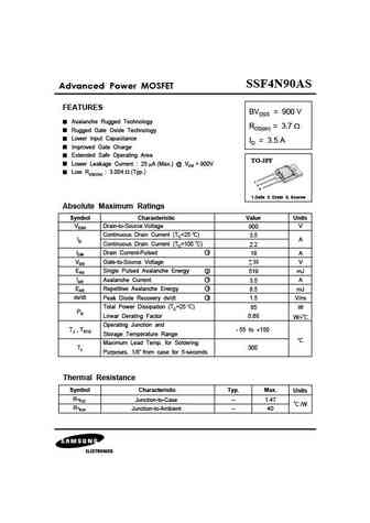
SSF4N90AS Advanced Power MOSFET FEATURES BVDSS = 900 V Avalanche Rugged Technology RDS(on) = 3.7 Rugged Gate Oxide Technology Lower Input Capacitance ID = 3.5 A Improved Gate Charge Extended Safe Operating Area TO-3PF Lower Leakage Current 25 A (Max.) @ VDS = 900V Low RDS(ON) 3.054 (Typ.) 1 2 3 1.Gate 2. Drain 3. Source Absolute Maximum Ratings Symbol Ch
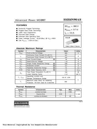
ssh4n90as.pdf
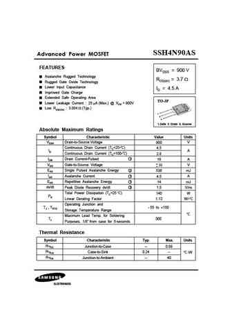
SSH4N90AS Advanced Power MOSFET FEATURES BVDSS = 900 V Avalanche Rugged Technology RDS(on) = 3.7 Rugged Gate Oxide Technology Lower Input Capacitance ID = 4.5 A Improved Gate Charge Extended Safe Operating Area TO-3P Lower Leakage Current 25 A (Max.) @ VDS = 900V Low RDS(ON) 3.054 (Typ.) 1 2 3 1.Gate 2. Drain 3. Source Absolute Maximum Ratings Symbol Cha
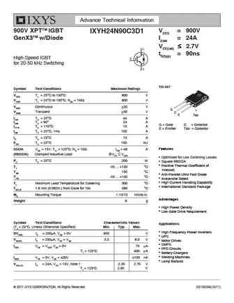
ixyh24n90c3.pdf
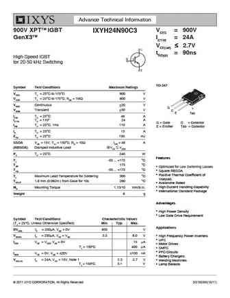
Advance Technical Information 900V XPTTM IGBT VCES = 900V IXYH24N90C3 GenX3TM IC110 = 24A VCE(sat) 2.7V tfi(typ) = 90ns High-Speed IGBT for 20-50 kHz Switching TO-247 Symbol Test Conditions Maximum Ratings VCES TJ = 25 C to 175 C 900 V VCGR TJ = 25 C to 175 C, RGE = 1M 900 V VGES Continuous 20 V G VGEM Transient 30 V C E Tab IC25 TC = 25
ixft24n90p ixfh24n90p.pdf
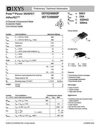
Preliminary Technical Information VDSS = 900V IXFH24N90P PolarTM Power MOSFET ID25 = 24A IXFT24N90P HiPerFETTM RDS(on) 420m N-Channel Enhancement Mode trr 300ns Avalanche Rated Fast Intrinsic Diode TO-247 (IXFH) Symbol Test Conditions Maximum Ratings VDSS TJ = 25 C to 150 C 900 V VDGR TJ = 25 C to 150 C, RGS = 1M
ixyh24n90c3d1.pdf
Advance Technical Information 900V XPTTM IGBT VCES = 900V IXYH24N90C3D1 GenX3TM w/Diode IC90 = 24A VCE(sat) 2.7V tfi(typ) = 90ns High-Speed IGBT for 20-50 kHz Switching TO-247 Symbol Test Conditions Maximum Ratings VCES TJ = 25 C to 150 C 900 V VCGR TJ = 25 C to 150 C, RGE = 1M 900 V VGES Continuous 20 V G VGEM Transient 30 V C E Tab IC25
fqp4n90c fqpf4n90c.pdf

Is Now Part of To learn more about ON Semiconductor, please visit our website at www.onsemi.com Please note As part of the Fairchild Semiconductor integration, some of the Fairchild orderable part numbers will need to change in order to meet ON Semiconductor s system requirements. Since the ON Semiconductor product management systems do not have the ability to manage part nomenclatur
4n90l-tf3t-t 4n90g-tf3t-t 4n90l-tm3-t 4n90g-tm3-t 4n90l-tn3-r 4n90g-tn3-r 4n90l-t3n-t 4n90g-t3n-t.pdf

UNISONIC TECHNOLOGIES CO., LTD 4N90 Power MOSFET 4 Amps, 900 Volts N-CHANNEL POWER MOSFET DESCRIPTION The UTC 4N90 is a N-channel enhancement MOSFET adopting UTC s advanced technology to provide customers with DMOS, planar stripe technology. This technology is designed to meet the requirements of the minimum on-state resistance and perfect switching performance. It also ca
4n90l-ta3-t 4n90g-ta3-t 4n90l-tf3-t 4n90g-tf3-t 4n90l-tf1-t 4n90g-tf1-t 4n90l-tf2-t 4n90g-tf2-t.pdf
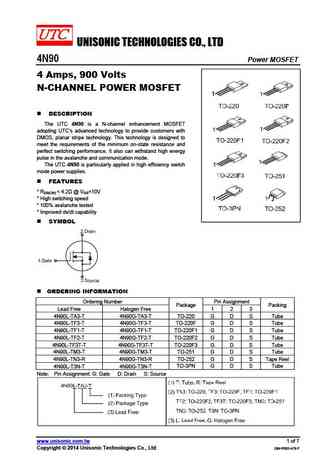
UNISONIC TECHNOLOGIES CO., LTD 4N90 Power MOSFET 4 Amps, 900 Volts N-CHANNEL POWER MOSFET DESCRIPTION The UTC 4N90 is a N-channel enhancement MOSFET adopting UTC s advanced technology to provide customers with DMOS, planar stripe technology. This technology is designed to meet the requirements of the minimum on-state resistance and perfect switching performance. It also ca
tsm4n90ci tsm4n90cz.pdf
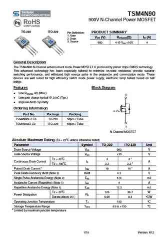
TSM4N90 900V N-Channel Power MOSFET TO-220 ITO-220 PRODUCT SUMMARY Pin Definition 1. Gate VDS (V) RDS(on)( ) ID (A) 2. Drain 3. Source 900 4 @ VGS =10V 4 General Description The TSM4N90 N-Channel enhancement mode Power MOSFET is produced by planar stripe DMOS technology. This advanced technology has been especially tailored to minimize on-state resistance, provide s
aotf4n90.pdf
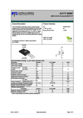
AOTF4N90 900V,4A N-Channel MOSFET General Description Product Summary VDS 1000V@150 The AOTF4N90 is fabricated using an advanced high voltage MOSFET process that is designed to deliver high ID (at VGS=10V) 4A levels of performance and robustness in popular AC-DC RDS(ON) (at VGS=10V)
jcs4n90va jcs4n90ra jcs4n90sa jcs4n90fa jcs4n90ca.pdf
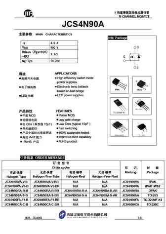
N R N-CHANNEL MOSFET JCS4N90A MAIN CHARACTERISTICS Package ID 4.0 A VDSS 900 V Rdson Vgs=10V 3.3 -MAX Qg-Typ 14.7nC APPLICATIONS High efficiency switch mode . power supplies Electronic lamp ballasts based on half bridge LED power suppli
jcs4n90fh jcs4n90rh jcs4n90vh.pdf
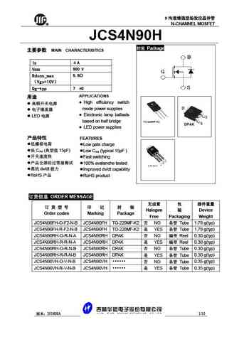
N R N-CHANNEL MOSFET CS J 4N90H Package MAIN CHARACTERISTICS ID 4 4 4A VDSS 900 V Rdson_max 5.5 Vgs=10V Qg-typ 7 nC APPLICATIONS High efficiency switch mode power supplies Electronic lamp ballasts LED based on half bridge
fhf4n90a.pdf
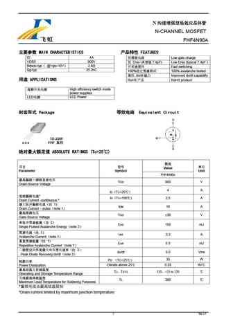
N N-CHANNEL MOSFET FHF4N90A MAIN CHARACTERISTICS FEATURES ID 4A Low gate charge VDSS 900V Crss ( 7.4pF) Low Crss (typical 7.4pF ) Rdson-typ @Vgs=10V 2.6 Fast switching Qg-typ 25.2nC 100% 100% avalanche tested dv/dt Improved dv/
hfs4n90.pdf
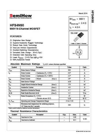
March 2014 BVDSS = 900 V RDS(on) typ HFS4N90 ID = 4.0 A 900V N-Channel MOSFET TO-220F FEATURES 1 1 Originative New Design 2 3 Superior Avalanche Rugged Technology 1.Gate 2. Drain 3. Source Robust Gate Oxide Technology Very Low Intrinsic Capacitances Excellent Switching Characteristics Unrivalled Gate Charge 30 nC (Typ.) Extended Safe Operating Area
hfp4n90.pdf
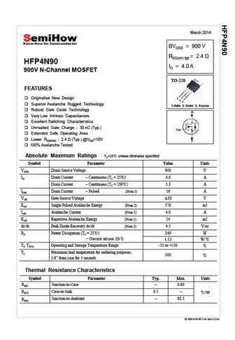
March 2014 BVDSS = 900 V RDS(on) typ HFP4N90 ID = 4.0 A 900V N-Channel MOSFET TO-220 FEATURES Originative New Design 1 2 3 Superior Avalanche Rugged Technology 1.Gate 2. Drain 3. Source Robust Gate Oxide Technology Very Low Intrinsic Capacitances Excellent Switching Characteristics Unrivalled Gate Charge 30 nC (Typ.) Extended Safe Operating Area Low
cs64n90f cs64n90 cs64n90b.pdf

CS64N90 Pb CS64N90 Pb Free Plating Product 85V,92A N-Channel Trench Process Power MOSFET General Description CS64N90 (TO-220 HeatSink) CS64N90 series is N-channel MOS Field Effect Transistor designed for high current switching applications. Rugged EAS capability and ultra low RDS(ON) is suitable for PWM, load switching especially for E-Bike controller applications. DS G Fea
dk64n90f dk64n90 dk64n90b.pdf
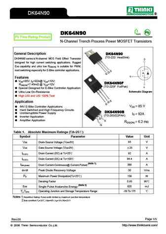
DK64N90 Pb DK64N90 Pb Free Plating Product N-Channel Trench Process Power MOSFET Transistors General Description DK64N90 (TO-220 HeatSink) DK64N90 series is N-channel MOS Field Effect Transistor designed for high current switching applications. Rugged EAS capability and ultra low RDS(ON) is suitable for PWM, load switching especially for E-Bike controller applications. DS G
tmp4n90 tmpf4n90.pdf
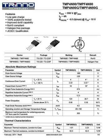
TMP4N90/TMPF4N90 TMP4N90G/TMPF4N90G VDSS = 990 V @Tjmax Features ID = 4A Low gate charge RDS(ON) = 4.0 W(max) @ VGS= 10 V 100% avalanche tested Improved dv/dt capability RoHS compliant Halogen free package JEDEC Qualification D G S Device Package Marking Remark TMP4N90 / TMPF4N90 TO-220 / TO-220F TMP4N90 / TMPF4N90 RoHS TMP4N90G / TMPF4N90G TO-220 / T
tsf4n90m.pdf
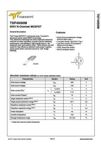
TSF4N90M 900V N-Channel MOSFET General Description Features This Power MOSFET is produced using Truesemi s Drain-Source breakdown voltage advanced planar stripe DMOS technology. BVDSS=900V (Min.) This advanced technology has been especially tailored to minimize on-state resistance, provide superior switching Low gate charge Qg=22nC (Typ.) performance, and withstand high
wml4n90d1 wmk4n90d1 wmm4n90d1.pdf
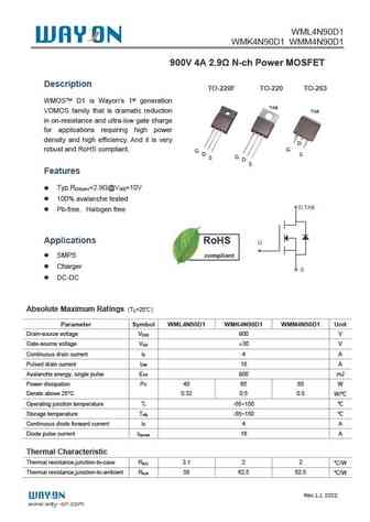
WML4N90D1 WMK4N90D1 WMM4N90D1 900V 4A 2.9 N-ch Power MOSFET Description TO-220F TO-220 TO-263 WMOSTM D1 is Wayon s 1st generation TAB VDMOS family that is dramatic reduction TAB in on-resistance and ultra-low gate charge for applications requiring high power density and high efficiency. And it is very D G robust and RoHS compliant. G D S G S D S Features Typ.R =2.9
wmk4n90d1b wml4n90d1b wmm4n90d1b.pdf
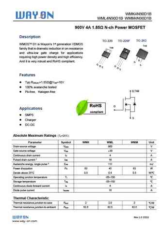
WMK4N90D1B WML4N90D1B WMM4N90D1B 900V 4A 1.85 N-ch Power MOSFET Description TO-263 TO-220 TO-220F WMOSTM D1 is Wayon s 1st generation VDMOS TAB TAB family that is dramatic reduction in on-resistance and ultra-low gate charge for applications requiring high power density and high efficiency. D And it is very robust and RoHS compliant. G G S D S G D S
cs4n90f cs4n90p.pdf
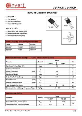
nvert Suzhou Convert Semiconductor Co ., Ltd. CS4N90F, CS4N90P 900V N-Channel MOSFET FEATURES Fast switching 100% avalanche tested Improved dv/dt capability APPLICATIONS Switch Mode Power Supply (SMPS) Uninterruptible Power Supply (UPS) Power Factor Correction (PFC) Device Marking and Package Information Device Package Marking CS4N90F TO-220F CS4N90F CS4N9
fir4n90fg.pdf
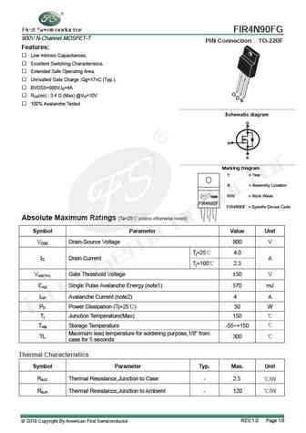
FIR4N90FG 900V N-Channel MOSFET-T PIN Connection TO-220F Features Low Intrinsic Capacitances. Excellent Switching Characteristics. Extended Safe Operating Area. Unrivalled Gate Charge Qg=17nC (Typ.). BVDSS=900V,ID=4A G RDS(on) 3.4 (Max) @VG=10V D S 100% Avalanche Tested g Schematic dia ram D G S Marking Diagram Y = Year A = Assembl
hm4n90i.pdf
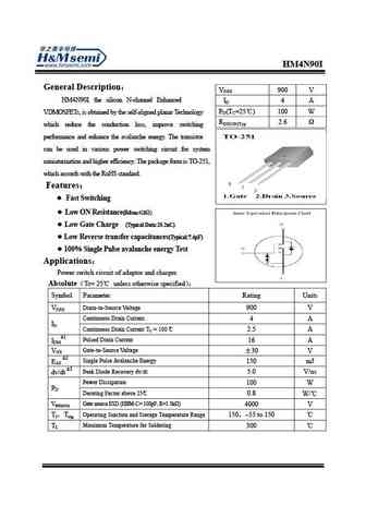
HM4N90I General Description VDSS 900 V HM4N90I, the silicon N-channel Enhanced ID 4 A PD(TC=25 ) 100 W VDMOSFETs, is obtained by the self-aligned planar Technology RDS(ON)Typ 2.6 which reduce the conduction loss, improve switching performance and enhance the avalanche energy. The transistor can be used in various power switching circuit for system miniaturization
aotf4n90.pdf
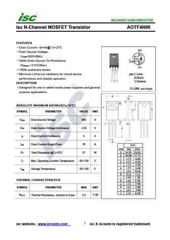
isc N-Channel MOSFET Transistor AOTF4N90 FEATURES Drain Current I =4A@ T =25 D C Drain Source Voltage- V =900V(Min) DSS Static Drain-Source On-Resistance R =3.6 (Max) DS(on) 100% avalanche tested Minimum Lot-to-Lot variations for robust device performance and reliable operation DESCRIPTION Designed for use in switch mode power supplies and general purpose a
Otros transistores... 10N90 , 11N90 , 12N90 , 9N95 , 9N100 , 1N90 , 2N90 , 3N90 , IRFB4115 , 5N90 , 6N90 , 7N90 , 1N80 , 2N80 , 3N80 , 4N80 , 5N80 .
🌐 : EN ES РУ

Liste
Recientemente añadidas las descripciónes de los transistores:
MOSFET: ASU70R600E | ASU65R850E | ASU65R550E | ASU65R350E | ASR65R120EFD | ASR65R046EFD | ASQ65R046EFD | ASM65R280E | ASM60R330E | ASE70R950E | ASD80R750E | ASD70R950E | ASD70R600E | ASD70R380E | ASD65R850E | ASD65R550E
Popular searches
irlz24n | irf620 | irfp350 | 13003 transistor | c458 transistor | 2sc1775 | 2n1305 | 2sc5242