6N90 MOSFET Equivalente. Reemplazo. Hoja de especificaciones. Principales características
Número de Parte: 6N90
Tipo de FET: MOSFET
Polaridad de transistor: N
ESPECIFICACIONES MÁXIMAS
Pdⓘ - Máxima disipación de potencia: 167 W
|Vds|ⓘ - Voltaje máximo drenador-fuente: 900 V
|Vgs|ⓘ - Voltaje máximo fuente-puerta: 30 V
|Id|ⓘ - Corriente continua de drenaje: 6.2 A
Tjⓘ - Temperatura máxima de unión: 150 °C
CARACTERÍSTICAS ELÉCTRICAS
trⓘ - Tiempo de subida: 90 nS
Cossⓘ - Capacitancia de salida: 110 pF
RDSonⓘ - Resistencia estado encendido drenaje a fuente: 1.85 Ohm
Encapsulados: TO-220F1 TO-220 TO-262
Búsqueda de reemplazo de 6N90 MOSFET
- Selecciónⓘ de transistores por parámetros
6N90 datasheet
6n90.pdf
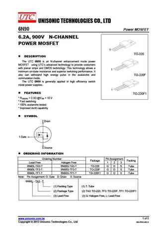
UNISONIC TECHNOLOGIES CO., LTD 6N90 Power MOSFET 6.2A, 900V N-CHANNEL POWER MOSFET 1 TO-220 DESCRIPTION The UTC 6N90 is an N-channel enhancement mode power MOSFET using UTC s advanced technology to provide costumers with planar stripe and DMOS technology. This technology allows a 1 minimum on-state resistance and superior switching performance. It also can withstand h
stf6n90k5.pdf
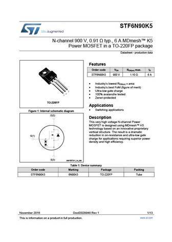
STF6N90K5 N-channel 900 V, 0.91 typ., 6 A MDmesh K5 Power MOSFET in a TO-220FP package Datasheet - production data Features Order code V R max. I DS DS(on) D STF6N90K5 900 V 1.10 6 A Industry s lowest R x area DS(on) Industry s best FoM (figure of merit) Ultra-low gate charge 100% avalanche tested Zener-protected TO-220FP Applications
stp6n90k5.pdf
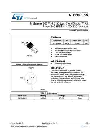
STP6N90K5 N-channel 900 V, 0.91 typ., 6 A MDmesh K5 Power MOSFET in a TO-220 package Datasheet - production data Features Order code V R max. I DS DS(on) D TAB STP6N90K5 900 V 1.10 6 A Industry s lowest R x area DS(on) Industry s best FoM (figure of merit) 3 2 Ultra-low gate charge 1 100% avalanche tested TO-220 Zener-protected App
fqpf6n90ct.pdf

TM QFET FQP6N90C/FQPF6N90C 900V N-Channel MOSFET General Description Features These N-Channel enhancement mode power field effect 6A, 900V, RDS(on) = 2.3 @VGS = 10 V transistors are produced using Fairchild s proprietary, Low gate charge ( typical 30 nC) planar stripe, DMOS technology. Low Crss ( typical 11 pF) This advanced technology has been especially tailored to
fqb6n90tm am002.pdf
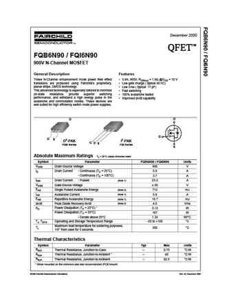
December 2000 TM QFET QFET QFET QFET FQB6N90 / FQI6N90 900V N-Channel MOSFET General Description Features These N-Channel enhancement mode power field effect 5.8A, 900V, RDS(on) = 1.9 @VGS = 10 V transistors are produced using Fairchild s proprietary, Low gate charge ( typical 40 nC) planar stripe, DMOS technology. Low Crss ( typical 17 pF) This advanced technology
fqp6n90c fqpf6n90c.pdf
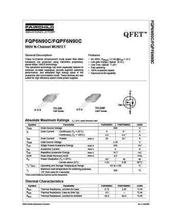
TM QFET FQP6N90C/FQPF6N90C 900V N-Channel MOSFET General Description Features These N-Channel enhancement mode power field effect 6A, 900V, RDS(on) = 2.3 @VGS = 10 V transistors are produced using Fairchild s proprietary, Low gate charge ( typical 30 nC) planar stripe, DMOS technology. Low Crss ( typical 11 pF) This advanced technology has been especially tailored to
fqpf6n90.pdf
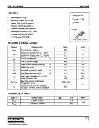
QFET N-CHANNEL FQPF6N90 FEATURES BVDSS = 900V Advanced New Design RDS(ON) = 1.9 Avalanche Rugged Technology ID = 3.4A Rugged Gate Oxide Technology Very Low Intrinsic Capacitances Excellent Switching Characteristics TO-220F Unrivalled Gate Charge 40nC (Typ.) Extended Safe Operating Area Lower RDS(ON) 1.5 (Typ.) 1 2 3 1. Gate 2. Drain 3. Sou
fqp6n90.pdf
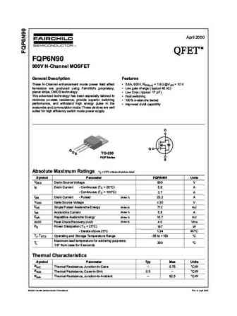
April 2000 TM QFET QFET QFET QFET 900V N-ChanneI MOSFET GeneraI Description Features These N-Channel enhancement mode power field effect 5.8A, 900V, RDS(on) = 1.9 @VGS = 10 V transistors are produced using Fairchild s proprietary, Low gate charge ( typical 40 nC) planar stripe, DMOS technology. Low Crss ( typical 17 pF) This advanced technology has been es
fqa6n90.pdf
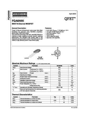
April 2000 TM QFET QFET QFET QFET 900V N-ChanneI MOSFET GeneraI Description Features These N-Channel enhancement mode power field effect 6.4A, 900V, RDS(on) = 1.9 @VGS = 10 V transistors are produced using Fairchild s proprietary, Low gate charge ( typical 40 nC) planar stripe, DMOS technology. Low Crss ( typical 17 pF) This advanced technology has been es
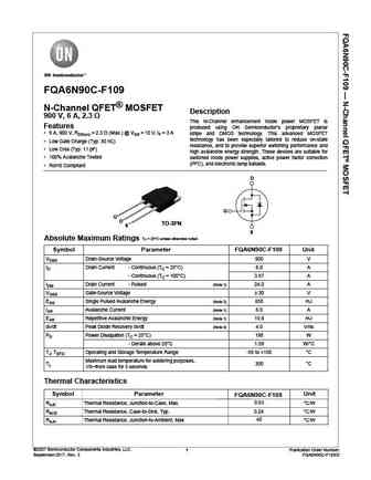
fqa6n90c f109.pdf
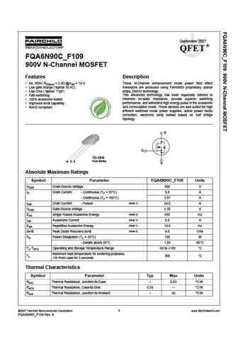
September 2007 QFET FQA6N90C_F109 900V N-Channel MOSFET Features Description 6A, 900V, RDS(on) = 2.3 @VGS = 10 V These N-Channel enhancement mode power field effect Low gate charge ( typical 30 nC) transistors are produced using Fairchild s proprietary, planar stripe, DMOS technology. Low Crss ( typical 11pF) This advanced technology has been especially tailored t
fqaf6n90.pdf
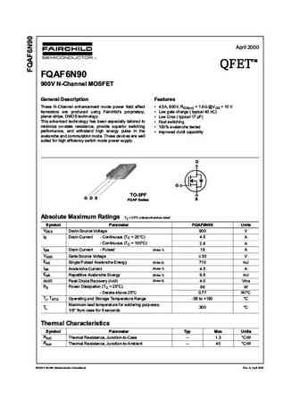
April 2000 TM QFET QFET QFET QFET 900V N-ChanneI MOSFET GeneraI Description Features These N-Channel enhancement mode power field effect 4.5A, 900V, RDS(on) = 1.9 @VGS = 10 V transistors are produced using Fairchild s proprietary, Low gate charge ( typical 40 nC) planar stripe, DMOS technology. Low Crss ( typical 17 pF) This advanced technology has been es
ssh6n90a.pdf
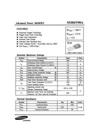
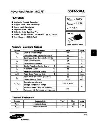
Advanced Power MOSFET FEATURES BVDSS = 900 V Avalanche Rugged Technology RDS(on) = 2.3 Rugged Gate Oxide Technology Lower Input Capacitance ID = 6 A Improved Gate Charge Extended Safe Operating Area Lower Leakage Current 25 A (Max.) @ VDS = 900V Low RDS(ON) 1.829 (Typ.) 1 2 3 1.Gate 2. Drain 3. Source Absolute Maximum Ratings Symbol Characteristic Value
sss6n90a.pdf
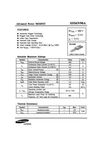
Advanced Power MOSFET FEATURES BVDSS = 900 V Avalanche Rugged Technology RDS(on) = 2.3 Rugged Gate Oxide Technology Lower Input Capacitance ID = 3.5 A Improved Gate Charge Extended Safe Operating Area Lower Leakage Current 25 A (Max.) @ VDS = 900V Low RDS(ON) 1.829 (Typ.) 1 2 3 1.Gate 2. Drain 3. Source Absolute Maximum Ratings Symbol Characteristic Value
ssp6n90a.pdf
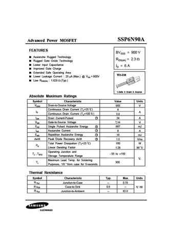
Advanced Power MOSFET FEATURES BVDSS = 900 V Avalanche Rugged Technology RDS(on) = 2.3 Rugged Gate Oxide Technology Lower Input Capacitance ID = 6 A Improved Gate Charge Extended Safe Operating Area Lower Leakage Current 25 A (Max.) @ VDS = 900V Low RDS(ON) 1.829 (Typ.) 1 2 3 1.Gate 2. Drain 3. Source Absolute Maximum Ratings Symbol Characteristic Value
ixfk26n90 ixfx26n90 ixfk25n90 ixfx25n90.pdf
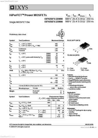
www.DataSheet4U.com VDSS IDSS RDS(on) trr HiPerFETTM Power MOSFETs IXFK/IXFX 26N90 900 V 26 A 0.30 W 250 ns IXFK/IXFX 25N90 900 V 25 A 0.33 W 250 ns Single MOSFET Die Preliminary data sheet Symbol Test Conditions Maximum Ratings PLUS 247TM (IXFX) VDSS TJ = 25 C to 150 C 900 V VDGR TJ = 25 C to 150 C; RGS = 1 MW 900 V VGS Continuous 20 V (TAB) G VGSM Transient 30 V D S ID2
ixfh16n90 ixfx16n90.pdf
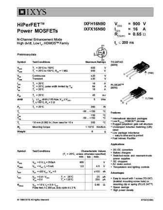
IXFH16N90 VDSS = 900 V HiPerFETTM IXFX16N90 ID25 = 16 A Power MOSFETs RDS(on) = 0.65 W N-Channel Enhancement Mode t 200 ns High dv/dt, Low t , HDMOSTM Family rr rr Preliminary data Symbol Test Conditions Maximum Ratings TO-247 AD (IXFH) VDSS TJ = 25 C to 150 C 900 V VDGR TJ = 25 C to 150 C; RGS = 1 M 900 V (TAB) VGS Continuous 20 V VGSM Transient 30 V ID25 TC = 2
ixfn26n90 ixfn25n90.pdf
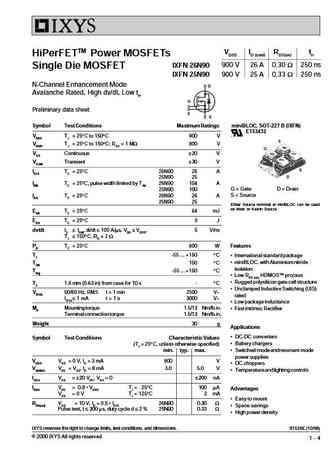
VDSS ID (cont) RDS(on) trr HiPerFETTM Power MOSFETs 900 V 26 A 0.30 W 250 ns IXFN 26N90 Single Die MOSFET IXFN 25N90 900 V 25 A 0.33 W 250 ns N-Channel Enhancement Mode D Avalanche Rated, High dv/dt, Low trr G Preliminary data sheet S S Symbol Test Conditions Maximum Ratings miniBLOC, SOT-227 B (IXFN) E153432 VDSS TJ = 25 C to 150 C 900 V S VDGR TJ = 25 C to 150 C; RGS =
ixth6n90-a ixtm6n90-a.pdf
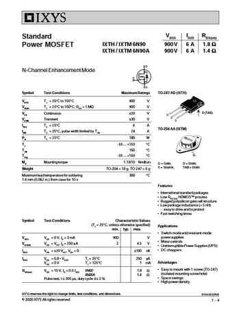
VDSS ID25 RDS(on) Standard IXTH / IXTM 6N90 900 V 6 A 1.8 Power MOSFET IXTH / IXTM 6N90A 900 V 6 A 1.4 N-Channel Enhancement Mode Symbol Test Conditions Maximum Ratings TO-247 AD (IXTH) VDSS TJ = 25 C to 150 C 900 V VDGR TJ = 25 C to 150 C; RGS = 1 M 900 V D (TAB) VGS Continuous 20 V VGSM Transient 30 V ID25 TC = 25 C6 A T
ixfh6n90 ixfh6n100 ixfm6n90 ixfm6n100.pdf
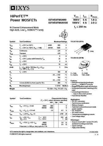
VDSS ID25 RDS(on) HiPerFETTM IXFH/IXFM 6 N90 900 V 6 A 1.8 W Power MOSFETs IXFH/IXFM 6 N100 1000 V 6 A 2.0 W trr 250 ns N-Channel Enhancement Mode High dv/dt, Low trr, HDMOSTM Family Symbol Test Conditions Maximum Ratings TO-247 AD (IXFH) VDSS TJ = 25 C to 150 C 6N90 900 V VDGR TJ = 25 C to 150 C; RGS = 1 MW 6N100 1000 V VGS Continuous 20 V (TAB) VGSM Transient 30 V ID2
fqa6n90c-f109.pdf
FQA6N90C-F109 N-Channel QFET MOSFET Description 900 V, 6 A, 2.3 This N-Channel enhancement mode power MOSFET is Features produced using ON Semiconductor s proprietary planar 6 A, 900 V, RDS(on) = 2.3 (Max.) @ VGS = 10 V, ID = 3 A stripe and DMOS technology. This advanced MOSFET technology has been especially tailored to reduce on-state Low Gate Charge (Typ. 3
fqp6n90c fqpf6n90c.pdf

Is Now Part of To learn more about ON Semiconductor, please visit our website at www.onsemi.com Please note As part of the Fairchild Semiconductor integration, some of the Fairchild orderable part numbers will need to change in order to meet ON Semiconductor s system requirements. Since the ON Semiconductor product management systems do not have the ability to manage part nomenclatur
fmh06n90e.pdf
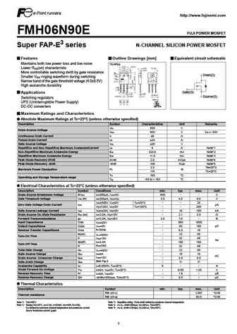
http //www.fujisemi.com FMH06N90E FUJI POWER MOSFET Super FAP-E3 series N-CHANNEL SILICON POWER MOSFET Features Outline Drawings [mm] Equivalent circuit schematic Maintains both low power loss and low noise TO-3P(Q) Lower R (on) characteristic DS More controllable switching dv/dt by gate resistance Drain(D) Smaller V ringing waveform during switching GS Narrow band of the gate thres
fmv06n90e.pdf
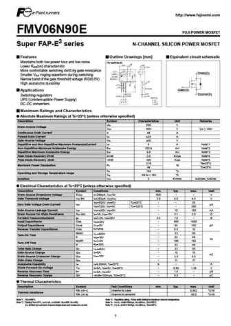
http //www.fujisemi.com FMV06N90E FUJI POWER MOSFET Super FAP-E3 series N-CHANNEL SILICON POWER MOSFET Features Outline Drawings [mm] Equivalent circuit schematic Maintains both low power loss and low noise TO-220F(SLS) Lower R (on) characteristic DS More controllable switching dv/dt by gate resistance Drain(D) Smaller V ringing waveform during switching GS Narrow band of the gate t
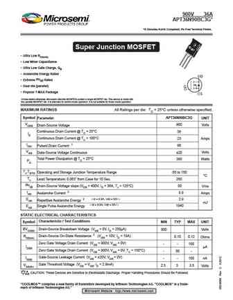
apt36n90bc3g.pdf
900V 36A APT36N90BC3G* *G Denotes RoHS Compliant, Pb Free Terminal Finish. Super Junction MOSFET D3 Ultra Low RDS(ON) Low Miller Capacitance Ultra Low Gate Charge, Qg Avalanche Energy Rated D Extreme dv/dt Rated Dual die (parallel) G Popular T-MAX Package S Unless stated otherwise, Microsemi discrete MOSFETs contain a single MOSFET die. This de
aotf6n90.pdf
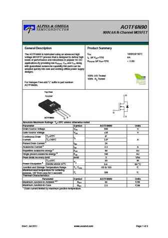
AOTF6N90 900V,6A N-Channel MOSFET General Description Product Summary VDS 1000V@150 The AOTF6N90 is fabricated using an advanced high voltage MOSFET process that is designed to deliver high ID (at VGS=10V) 6A levels of performance and robustness in popular AC-DC RDS(ON) (at VGS=10V)
jcs6n90fa jcs6n90ba jcs6n90sa jcs6n90ca jcs6n90gda.pdf
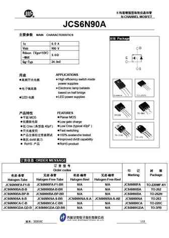
N R N-CHANNEL MOSFET JCS6N90A MAIN CHARACTERISTICS Package ID 6.0 A VDSS 900 V Rdson Vgs=10V 3.0 -MAX Qg-Typ 24.0nC APPLICATIONS High efficiency switch mode . power supplies Electronic lamp ballasts based on half bridge LED power suppli
jcs6n90ch jcs6n90fh jcs6n90b.pdf
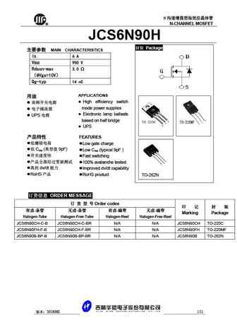
N R N-CHANNEL MOSFET JCS6N90H Package MAIN CHARACTERISTICS ID 6 A VDSS 900 V Rdson-max 3.0 @Vgs=10V Qg-typ 14 nC APPLICATIONS High efficiency switch mode power supplies Electronic lamp ballasts UPS based on half bridge UP
6n90a 6n90af.pdf
RoHS 6N90 Series RoHS SEMICONDUCTOR Nell High Power Products N-Channel Power MOSFET 6A, 900Volts DESCRIPTION D The Nell 6N90 is a three-terminal silicon device with current conduction capability of 6A, fast switching speed, low on-state resistance, breakdown voltage rating of 900V, and max. threshold voltage of 5 volts. They are designed for use in applications such as G DS G
cs6n90f a9h.pdf
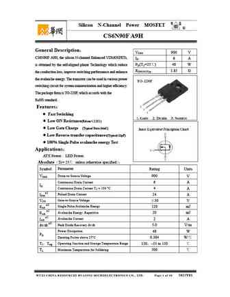
Silicon N-Channel Power MOSFET R CS6N90F A9H General Description VDSS 900 V CS6N90F A9H, the silicon N-channel Enhanced VDMOSFETs, ID 6 A PD(TC=25 ) 48 W is obtained by the self-aligned planar Technology which reduce RDS(ON)Typ 1.85 the conduction loss, improve switching performance and enhance the avalanche energy. The transistor can be used in various powe
cs6n90 a8h.pdf
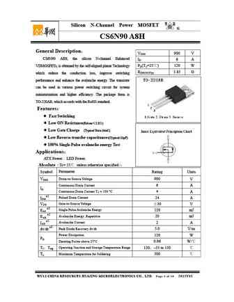
Silicon N-Channel Power MOSFET R CS6N90 A8H General Description VDSS 900 V CS6N90 A8H, the silicon N-channel Enhanced ID 6 A PD(TC=25 ) 120 W VDMOSFETs, is obtained by the self-aligned planar Technology RDS(ON)Typ 1.85 which reduce the conduction loss, improve switching performance and enhance the avalanche energy. The transistor can be used in various power
cs6n90 arh-g.pdf

Silicon N-Channel Power MOSFET R CS6N90 ARH-G General Description VDSS 900 V CS6N90 ARH-G, the silicon N-channel Enhanced ID 6 A PD(TC=25 ) 48 W VDMOSFETs, is obtained by the self-aligned planar Technology RDS(ON)Typ 1.85 which reduce the conduction loss, improve switching performance and enhance the avalanche energy. The transistor can be used in various
f6n90.pdf
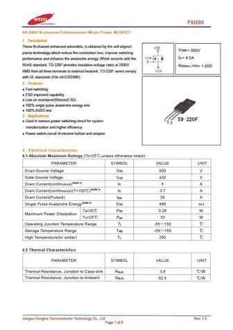
F6N90 6A 900V N-channel Enhancement Mode Power MOSFET 1 Description These N-channel enhanced vdmosfets, is obtained by the self-aligned V DSS = 900V planar technology which reduce the conduction loss, improve switching I = 6.0A D performance and enhance the avalanche energy. Which accords with the RoHS standard. TO-220F provides insulation voltage rated at 2000V R DS(on) TYP) = 1
msf6n90.pdf

MSF6N90 900V N-Channel MOSFET Description The MS15N50 is a N-channel enhancement-mode MOSFET, providing the designer with the best combination of fast switching, ruggedized device design, low on-resistance and cost effectiveness. The ITO-220 package is universally preferred for all commercial-industrial applications Features RDS(on) (Max 2.4 )@VGS=10V Gate Charg
ms6n90.pdf

MS6N90 900V N-Channel MOSFET Description The MS6N90 is a N-channel enhancement-mode MOSFET, providing the designer with the best combination of fast switching, ruggedized device design, low on-resistance and cost effectiveness. The TO-220 package is universally preferred for all commercial-industrial applications Features RDS(on) (Max 2.4 )@VGS=10V Gate Charge (
fhp6n90a fhf6n90a.pdf
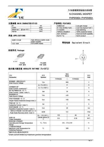
N N-CHANNEL MOSFET FHP6N90A /FHF6N90A MAIN CHARACTERISTICS FEATURES ID 6A Low gate charge VDSS 900V Crss ( 11pF) Low Crss (typical 11pF ) Rdson-typ @Vgs=10V 1.5 Fast switching Qg-typ 34nC 100% 100% avalanche tested dv/dt Improv
swf6n90d swj6n90d.pdf
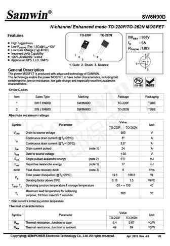
SW6N90D N-channel Enhanced mode TO-220F/TO-262N MOSFET TO-220F TO-262N Features BVDSS 900V ID 6A High ruggedness Low RDS(ON) (Typ 1.8 )@VGS=10V RDS(ON) 1.8 Low Gate Charge (Typ 42nC) Improved dv/dt Capability 2 1 1 100% Avalanche Tested 2 2 3 3 Application UPS, LED, SMPS 1 1. Gate 2. Drain 3. Source 3 General Description
hfh6n90.pdf
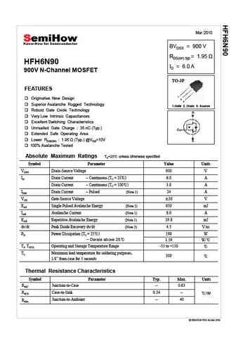
Mar 2010 BVDSS = 900 V RDS(on) typ HFH6N90 ID = 6.0 A 900V N-Channel MOSFET TO-3P FEATURES 1 Originative New Design 2 3 Superior Avalanche Rugged Technology 1.Gate 2. Drain 3. Source Robust Gate Oxide Technology Very Low Intrinsic Capacitances Excellent Switching Characteristics Unrivalled Gate Charge 35 nC (Typ.) Extended Safe Operating Area Lower RDS(ON
hfs6n90.pdf
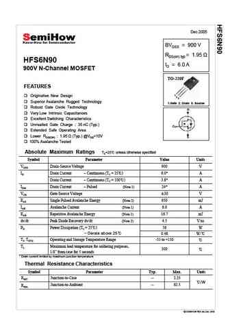
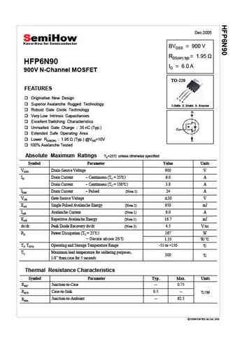
Dec 2005 BVDSS = 900 V RDS(on) typ HFS6N90 ID = 6.0 A 900V N-Channel MOSFET TO-220F FEATURES 1 Originative New Design 2 3 Superior Avalanche Rugged Technology 1.Gate 2. Drain 3. Source Robust Gate Oxide Technology Very Low Intrinsic Capacitances Excellent Switching Characteristics Unrivalled Gate Charge 35 nC (Typ.) Extended Safe Operating Area Lower RDS(
hfw6n90.pdf
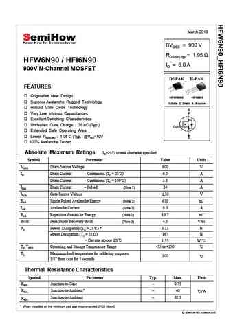
March 2013 BVDSS = 900 V RDS(on) typ = 1.95 HFW6N90 / HFI6N90 ID = 6.0 A 900V N-Channel MOSFET D2-PAK I2-PAK FEATURES Originative New Design HFW6N90 HFI6N90 Superior Avalanche Rugged Technology 1.Gate 2. Drain 3. Source Robust Gate Oxide Technology Very Low Intrinsic Capacitances Excellent Switching Characteristics Unrivalled Gate Charge 35 nC (Typ.) Extended
hfp6n90.pdf
Dec 2005 BVDSS = 900 V RDS(on) typ HFP6N90 ID = 6.0 A 900V N-Channel MOSFET TO-220 FEATURES Originative New Design 1 2 3 Superior Avalanche Rugged Technology 1.Gate 2. Drain 3. Source Robust Gate Oxide Technology Very Low Intrinsic Capacitances Excellent Switching Characteristics Unrivalled Gate Charge 35 nC (Typ.) Extended Safe Operating Area Lower RDS(ON
mtm6n90.pdf
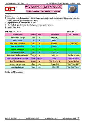
Shaanxi Qunli Electric Co., Ltd Add. No. 1 Qunli Road,Baoji City,Shaanxi,China WVM6N90(MTM6N90) Power MOSFET(N-channel) Transistor Features 1. It s voltage control component with good input impedance, small starting power dissipation, wide area of safe operation, good temperature stability. 2. Implementation of standards QZJ840611 3. Use for high speed switch, circuit of power
wmk6n90d1 wml6n90d1 wmm6n90d1.pdf
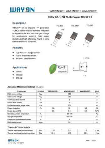
WMK6N90D1 WML6N90D1 WMM6N90D1 900V 6A 1.7 N-ch Power MOSFET Description TO-263 TO-220 TO-220F WMOSTM D1 is Wayon s 1st generation TAB VDMOS family that is dramatic reduction in on-resistance and ultra-low gate charge for applications requiring high power density and high efficiency. And it is very robust and RoHS compliant. D G G G D D S S S Features Typ.R =1.7 @V =
cs6n90arh-g.pdf
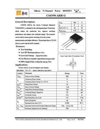
Silicon N-Channel Power MOSFET R CS6N90 ARH-G General Description VDSS 900 V CS6N90 ARH-G, the silicon N-channel Enhanced ID 6 A PD(TC=25 ) 48 W VDMOSFETs, is obtained by the self-aligned planar Technology RDS(ON)Typ 1.85 which reduce the conduction loss, improve switching performance and enhance the avalanche energy. The transistor can be used in various
cs6n90f cs6n90p cs6n90b.pdf
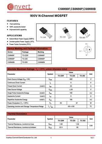
nvert Suzhou Convert Semiconductor Co ., Ltd. CS6N90F,CS6N90P,CS6N90B 900V N-Channel MOSFET FEATURES Fast switching 100% avalanche tested Improved dv/dt capability APPLICATIONS Switch Mode Power Supply (SMPS) Uninterruptible Power Supply (UPS) Power Factor Correction (PFC) Device Marking and Package Information Device Package Marking CS6N90F TO-220F CS6N90F
cs6n90f cs6n90p cs6n90b cs6n90w.pdf
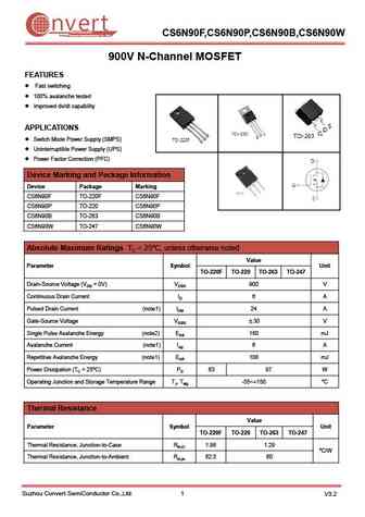
nvert Suzhou Convert Semiconductor Co ., Ltd. CS6N90F,CS6N90P,CS6N90B,CS6N90W 900V N-Channel MOSFET FEATURES Fast switching 100% avalanche tested Improved dv/dt capability APPLICATIONS Switch Mode Power Supply (SMPS) Uninterruptible Power Supply (UPS) Power Factor Correction (PFC) Device Marking and Package Information Device Package Marking CS6N90F TO-220F
fir6n90fg.pdf
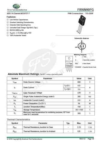
FIR6N90FG 900V N-Channel MOSFET-T PIN Connection TO-220F Features Low Intrinsic Capacitances. Excellent Switching Characteristics. Extended Safe Operating Area. Unrivalled Gate Charge Qg=30nC (Typ.). BVDSS=900V,ID=6A G D S RDS(on) 2.1 (Max) @VG=10V 100% Avalanche Tested g Schematic dia ram D G S Marking Diagram Y = Year A = Assembly L
tma6n90h tmp6n90h.pdf
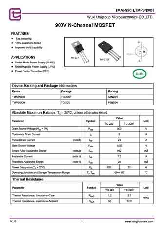
TMA6N90H,TMP6N90H Wuxi Unigroup Microelectronics CO.,LTD. 900V N-Channel MOSFET FEATURES Fast switching 100% avalanche tested Improved dv/dt capability APPLICATIONS Switch Mode Power Supply (SMPS) Uninterruptible Power Supply (UPS) Power Factor Correction (PFC) Device Marking and Package Information Device Package Marking TMA6N90H TO-220F A6N90
hm6n90.pdf
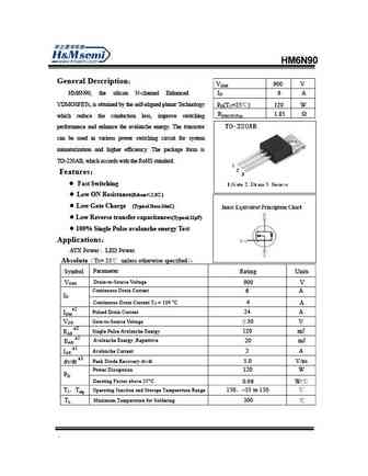
HM6N90 General Description VDSS 900 V HM6N90, the silicon N-channel Enhanced ID 6 A VDMOSFETs, is obtained by the self-aligned planar Technology PD(TC=25 ) 120 W RDS(ON)Typ 1.85 which reduce the conduction loss, improve switching performance and enhance the avalanche energy. The transistor can be used in various power switching circuit for system miniaturization and
sfp049n90c3 sfb046n90c3.pdf

SFP049N90C3,SFB046N90C3 N-MOSFET 90V, 3.9m , 120A Features Product Summary Extremely low on-resistance RDS(on) VDS 90V Excellent QgxRDS(on) product(FOM) RDS(on) 3.9m Qualified according to JEDEC criteria ID 120A 100% DVDS Tested Applications 100% Avalanche Tested Motor control and drive Battery management UPS (Uninterrupible Power Supplies) SFP049N90
aotf6n90.pdf
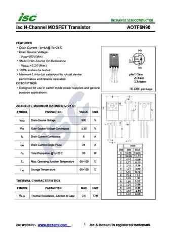
isc N-Channel MOSFET Transistor AOTF6N90 FEATURES Drain Current I =6A@ T =25 D C Drain Source Voltage- V =900V(Min) DSS Static Drain-Source On-Resistance R =2.2 (Max) DS(on) 100% avalanche tested Minimum Lot-to-Lot variations for robust device performance and reliable operation DESCRIPTION Designed for use in switch mode power supplies and general purpose a
stf6n90k5.pdf
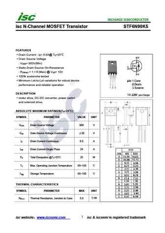
isc N-Channel MOSFET Transistor STF6N90K5 FEATURES Drain Current I = 6.0A@ T =25 D C Drain Source Voltage V = 900V(Min) DSS Static Drain-Source On-Resistance R = 1.1 (Max) @ V = 10V DS(on) GS 100% avalanche tested Minimum Lot-to-Lot variations for robust device performance and reliable operation DESCRIPTION motor drive, DC-DC converter, power switch and sole
Otros transistores... 12N90 , 9N95 , 9N100 , 1N90 , 2N90 , 3N90 , 4N90 , 5N90 , P55NF06 , 7N90 , 1N80 , 2N80 , 3N80 , 4N80 , 5N80 , 6N80 , 7N80 .
History: IXFK26N90
History: IXFK26N90
🌐 : EN ES РУ

Liste
Recientemente añadidas las descripciónes de los transistores:
MOSFET: ASU70R600E | ASU65R850E | ASU65R550E | ASU65R350E | ASR65R120EFD | ASR65R046EFD | ASQ65R046EFD | ASM65R280E | ASM60R330E | ASE70R950E | ASD80R750E | ASD70R950E | ASD70R600E | ASD70R380E | ASD65R850E | ASD65R550E
Popular searches
irfp350 | 13003 transistor | c458 transistor | 2sc1775 | 2n1305 | 2sc5242 | irf540 equivalent | mp1620 transistor equivalent