7N70 MOSFET Equivalente. Reemplazo. Hoja de especificaciones. Principales características
Número de Parte: 7N70
Tipo de FET: MOSFET
Polaridad de transistor: N
ESPECIFICACIONES MÁXIMAS
Pdⓘ - Máxima
disipación de potencia: 142 W
|Vds|ⓘ - Voltaje máximo drenador-fuente: 700 V
|Vgs|ⓘ - Voltaje máximo fuente-puerta: 30 V
|Id|ⓘ - Corriente continua
de drenaje: 7 A
Tjⓘ - Temperatura máxima de unión: 150 °C
CARACTERÍSTICAS ELÉCTRICAS
trⓘ - Tiempo
de subida: 79 nS
Cossⓘ - Capacitancia de salida: 150 pF
RDSonⓘ - Resistencia estado encendido drenaje a fuente: 1.4 Ohm
Encapsulados: TO-263
TO-220
TO-220F
Búsqueda de reemplazo de 7N70 MOSFET
- Selecciónⓘ de transistores por parámetros
7N70 datasheet
..1. Size:393K utc
7n70.pdf 
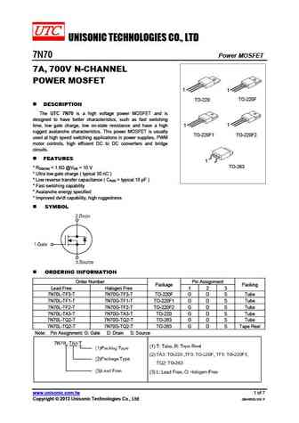
UNISONIC TECHNOLOGIES CO., LTD 7N70 Power MOSFET 7A, 700V N-CHANNEL POWER MOSFET 1 1 TO-220 TO-220F DESCRIPTION The UTC 7N70 is a high voltage power MOSFET and is designed to have better characteristics, such as fast switching 1 time, low gate charge, low on-state resistance and have a high 1 rugged avalanche characteristics. This power MOSFET is usually TO-220F1 TO-2
0.1. Size:278K diodes
dmj7n70sk3.pdf
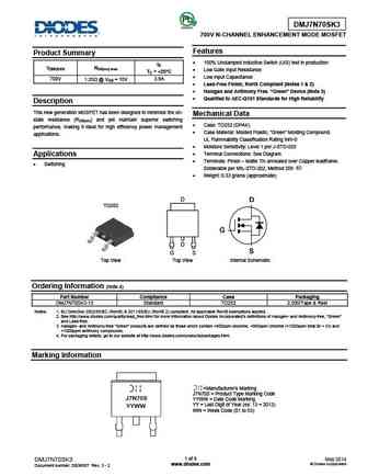
DMJ7N70SK3 700V N-CHANNEL ENHANCEMENT MODE MOSFET Features Product Summary 100% Unclamped Inductive Switch (UIS) test in production ID V(BR)DSS RDS(on) max Low Gate Input Resistance TC = +25 C Low Input Capacitance 700V 1.25 @ VGS = 10V 3.9A Lead-Free Finish; RoHS Compliant (Notes 1 & 2) Halogen and Antimony Free. Green Device (Note 3)
0.2. Size:945K infineon
ss07n70.pdf
MOSFET Metal Oxide Semiconductor Field Effect Transistor CoolMOS C6 700V 700V CoolMOS C6 Power Transistor SS07N70 Data Sheet ev. 0 in l Industrial & Multimarket 700V CoolMOS C6 Power Transistor SS07N70 IPAK SL 1 Descripti n t b CoolMOS is a revolutionary technology for high voltage power MOSFETs designed according to the superjunction (S ) principle and pioneered by Infineon
0.3. Size:208K utc
7n70l-tf1-t 7n70g-tf1-t.pdf
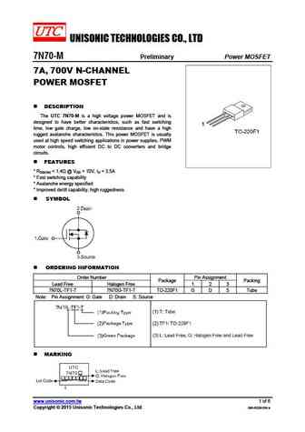
UNISONIC TECHNOLOGIES CO., LTD 7N70-M Preliminary Power MOSFET 7A, 700V N-CHANNEL POWER MOSFET DESCRIPTION The UTC 7N70-M is a high voltage power MOSFET and is designed to have better characteristics, such as fast switching time, low gate charge, low on-state resistance and have a high rugged avalanche characteristics. This power MOSFET is usually used at high speed switch
0.4. Size:540K aosemi
aotf7n70.pdf

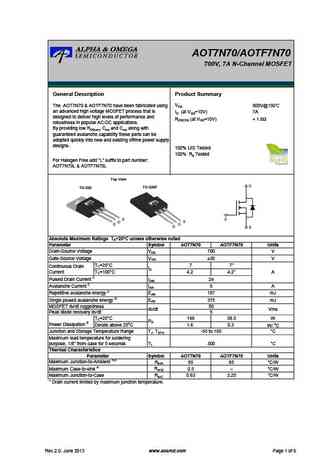
AOT7N70/AOTF7N70 700V, 7A N-Channel MOSFET General Description Product Summary VDS 800V@150 The AOT7N70 & AOTF7N70 have been fabricated using an advanced high voltage MOSFET process that is ID (at VGS=10V) 7A designed to deliver high levels of performance and RDS(ON) (at VGS=10V)
0.5. Size:540K aosemi
aot7n70.pdf
AOT7N70/AOTF7N70 700V, 7A N-Channel MOSFET General Description Product Summary VDS 800V@150 The AOT7N70 & AOTF7N70 have been fabricated using an advanced high voltage MOSFET process that is ID (at VGS=10V) 7A designed to deliver high levels of performance and RDS(ON) (at VGS=10V)
0.6. Size:376K aosemi
aot7n70 aotf7n70.pdf
AOT7N70/AOTF7N70 700V, 7A N-Channel MOSFET General Description Product Summary VDS 800V@150 The AOT7N70 & AOTF7N70 have been fabricated using an advanced high voltage MOSFET process that is ID (at VGS=10V) 7A designed to deliver high levels of performance and RDS(ON) (at VGS=10V)
0.7. Size:98K ape
ap07n70ci-h.pdf
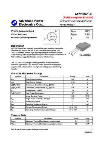
AP07N70CI-H RoHS-compliant Product Advanced Power N-CHANNEL ENHANCEMENT MODE Electronics Corp. POWER MOSFET 100% Avalanche Rated BVDSS 700V D Fast Switching RDS(ON) 1.4 Simple Drive Requirement ID 7A G S Description AP07N70 series are specially designed as main switching devices for universal 90 265VAC off-line AC/DC converter applications. The TO-220CFM type provide
0.8. Size:361K sisemi
sif7n70c.pdf
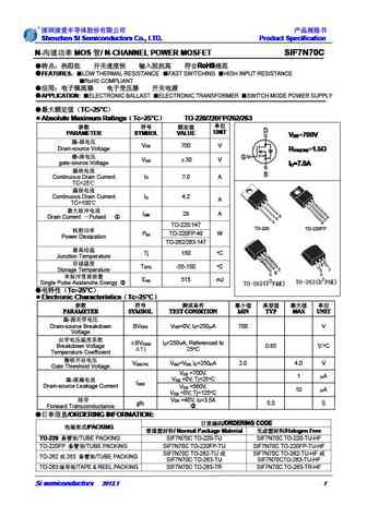
Shenzhen SI Semiconductors Co., LTD. Product Specification Shenzhen SI Semiconductors Co., LTD. Product Specification Shenzhen SI Semiconductors Co., LTD. Product Specification Shenzhen SI Semiconductors Co., LTD. Product Specification N- MOS / N-CHANNEL POWER MOSFET SIF7N70C N- MOS / N-CHANNEL POWER MOSFET SIF7N70C N
0.9. Size:1944K jilin sino
jcs7n70v jcs7n70r jcs7n70c jcs7n70f jcs7n70s jcs7n70b.pdf
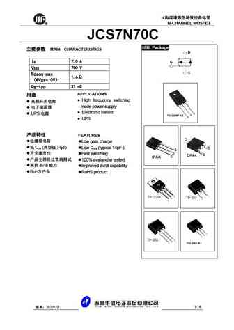
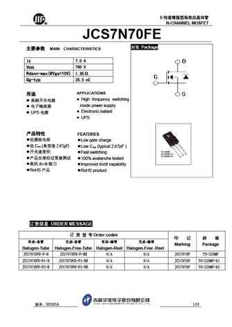
N R N-CHANNEL MOSFET JCS7N70C Package MAIN CHARACTERISTICS ID 7.0 A VDSS 700 V Rdson-max 1.6 @Vgs=10V Qg-typ 31 nC APPLICATIONS High frequency switching mode power supply Electronic ballast UPS UPS FEATUR
0.10. Size:1228K jilin sino
jcs7n70fe.pdf
N R N-CHANNEL MOSFET JCS7N70FE Package MAIN CHARACTERISTICS ID 7.0 A VDSS 700 V Rdson-max(@Vgs=10V) 1.35 Qg-typ 25.3 nC APPLICATIONS High frequency switching mode power supply Electronic ballast UPS UPS FEATURES
0.11. Size:347K crhj
cs7n70 ard.pdf

Silicon N-Channel Power MOSFET R CS7N70 ARD General Description VDSS 700 V CS7N70 ARD, the silicon N-channel Enhanced VDMOSFETs, is ID 7 A PD(TC=25 ) 100 W obtained by the self-aligned planar Technology which reduce the RDS(ON)Typ 1.5 conduction loss, improve switching performance and enhance the avalanche energy. The transistor can be used in various power
0.12. Size:1179K cn wxdh
b7n70.pdf
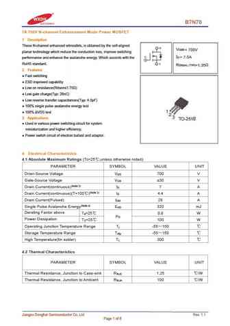
B7N70 7A 700V N-channel Enhancement Mode Power MOSFET 1 Description These N-channel enhanced vdmosfets, is obtained by the self-aligned V DSS = 700V planar technology which reduce the conduction loss, improve switching I = 7.0A D performance and enhance the avalanche energy. Which accords with the RoHS standard. R DS(on) TYP) =1.35 2 Features Fast switching ESD impro
0.13. Size:1281K cn wxdh
f7n70.pdf
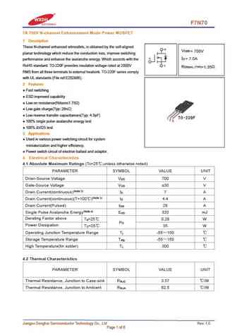
F7N70 7A 700V N-channel Enhancement Mode Power MOSFET 1 Description These N-channel enhanced vdmosfets, is obtained by the self-aligned V DSS = 700V planar technology which reduce the conduction loss, improve switching I = 7.0A D performance and enhance the avalanche energy. Which accords with the RoHS standard. TO-220F provides insulation voltage rated at 2000V R DS(on) TYP) =1.
0.14. Size:1210K cn wxdh
d7n70.pdf
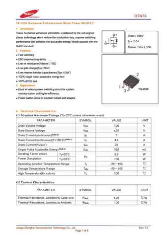
D7N70 7A 700V N-channel Enhancement Mode Power MOSFET 1 Description These N-channel enhanced vdmosfets, is obtained by the self-aligned V DSS = 700V planar technology which reduce the conduction loss, improve switching I = 7.0A D performance and enhance the avalanche energy. Which accords with the RoHS standard. R DS(on) TYP) =1.35 2 Features Fast switching ESD impro
0.16. Size:403K silan
svs7n70d.pdf
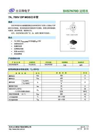
SVS7N70D 7A, 700V DP MOS SVS7N70D N MOSFET DP MOS SVS7N70D / 7A,700V, RDS(on)( )=0.52 @VGS=10V
0.19. Size:862K belling
bl7n70a-d bl7n70a-u bl7n70a-p bl7n70a-a.pdf
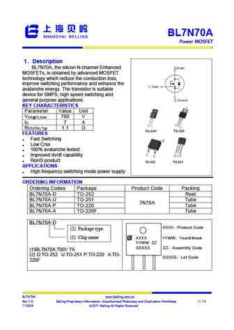
BL7N70A Power MOSFET 1 Description Step-Down Converter BL7N70A, the silicon N-channel Enhanced , MOSFETs, is obtained by advanced MOSFET technology which reduce the conduction loss, improve switching performance and enhance the avalanche energy. The transistor is suitable device for SMPS, high speed switching and general purpose applications. KEY CHARACTERISTICS Pa
0.20. Size:1127K belling
bl7n70-p bl7n70-a bl7n70-u bl7n70-d.pdf
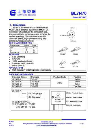
BL7N70 Power MOSFET 1 Description Step-Down Converter BL7N70, the silicon N-channel Enhanced , MOSFETs, is obtained by advanced MOSFET technology which reduce the conduction loss, improve switching performance and enhance the avalanche energy. The transistor is suitable device for SMPS, high speed switching and general purpose applications. KEY CHARACTERISTICS Para
0.21. Size:1248K maple semi
slp7n70c slf7n70c.pdf
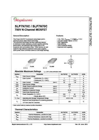
SLP7N70C / SLF7N70C 700V N-Channel MOSFET General Description Features This Power MOSFET is produced using Maple semi s - 7.0A, 700V, RDS(on)typ = 1.5 @VGS = 10 V advanced planar stripe DMOS technology. - Low gate charge ( typical 23 nC) This advanced technology has been especially tailored - High ruggedness to minimize on-state resistance, provide superior switching - Fast switching
0.22. Size:970K samwin
swf7n70k swi7n70k swd7n70k swp7n70k swj7n70k.pdf
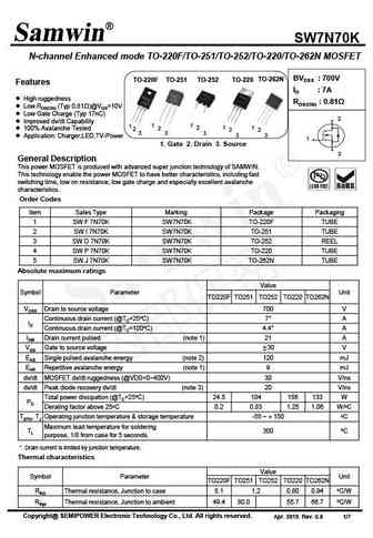
SW7N70K N-channel Enhanced mode TO-220F/TO-251/TO-252/TO-220/TO-262N MOSFET BVDSS 700V TO-262N TO-220F TO-251 TO-252 TO-220 Features ID 7A High ruggedness RDS(ON) 0.81 Low RDS(ON) (Typ 0.81 )@VGS=10V Low Gate Charge (Typ 17nC) 2 Improved dv/dt Capability 1 1 1 2 2 1 1 2 100% Avalanche Tested 2 2 3 3 3 3 3 Application
0.23. Size:972K samwin
sw7n70d swd7n70d swn7n70d swj7n70d swf7n70d.pdf
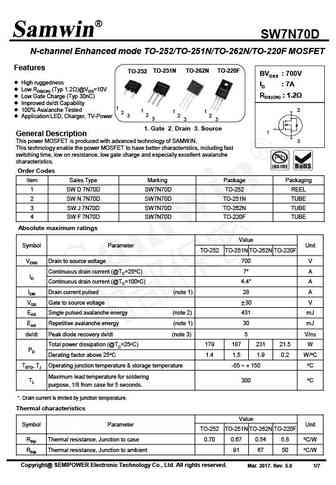
SW7N70D N-channel Enhanced mode TO-252/TO-251N/TO-262N/TO-220F MOSFET Features TO-262N TO-220F TO-251N TO-252 BVDSS 700V High ruggedness ID 7A Low RDS(ON) (Typ 1.2 )@VGS=10V RDS(ON) 1.2 Low Gate Charge (Typ 30nC) Improved dv/dt Capability 1 100% Avalanche Tested 2 1 1 1 2 2 3 2 2 Application LED, Charger, TV-Power 3
0.24. Size:1002K samwin
swd7n70d swn7n70d swj7n70d swf7n70d.pdf

SW7N70D N-channel Enhanced mode TO-252/TO-251N/TO-262N/TO-220F MOSFET Features TO-262N TO-220F TO-251N TO-252 BVDSS 700V High ruggedness ID 7A Low RDS(ON) (Typ 1.2 )@VGS=10V RDS(ON) 1.2 Low Gate Charge (Typ 30nC) Improved dv/dt Capability 1 100% Avalanche Tested 2 1 1 1 2 2 3 2 2 Application LED, Charger, TV-Power 3
0.25. Size:611K samwin
swt47n70k.pdf
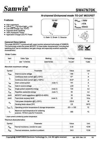
SW47N70K N-channel Enhanced mode TO-247 MOSFET Features TO-247 BVDSS 700V ID 47A High ruggedness Low RDS(ON) (Typ 65m )@VGS=10V RDS(ON) 65m Low Gate Charge (Typ 152nC) Improved dv/dt Capability 2 1 100% Avalanche Tested 2 3 Application Charger,LED,PC Power 1 1. Gate 2. Drain 3. Source 3 General Description This power MO
0.26. Size:191K semihow
hcd7n70s.pdf
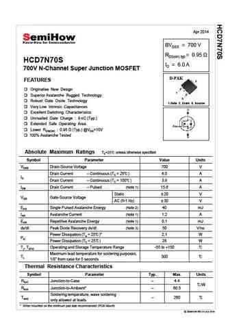
Apr 2014 BVDSS = 700 V RDS(on) typ = 0.95 HCD7N70S ID = 6.0 A 700V N-Channel Super Junction MOSFET D-PAK FEATURES 2 Originative New Design 1 Superior Avalanche Rugged Technology 3 Robust Gate Oxide Technology 1.Gate 2. Drain 3. Source Very Low Intrinsic Capacitances Excellent Switching Characteristics Unrivalled Gate Charge 9 nC (Typ.) Extended Safe Operatin
0.27. Size:661K way-on
wmm07n70c4 wml07n70c4 wmo07n70c4 wmn07n70c4 wmp07n70c4 wmk07n70c4.pdf
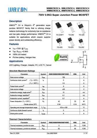
WMM0 70C4, MO07N70C 07N70C4, WML07N7 WM C4 WMN0 70C4, MK07N70C 07N70C4, WMP07N7 WM C4 700V 0.96 S T V Super Junction Power MOSFET Descrip ption WMOSTM C4 is Wa 4th generation super ayon s n junction MOSFET fa that is utilizing charge M amily S balance te or extremely esistance echnology fo y low on-re D S D G G G S D G and low ga charge performanc WM
0.28. Size:347K wuxi china
cs7n70ard.pdf
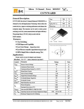
Silicon N-Channel Power MOSFET R CS7N70 ARD General Description VDSS 700 V CS7N70 ARD, the silicon N-channel Enhanced VDMOSFETs, is ID 7 A PD(TC=25 ) 100 W obtained by the self-aligned planar Technology which reduce the RDS(ON)Typ 1.5 conduction loss, improve switching performance and enhance the avalanche energy. The transistor can be used in various power
0.29. Size:397K wuxi china
cs7n70a4r-g.pdf
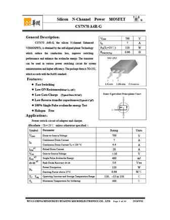
Silicon N-Channel Power MOSFET R CS7N70 A4R-G General Description VDSS 700 V CS7N70 A4R-G, the silicon N-channel Enhanced ID 7 A PD(TC=25 ) 120 W VDMOSFETs, is obtained by the self-aligned planar Technology RDS(ON)Typ 0.96 which reduce the conduction loss, improve switching performance and enhance the avalanche energy. The transistor can be used in various
0.30. Size:429K convert
cs7n70f cs7n70u.pdf
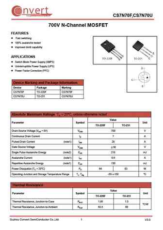
nvert Suzhou Convert Semiconductor Co ., Ltd. CS7N70F,CS7N70U 700V N-Channel MOSFET FEATURES Fast switching 100% avalanche tested Improved dv/dt capability APPLICATIONS Switch Mode Power Supply (SMPS) Uninterruptible Power Supply (UPS) Power Factor Correction (PFC) Device Marking and Package Information Device Package Marking CS7N70F TO-220F CS7N70F CS7N70
0.31. Size:513K cn hmsemi
hms7n70i hms7n70k.pdf
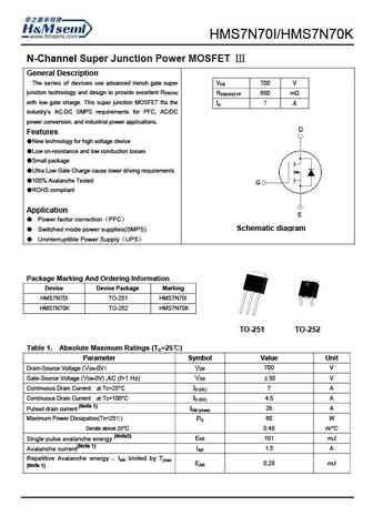
N-Channel Super Junction Power MOSFET General Description The series of devices use advanced trench gate super V 700 V DS junction technology and design to provide excellent RDS(ON) R 680 m DS(ON)TYP with low gate charge. This super junction MOSFET fits the ID 7 A industry s AC-DC SMPS requirements for PFC, AC/DC power conversion, and industrial powe
0.32. Size:244K inchange semiconductor
aotf7n70.pdf
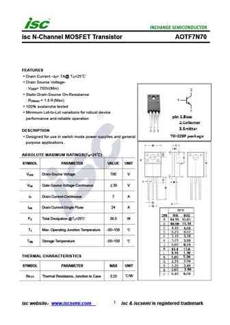
isc N-Channel MOSFET Transistor AOTF7N70 FEATURES Drain Current I = 7A@ T =25 D C Drain Source Voltage- V = 700V(Min) DSS Static Drain-Source On-Resistance R = 1.8 (Max) DS(on) 100% avalanche tested Minimum Lot-to-Lot variations for robust device performance and reliable operation DESCRIPTION Designed for use in switch mode power supplies and general purpos
0.33. Size:241K inchange semiconductor
dmj7n70sk3.pdf
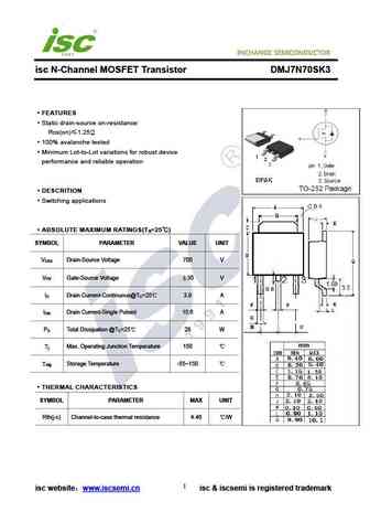
isc N-Channel MOSFET Transistor DMJ7N70SK3 FEATURES Static drain-source on-resistance RDS(on) 1.25 100% avalanche tested Minimum Lot-to-Lot variations for robust device performance and reliable operation DESCRITION Switching applications ABSOLUTE MAXIMUM RATINGS(T =25 ) a SYMBOL PARAMETER VALUE UNIT V Drain-Source Voltage 700 V DSS V Gate-Source Voltage 30
0.34. Size:261K inchange semiconductor
aot7n70.pdf
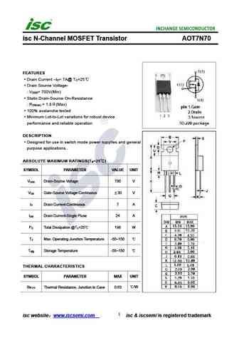
isc N-Channel MOSFET Transistor AOT7N70 FEATURES Drain Current I = 7A@ T =25 D C Drain Source Voltage- V = 700V(Min) DSS Static Drain-Source On-Resistance R = 1.8 (Max) DS(on) 100% avalanche tested Minimum Lot-to-Lot variations for robust device performance and reliable operation DESCRIPTION Designed for use in switch mode power supplies and general purpose
Otros transistores... 2N70K
, 3N70
, 3N70A
, 3N70K
, 4N70
, 4N70K
, 5N70K
, 6N70
, IRFB3607
, 8N70
, 9N70
, 10N70
, 12N70
, 15N70
, 6N65Z
, 7N65A
, 7N65
.