20N65 Datasheet. Equivalente. Reemplazo. Hoja de especificaciones. Principales características
Número de Parte: 20N65 📄📄
Tipo de FET: MOSFET
Polaridad de transistor: N
ESPECIFICACIONES MÁXIMAS
Pdⓘ - Máxima disipación de potencia: 416 W
|Vds|ⓘ - Voltaje máximo drenador-fuente: 650 V
|Vgs|ⓘ - Voltaje máximo fuente-puerta: 30 V
|Id|ⓘ - Corriente continua de drenaje: 20 A
Tjⓘ - Temperatura máxima de unión: 150 °C
CARACTERÍSTICAS ELÉCTRICAS
trⓘ - Tiempo de subida: 130 nS
Cossⓘ - Capacitancia de salida: 300 pF
RDSonⓘ - Resistencia estado encendido drenaje a fuente: 0.32 Ohm
📄📄 Copiar
Búsqueda de reemplazo de 20N65 MOSFET
- Selecciónⓘ de transistores por parámetros
20N65 datasheet
20n65.pdf

UNISONIC TECHNOLOGIES CO., LTD 20N65 Power MOSFET 20A, 650V N-CHANNEL POWER MOSFET DESCRIPTION The UTC 20N65 is an N-channel enhancement mode power MOSFET using UTC s advanced technology to provide customers with planar stripe and DMOS technology. This technology is specialized in allowing a minimum on-state resistance and superior switching performance. It also can withst
20n65.pdf
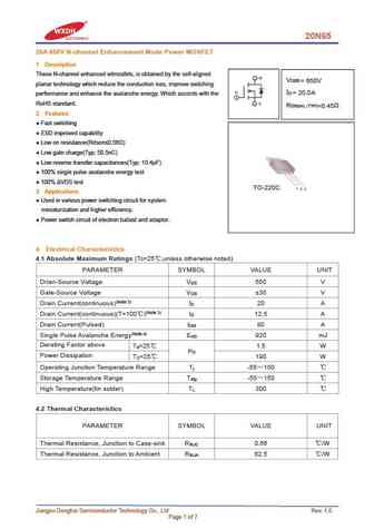
20N65 20A 650V N-channel Enhancement Mode Power MOSFET 1 Description These N-channel enhanced vdmosfets, is obtained by the self-aligned V DSS = 650V planar technology which reduce the conduction loss, improve switching I = 20.0A D performance and enhance the avalanche energy. Which accords with the RoHS standard. R DS(on) TYP) =0.45 2 Features Fast switching ESD imp
stf20n65m5 stfi20n65m5.pdf
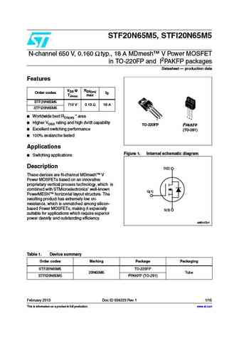
STF20N65M5, STFI20N65M5 N-channel 650 V, 0.160 typ., 18 A MDmesh V Power MOSFET in TO-220FP and I2PAKFP packages Datasheet production data Features VDS @ RDS(on) Order codes ID TJmax max STF20N65M5 710 V 0.19 18 A STFI20N65M5 3 Worldwide best RDS(on) * area 1 2 2 3 1 Higher VDSS rating and high dv/dt capability TO-220FP I2PAKFP Excellent switching
stb20n65m5 sti20n65m5 stp20n65m5 stw20n65m5.pdf
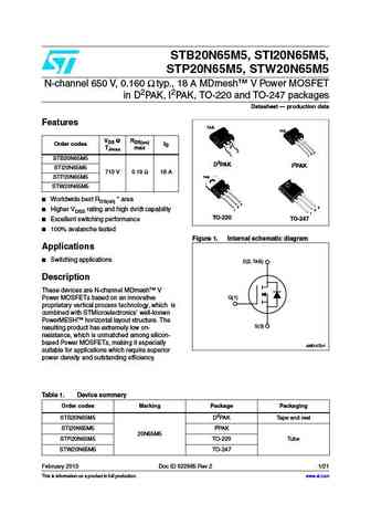
STB20N65M5, STI20N65M5, STP20N65M5, STW20N65M5 N-channel 650 V, 0.160 typ., 18 A MDmesh V Power MOSFET in D2PAK, I2PAK, TO-220 and TO-247 packages Datasheet production data Features TAB TAB VDS @ RDS(on) Order codes ID 2 TJmax max 3 3 2 1 1 STB20N65M5 D2PAK I2PAK STI20N65M5 710 V 0.19 18 A TAB STP20N65M5 STW20N65M5 Worldwide best RDS(on) * area 3 2
spp20n65c3 spa20n65c3 spi20n65c3.pdf
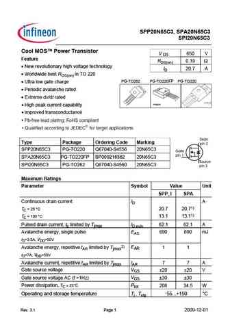
SPP20N65C3, SPA20N65C3 SPI20N65C3 Cool MOS Power Transistor V 650 V DS Feature RDS(on) 0.19 New revolutionary high voltage technology ID 20.7 A Worldwide best RDS(on) in TO 220 PG-TO262 PG-TO220FP PG-TO220 Ultra low gate charge Periodic avalanche rated 3 Extreme dv/dt rated 2 1 P-TO220-3-31 High peak current capability Improved transconducta
igp20n65f5.pdf
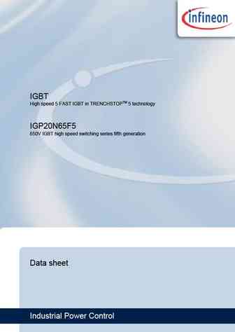
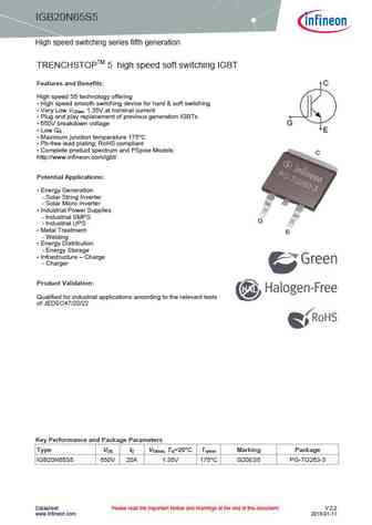
IGBT High speed 5 FAST IGBT in TRENCHSTOPTM 5 technology IGP20N65F5 650V IGBT high speed switching series fifth generation Data sheet Industrial Power Control IGP20N65F5 High speed switching series fifth generation High speed 5 FAST IGBT in TRENCHSTOPTM 5 technology Features and Benefits C High speed F5 technology offering Best-in-Class efficiency in hard switching and resonant
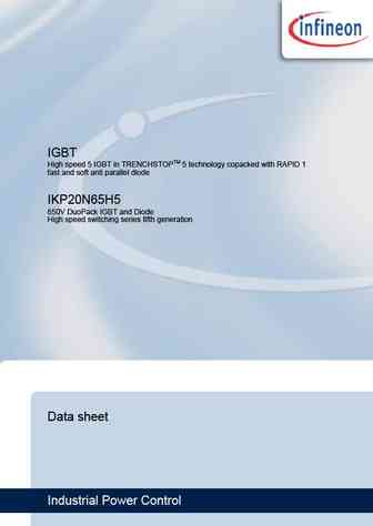
ikp20n65f5.pdf

IGBT High speed 5 FAST IGBT in TRENCHSTOPTM 5 technology copacked with RAPID 1 fast and soft anti parallel diode IKP20N65F5 650V DuoPack IGBT and Diode High speed switching series fifth generation Data sheet Industrial Power Control IKP20N65F5 High speed switching series fifth generation High speed 5 FAST IGBT in TRENCHSTOPTM 5 technology copacked with RAPID 1 fast and soft anti par
ikb20n65eh5.pdf
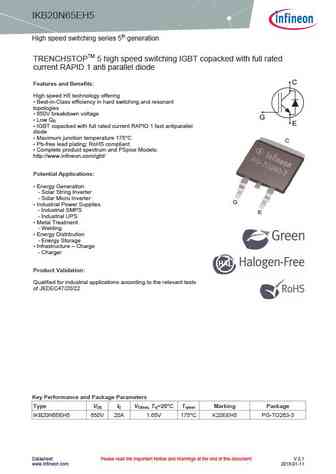
IKB20N65EH5 High speed switching series 5th generation TRENCHSTOPTM 5 high speed switching IGBT copacked with full rated current RAPID 1 anti parallel diode C Features and Benefits High speed H5 technology offering Best-in-Class efficiency in hard switching and resonant topologies 650V breakdown voltage G Low Q G E IGBT copacked with full rated current RAPID 1 fas
ikp20n65h5.pdf
IGBT High speed 5 IGBT in TRENCHSTOPTM 5 technology copacked with RAPID 1 fast and soft anti parallel diode IKP20N65H5 650V DuoPack IGBT and Diode High speed switching series fifth generation Data sheet Industrial Power Control IKP20N65H5 High speed switching series fifth generation High speed 5 IGBT in TRENCHSTOPTM 5 technology copacked with RAPID 1 fast and soft anti parallel diod
ihw20n65r5.pdf
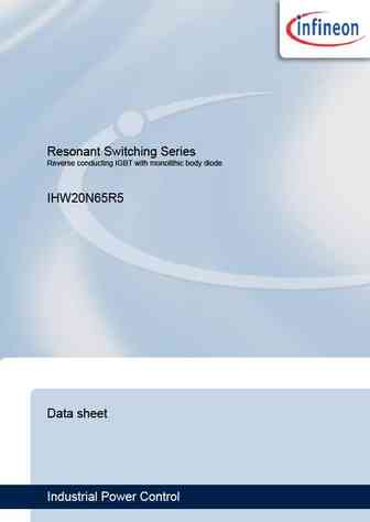
Resonant Switching Series Reverse conducting IGBT with monolithic body diode IHW20N65R5 Data sheet Industrial Power Control IHW20N65R5 Resonant Switching Series Reverse conducting IGBT with monolithic body diode C Features Powerful monolithic reverse-conducting diode with low forward voltage TRENCHSTOPTM technology offers - very tight parameter distribution G - high ru
igp20n65h5.pdf

IGBT High speed 5 IGBT in TRENCHSTOPTM 5 technology IGP20N65H5 650V IGBT high speed switching series fifth generation Data sheet Industrial Power Control IGP20N65H5 High speed switching series fifth generation High speed 5 IGBT in TRENCHSTOPTM 5 technology Features and Benefits C High speed H5 technology offering Best-in-Class efficiency in hard switching and resonant topologi
igb20n65s5.pdf
IGB20N65S5 High speed switching series fifth generation TRENCHSTOPTM 5 high speed soft switching IGBT Features and Benefits C High speed S5 technology offering High speed smooth switching device for hard & soft switching Very Low V , 1.35V at nominal current CEsat Plug and play replacement of previous generation IGBTs 650V breakdown voltage G Low Q E G Maxim
ixyp20n65c3d1.pdf

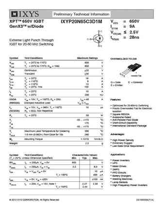
XPTTM 650V IGBT VCES = 650V IXYA20N65C3D1 GenX3TM w/Diode IC110 = 20A IXYP20N65C3D1 VCE(sat) 2.50V tfi(typ) = 28ns Extreme Light Punch Through IGBT for 20-60kHz Switching TO-263 AA (IXYA) G Symbol Test Conditions Maximum Ratings E VCES TJ = 25 C to 175 C 650 V C (Tab) VCGR TJ = 25 C to 175 C, RGE = 1M
ixyn120n65b3d1.pdf
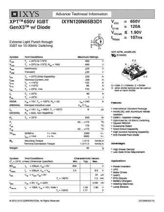
Advance Technical Information VCES = 650V XPTTM 650V IGBT IXYN120N65B3D1 IC110 = 120A GenX3TM w/ Diode VCE(sat) 1.90V tfi(typ) = 107ns Extreme Light Punch through IGBT for 10-30kHz Switching E SOT-227B, miniBLOC E153432 Symbol Test Conditions Maximum Ratings E VCES TJ = 25 C to 175 C 650 V G VCGR TJ
ixfk120n65x2 ixfx120n65x2.pdf
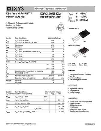
Advance Technical Information X2-Class HiPerFETTM VDSS = 650V IXFK120N65X2 Power MOSFET ID25 = 120A IXFX120N65X2 RDS(on) 24m N-Channel Enhancement Mode Avalanche Rated Fast Intrinsic Diode TO-264P (IXFK) Symbol Test Conditions Maximum Ratings G VDSS TJ = 25 C to 150 C 650 V D Tab VDGR TJ = 25 C to 150 C, RGS = 1M 650 V S VGSS
ixyh20n65b3.pdf
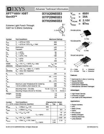
Advance Technical Information XPTTM 650V IGBT VCES = 650V IXYA20N65B3 GenX3TM IC110 = 20A IXYP20N65B3 VCE(sat) 2.10V IXYH20N65B3 tfi(typ) = 87ns Extreme Light Punch Through IGBT for 5-30kHz Switching TO-263 (IXYA) G E C (Tab) Symbol Test Conditions Maximum Ratings TO-220 (IXYP) VCES TJ = 25 C to 175 C 650
ixyp20n65b3.pdf

Advance Technical Information XPTTM 650V IGBT VCES = 650V IXYA20N65B3 GenX3TM IC110 = 20A IXYP20N65B3 VCE(sat) 2.10V IXYH20N65B3 tfi(typ) = 87ns Extreme Light Punch Through IGBT for 5-30kHz Switching TO-263 (IXYA) G E C (Tab) Symbol Test Conditions Maximum Ratings TO-220 (IXYP) VCES TJ = 25 C to 175 C 650
ixya20n65b3.pdf

Advance Technical Information XPTTM 650V IGBT VCES = 650V IXYA20N65B3 GenX3TM IC110 = 20A IXYP20N65B3 VCE(sat) 2.10V IXYH20N65B3 tfi(typ) = 87ns Extreme Light Punch Through IGBT for 5-30kHz Switching TO-263 (IXYA) G E C (Tab) Symbol Test Conditions Maximum Ratings TO-220 (IXYP) VCES TJ = 25 C to 175 C 650
ixtp20n65xm.pdf
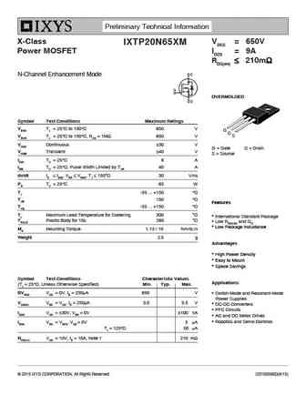
Preliminary Technical Information X-Class VDSS = 650V IXTP20N65XM Power MOSFET ID25 = 9A RDS(on) 210m N-Channel Enhancement Mode OVERMOLDED Symbol Test Conditions Maximum Ratings VDSS TJ = 25 C to 150 C 650 V G D S VDGR TJ = 25 C to 150 C, RGS = 1M 650 V VGSS Continuous 30 V G = Gate D = Drain VGSM Transient 40 V S = So
ixta20n65x ixth20n65x ixtp20n65x.pdf
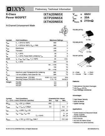
Preliminary Technical Information X-Class VDSS = 650V IXTA20N65X Power MOSFET ID25 = 20A IXTP20N65X RDS(on) 210m IXTH20N65X N-Channel Enhancement Mode TO-263 (IXTA) G S D (Tab) Symbol Test Conditions Maximum Ratings TO-220 (IXTP) VDSS TJ = 25 C to 150 C 650 V VDGR TJ = 25 C to 150 C, RGS = 1M 650 V VGSS Continuous 30 V VG
ixyh120n65c3.pdf
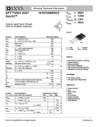
Advance Technical Information VCES = 650V XPTTM 650V IGBT IXYH120N65C3 IC110 = 120A GenX3TM VCE(sat) 2.8V tfi(typ) = 46ns Extreme Light Punch Through IGBT for 20-60kHz Switching TO-247 Symbol Test Conditions Maximum Ratings VCES TJ = 25 C to 175 C 650 V G VCGR TJ = 25 C to 175 C, RGE = 1M 650 V C Tab
ixya20n65c3.pdf

Preliminary Technical Information XPTTM 650V IGBT VCES = 650V IXYA20N65C3 GenX3TM IC110 = 20A IXYH20N65C3 VCE(sat) 2.50V tfi(typ) = 28ns Extreme Light Punch Through IGBT for 20-60 kHz Switching TO-263 AA (IXYA) Symbol Test Conditions Maximum Ratings G E VCES TJ = 25 C to 175 C 650 V C (Tab) VCGR TJ = 25 C
ixyn120n65c3d1.pdf
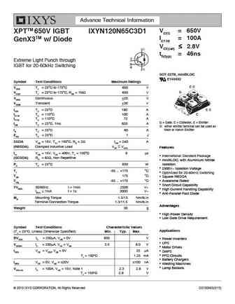
Advance Technical Information VCES = 650V XPTTM 650V IGBT IXYN120N65C3D1 IC110 = 100A GenX3TM w/ Diode VCE(sat) 2.8V tfi(typ) = 46ns Extreme Light Punch through IGBT for 20-60kHz Switching E SOT-227B, miniBLOC E153432 Symbol Test Conditions Maximum Ratings E VCES TJ = 25 C to 175 C 650 V G VCGR TJ =
ixyh20n65c3.pdf
Preliminary Technical Information XPTTM 650V IGBT VCES = 650V IXYA20N65C3 GenX3TM IC110 = 20A IXYH20N65C3 VCE(sat) 2.50V tfi(typ) = 28ns Extreme Light Punch Through IGBT for 20-60 kHz Switching TO-263 AA (IXYA) Symbol Test Conditions Maximum Ratings G E VCES TJ = 25 C to 175 C 650 V C (Tab) VCGR TJ = 25 C
ixya20n65c3d1.pdf
XPTTM 650V IGBT VCES = 650V IXYA20N65C3D1 GenX3TM w/Diode IC110 = 20A IXYP20N65C3D1 VCE(sat) 2.50V tfi(typ) = 28ns Extreme Light Punch Through IGBT for 20-60kHz Switching TO-263 AA (IXYA) G Symbol Test Conditions Maximum Ratings E VCES TJ = 25 C to 175 C 650 V C (Tab) VCGR TJ = 25 C to 175 C, RGE = 1M
ixtk120n65x2 ixtx120n65x2.pdf
Advance Technical Information X2-Class VDSS = 650V IXTK120N65X2 Power MOSFET ID25 = 120A IXTX120N65X2 RDS(on) 24m N-Channel Enhancement Mode Avalanche Rated TO-264P (IXTK) Symbol Test Conditions Maximum Ratings G VDSS TJ = 25 C to 150 C 650 V D Tab VDGR TJ = 25 C to 150 C, RGS = 1M 650 V S VGSS Continuous 30 V PLUS247 (IX
ixyp20n65b3d1.pdf
Advance Technical Information XPTTM 650V IGBT VCES = 650V IXYP20N65B3D1 GenX3TM w/Diode IC110 = 20A VCE(sat) 2.10V tfi(typ) = 87ns Extreme Light Punch Through IGBT for 5-30kHz Switching TO-220 Symbol Test Conditions Maximum Ratings G VCES TJ = 25 C to 175 C 650 V C Tab E VCGR TJ = 25 C to 175 C, RGE = 1M
ixyh120n65b3.pdf

Advance Technical Information VCES = 650V XPTTM 650V IGBT IXYH120N65B3 IC110 = 120A GenX3TM VCE(sat) 1.90V tfi(typ) = 107ns Extreme Light Punch Through IGBT for 10-30kHz Switching TO-247 Symbol Test Conditions Maximum Ratings VCES TJ = 25 C to 175 C 650 V G VCGR TJ = 25 C to 175 C, RGE = 1M 650 V C T
ixyp20n65c3d1m.pdf
Preliminary Technical Information XPTTM 650V IGBT VCES = 650V IXYP20N65C3D1M GenX3TM w/Diode IC110 = 9A VCE(sat) 2.5V tfi(typ) = 28ns Extreme Light Punch Through IGBT for 20-60 kHz Switching Symbol Test Conditions Maximum Ratings OVERMOLDED TO-220 VCES TJ = 25 C to 175 C 650 V VCGR TJ = 25 C to 175 C, RGE =
jcs20n65fei.pdf
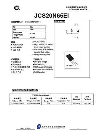
N R N-CHANNEL MOSFET JCS20N65EI Package MAIN CHARACTERISTICS ID 20A VDSS 650V Rdson-max 0.42 Vgs=10V Qg-Typ 64.6nC APPLICATIONS High efficiency switch mode power supplies Electronic lamp ballasts LED based on half bridge LED power
jcs20n65fh jcs20n65wh.pdf
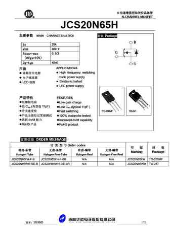
N R N-CHANNEL MOSFET JCS20N65H MAIN CHARACTERISTICS Package ID 20A VDSS 650 V Rdson-max 0.5 @Vgs=10V Qg-typ 45nC APPLICATIONS High frequency switching mode power supply Electronic ballast LED LED power supply
brfl20n65.pdf
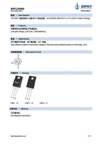
BRFL20N65 Rev.A May.-2023 DATA SHEET / Descriptions TO-220FL N MOS N-CHANNEL MOSFET in a TO-220FL Plastic Package. / Features , , Low gate charge, Low Crss , Fast switching. / Applications UPS High efficiency switch mode pow
cs20n65f a9h.pdf
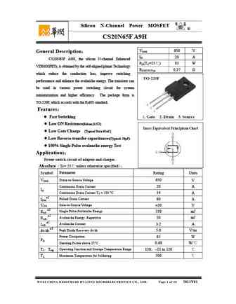
Silicon N-Channel Power MOSFET R CS20N65F A9H VDSS 650 V General Description ID 20 A CS20N65F A9H, the silicon N-channel Enhanced PD(TC=25 ) 85 W VDMOSFETs, is obtained by the self-aligned planar Technology RDS(ON)Typ 0.37 which reduce the conduction loss, improve switching performance and enhance the avalanche energy. The transistor can be used in various
20n65d.pdf
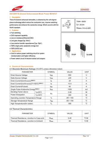
20N65D 20A 650V N-channel Enhancement Mode Power MOSFET 1 Description These N-channel enhanced vdmosfets, is obtained by the self-aligned V DSS = 650V planar technology which reduce the conduction loss, improve switching I = 20.0A D performance and enhance the avalanche energy. Which accords with the RoHS standard. R DS(on) TYP) =0.40 2 Features Fast switching ESD im
ru20n65r.pdf

RU20N65R N-Channel Advanced Power MOSFET Features Pin Description 650V/20A, RDS (ON) =400m (Typ.)@VGS=10V Low Reverse Transfer Ultra Low Gate Charge 100% avalanche tested Lead Free and Green Devices Available (RoHS Compliant) Lead Free and Green Devices Available (RoHS Compliant) G DS TO220 D D D D D Applications D pp D AC/DC Power Conversion i
ru20n65p.pdf

RU20N65P N-Channel Advanced Power MOSFET Features Pin Description 650V/20A, RDS (ON) =400m (Typ.)@VGS=10V Low Reverse Transfer Ultra Low Gate Charge 100% avalanche tested Lead Free and Green Devices Available (RoHS Compliant) Lead Free and Green Devices Available (RoHS Compliant) GD S TO220F D D D D D Applications D pp D AC/DC Power Conversion
bl20n65-p bl20n65-a bl20n65-w bl20n65-f.pdf
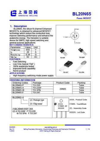
BL20N65 Power MOSFET 1 Description Step-Down Converter BL20N65, the silicon N-channel Enhanced , MOSFETs, is obtained by advanced MOSFET technology which reduce the conduction loss, improve switching performance and enhance the avalanche energy. The transistor is suitable device for SMPS, high speed switching and general purpose applications. KEY CHARACTERISTICS Pa
jfpc20n65c.pdf

JFPC20N65C 650V N-Channel MOSFET General Description This Power MOSFET is produced using advanced planar stripe DMOS technology. This advanced technology has been especially tailored to minimize on-state resistance, provide superior switching performance, and withstand high energy pulse in the avalanche and commutation mode. These devices are well suited for high efficiency
jffc20n65c.pdf
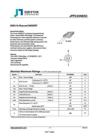
JFFC20N65C 650V N-Channel MOSFET General Description This Power MOSFET is produced using advanced planar stripe DMOS technology. This advanced technology has been especially tailored to minimize on-state resistance, provide superior switching performance, and withstand high energy pulse in the avalanche and commutation mode. These devices are well suited for high efficiency
jfam20n65c.pdf

JFAM20N65C 650V N-Channel MOSFET General Description This Power MOSFET is produced using advanced planar stripe DMOS technology. This advanced technology has been especially tailored to minimize on-state resistance, provide superior switching performance, and withstand high energy pulse in the avalanche and commutation mode. These devices are well suited for high efficiency
jfam20n65e.pdf

JFAM20N65E 650V N-Channel MOSFET General Description This Power MOSFET is produced using advanced planar stripe DMOS technology. This advanced technology has been especially tailored to minimize on-state resistance, provide superior switching performance, and withstand high energy pulse in the avalanche and commutation mode. These devices are well suited for high efficiency
ost120n65h4smf.pdf
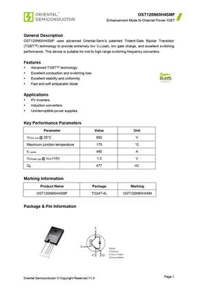
OST120N65H4SMF Enhancement Mode N-Channel Power IGBT General Description OST120N65H4SMF uses advanced Oriental-Semi s patented Trident-Gate Bipolar Transistor (TGBTTM) technology to provide extremely low V (sat), low gate charge, and excellent switching CE performance. This device is suitable for mid to high range switching frequency converters. Features Advanced TGBTTM tec
ost120n65h5smf.pdf
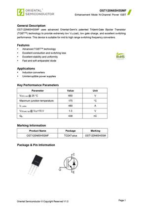
OST120N65H5SMF Enhancement Mode N-Channel Power IGBT General Description OST120N65H5SMF uses advanced Oriental-Semi s patented Trident-Gate Bipolar Transistor (TGBTTM) technology to provide extremely low V (sat), low gate charge, and excellent switching CE performance. This device is suitable for mid to high range switching frequency converters. Features Advanced TGBTTM tec
ost120n65hemf.pdf
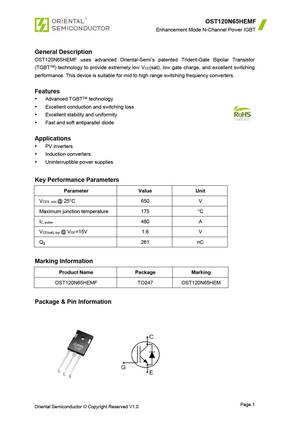
OST120N65HEMF Enhancement Mode N-Channel Power IGBT General Description OST120N65HEMF uses advanced Oriental-Semi s patented Trident-Gate Bipolar Transistor (TGBTTM) technology to provide extremely low V (sat), low gate charge, and excellent switching CE performance. This device is suitable for mid to high range switching frequency converters. Features Advanced TGBTTM techn
ost120n65h4umf.pdf
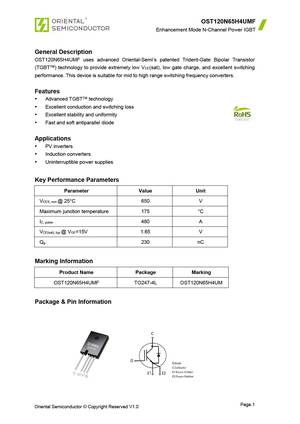
OST120N65H4UMF Enhancement Mode N-Channel Power IGBT General Description OST120N65H4UMF uses advanced Oriental-Semi s patented Trident-Gate Bipolar Transistor (TGBTTM) technology to provide extremely low V (sat), low gate charge, and excellent switching CE performance. This device is suitable for mid to high range switching frequency converters. Features Advanced TGBTTM tec
ptp20n65a pta20n65a.pdf
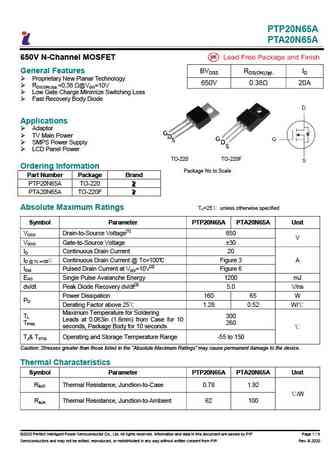
PTP20N65A PTA20N65A 650V N-Channel MOSFET General Features BVDSS RDS(ON),typ. ID Proprietary New Planar Technology 650V 0.38 20A RDS(ON),typ.=0.38 @VGS=10V Low Gate Charge Minimize Switching Loss Fast Recovery Body Diode Applications Adaptor G TV Main Power D S G D SMPS Power Supply S LCD Panel Power TO-220 TO-220F Ordering Information Packa
swf20n65d swt20n65d.pdf
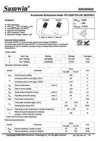
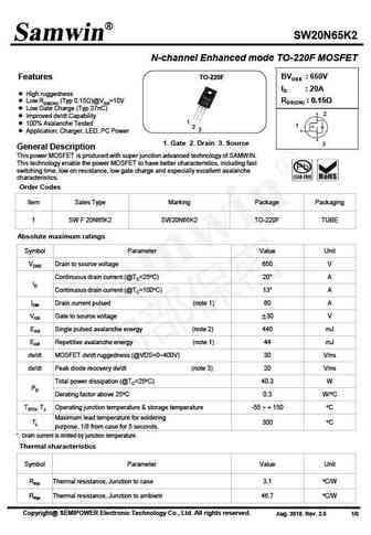
SW20N65D N-channel Enhanced mode TO-220F/TO-247 MOSFET TO-220F TO-247 BVDSS 650V Features ID 20A High ruggedness RDS(ON) 0.31 Low RDS(ON) (Typ 0.31 )@VGS=10V Low Gate Charge (Typ 88nC) 2 Improved dv/dt Capability 1 1 100% Avalanche Tested 2 2 1 3 3 Application Charger, Adaptor, LED 1. Gate 2. Drain 3. Source 3 General Desc
swp20n65k swf20n65k sww20n65k swj20n65k.pdf
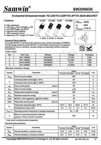
SW20N65K N-channel Enhanced mode TO-220/TO-220F/TO-3P/TO-262N MOSFET Features TO-220 TO-220F TO-3P TO-262N BVDSS 650V High ruggedness ID 20A Low RDS(ON) (Typ 0.16 )@VGS=10V RDS(ON) 0.16 Low Gate Charge (Typ 60nC) Improved dv/dt Capability 2 100% Avalanche Tested 1 1 1 1 2 2 2 2 Application LED, Charger, PC Power 3 3 3 3 1. Gat
swf20n65k2.pdf

SW20N65K2 N-channel Enhanced mode TO-220F MOSFET TO-220F BVDSS 650V Features ID 20A High ruggedness RDS(ON) 0.15 Low RDS(ON) (Typ 0.15 )@VGS=10V Low Gate Charge (Typ 37nC) 2 Improved dv/dt Capability 1 100% Avalanche Tested 1 2 3 Application Charger, LED, PC Power 1. Gate 2. Drain 3. Source 3 General Description This
sw20n65k2 swf20n65k2.pdf
SW20N65K2 N-channel Enhanced mode TO-220F MOSFET TO-220F BVDSS 650V Features ID 20A High ruggedness RDS(ON) 0.15 Low RDS(ON) (Typ 0.15 )@VGS=10V Low Gate Charge (Typ 37nC) 2 Improved dv/dt Capability 1 100% Avalanche Tested 1 2 3 Application Charger, LED, PC Power 1. Gate 2. Drain 3. Source 3 General Description This
srm20n65.pdf
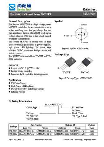
Datasheet 20A, 650V, N-Channel Power MOSFET SRM20N65 General Description Symbol The Sanrise SRM20N65 is a high voltage power MOSFET, which has better characteristics, such as fast switching time, low gate charge, low on- state resistance. Sanrise SRM20N65 break down voltage rating is 650V and it has a high rugged avalanche characteristics. This power MOSFET is usually used at hi
tsf20n65mr.pdf

TSF20N65MR 650V N-Channel MOSFET General Description Features This Power MOSFET is produced using Truesemi s 20A,650V,RDS(on)=0.48 @ VGS =10V advanced planar stripe DMOS technology. This advanced technology has been especially tailored to Low gate charge(typical 57nC) minimize on-state resistance, provide superior switching High ruggedness performance, and with
tsa20n65mr.pdf
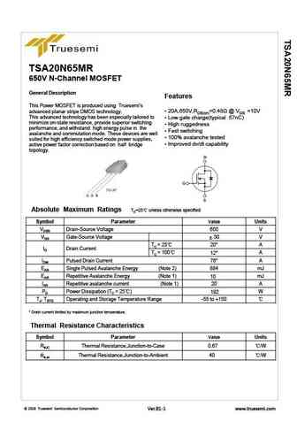
TSA20N65MR 650V N-Channel MOSFET General Description Features This Power MOSFET is produced using Truesemi s 20A,650V,RDS(on)=0.48 @ VGS =10V advanced planar stripe DMOS technology. This advanced technology has been especially tailored to Low gate charge(typical 57nC) minimize on-state resistance, provide superior switching High ruggedness performance, and with
cs20n65fa9h.pdf
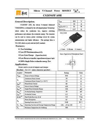
Silicon N-Channel Power MOSFET R CS20N65F A9H VDSS 650 V General Description ID 20 A CS20N65F A9H, the silicon N-channel Enhanced PD(TC=25 ) 85 W VDMOSFETs, is obtained by the self-aligned planar Technology RDS(ON)Typ 0.37 which reduce the conduction loss, improve switching performance and enhance the avalanche energy. The transistor can be used in various
cs20n65f cs20n65p cs20n65v cs20n65w.pdf
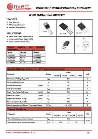
nvert CS20N65F,CS20N65P,CS20N65V,CS20N65W Suzhou Convert Semiconductor Co ., Ltd. 650V N-Channel MOSFET FEATURES Fast switching 100% avalanche tested Improved dv/dt capability APPLICATIONS Switch Mode Power Supply (SMPS) Uninterruptible Power Supply (UPS) Power Factor Correction (PFC) Device Marking and Package Information Device Package Marking CS20N65F T
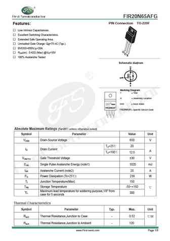
fir20n65afg.pdf
FIR20N65AFG PIN Connection TO-220F Features Low Intrinsic Capacitances. Excellent Switching Characteristics. Extended Safe Operating Area. Unrivalled Gate Charge Qg=75 nC (Typ.). BVDSS=650V,ID=20A G RDS(on) 0.42 (Max) @VG=10V D S 100% Avalanche Tested g Schematic dia ram D G S Marking Diagram Y = Year A = Assembly Location WW = Work
fir20n65fg.pdf
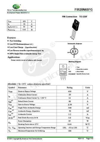
FIR20N65FG N-Channel Power MOSFET-X PIN Connection TO-220F VDSS 650 V ID 20 A PD(TC=25 ) 85 W RDS(ON)Typ 0.45 G Features DS Fast Switching g Schematic dia ram Low ON Resistance(Rdson 0.45 ) D Low Gate Charge (Typical Data 65nC) Low Reverse transfer capacitances(Typical 20p G 100% Single Pulse avalanche energy Test S Applications Power switch circuit of adapt
smf20n65.pdf
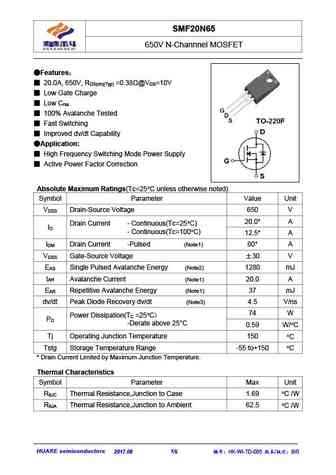
SMF20N65 650V N-Channnel MOSFET Features 20.0A, 650V, R =0.38 @V =10V DS(on)(Typ) GS Low Gate Charge Low C rss 100% Avalanche Tested Fast Switching Improved dv/dt Capability Application High Frequency Switching Mode Power Supply Active Power Factor Correction Absolute Maximum Ratings(Tc=25 C unless otherwise noted) Symbol Parameter Va
jjt20n65sc.pdf
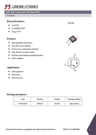
650V 20A Trench and Field Stop IGBT JJT20N65SC Key performance TO-263 V =650V CE I =20A@T =100 C C V =1.6 V CE(sat) C Features G High ruggedness performance. E 10 s short circuit capability. Positive V temperature coefficient. CE (sat) High efficiency for motor control. Excellent current sharing in parallel operation. RoHS compliant.
jjt20n65se.pdf

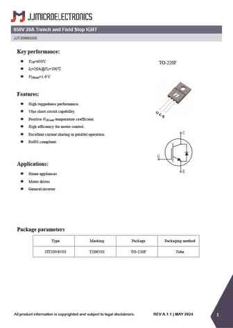
650V 20A Trench and Field Stop IGBT JJT20N65SE Key performance TO-247 V =650V CE I =20A@T =100 C C V =1.6 V CE(sat) Features G High ruggedness performance. C E 10 s short circuit capability. Positive V temperature coefficient. CE (sat) High efficiency for motor control. Excellent current sharing in parallel operation. RoHS compliant.
jjt20n65ss.pdf
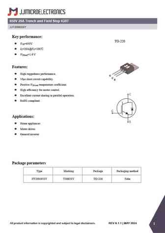
650V 20A Trench and Field Stop IGBT JJT20N65SS Key performance V =650V CE TO-220F I =20A@T =100 C C V =1.6 V CE(sat) Features High ruggedness performance. 10 s short circuit capability. G C E Positive V temperature coefficient. CE (sat) High efficiency for motor control. Excellent current sharing in parallel operation. RoHS compliant
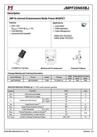
jmpf20n65bj.pdf
JMPF20N65BJ Description JMP N-channel Enhancement Mode Power MOSFET Features Applications 650V, 20A Load Switch RDS(ON)
jjt20n65sy.pdf
650V 20A Trench and Field Stop IGBT JJT20N65SY Key performance TO-220 V =650V CE I =20A@T =100 C C V =1.6 V CE(sat) Features High ruggedness performance. G C 10 s short circuit capability. E Positive V temperature coefficient. CE (sat) High efficiency for motor control. Excellent current sharing in parallel operation. RoHS compliant.
jmpc20n65bj.pdf

JMPC20N65BJ Description JMP N-channel Enhancement Mode Power MOSFET Features Applications 650V, 20A Load Switch RDS(ON)
lnc20n65 lnd20n65 lnb20n65.pdf
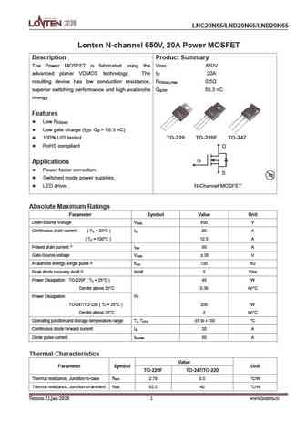
LNC20N65/LND20N65/LNB20N65 Lonten N-channel 650V, 20A Power MOSFET Description Product Summary The Power MOSFET is fabricated using the V 650V DSS advanced planer VDMOS technology. The I 20A D resulting device has low conduction resistance, R 0.5 DS(on),max superior switching performance and high avalanche Q 58.3 nC g,typ energy. Features Low R DS(on) Low gate charge (t
agm20n65f.pdf
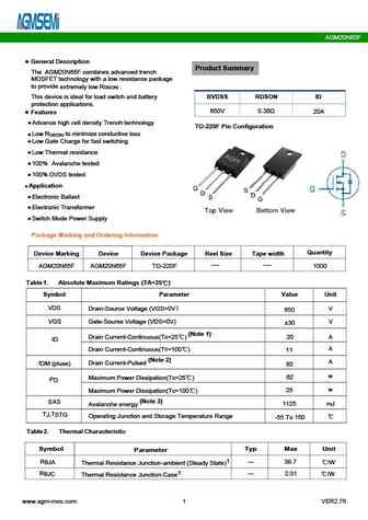
AGM20N65F General Description Product Summary The AGM20N65F combines advanced trench MOSFET technology with a low resistance package to provide extremely low R . DS(ON) This device is ideal switch and battery BVDSS RDSON ID for load protection applications. 650V 0.36 20A Features Advance high cell density Trench technology TO-220F Pin Configuration Low R to m
siw120n65g2p2d.pdf
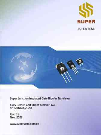
SUPER-SEMI Super Junction Insulated Gate Bipolar Transistor 650V Trench and Super Junction IGBT SI*120N65G2P2D Rev. 0.9 Nov. 2023 www.supersemi.com.cn SIW120N65G2P2D 650V Trench and Super Junction IGBT General Description Super-Semi Trench and Super Junction IGBTs, VCE 650 V designed according to the super junction (SJ) IC 120 A technology. The SJ-IGBT series provides low VCE(sa
spc20n65g.pdf
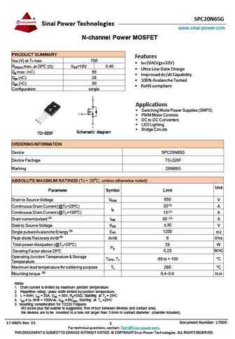
SPC20N65G Sinai Power Technologies www.sinai-power.com N-channel Power MOSFET PRODUCT SUMMARY Features V (V) at T max. 700 DS J ID=20A(Vgs=10V) R max. at 25oC ( ) V =10V 0.40 DS(on) GS Ultra Low Gate Charge Q max. (nC) 95 g Improved dv/dt Capability Q (nC) 28 gs 100% Avalanche Tested Q (nC) 30 gd RoHS compliant Configuration single
smirf20n65.pdf
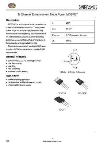
SMIRF20N65 30V /36A Single N Power MOSFET N-Channel Enhancement Mode Power MOSFET Description ID 20A IRF20N65 is an N-channel enhancement mode power MOS field effect transistor. The improved VDSS 650V planar stripe cell and the improved guard ring terminal have been especially tailored to minimize Rdson max 0.5 (VGS=10V, ID=10A) on-state resistance, provide superior s
vbzmb20n65s.pdf
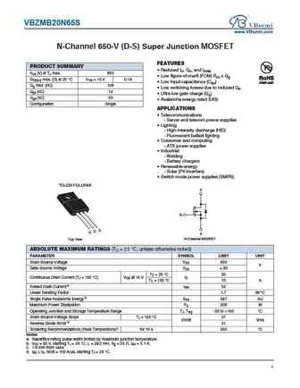
VBZMB20N65S www.VBsemi.com N-Channel 650-V (D-S) Super Junction MOSFET FEATURES PRODUCT SUMMARY Reduced trr, Qrr, and IRRM VDS (V) at TJ max. 650 Low figure-of-merit (FOM) Ron x Qg RDS(on) max. ( ) at 25 C VGS = 10 V 0.19 Low input capacitance (Ciss) Qg max. (nC) 106 Low switching losses due to reduced Qrr Qgs (nC) 14 Ultra low gate charge (Qg) Qgd (nC) 33
vbzmb20n65.pdf
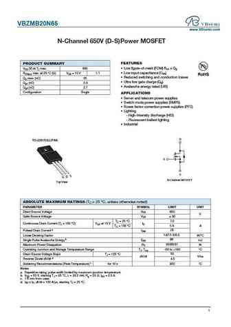
VBZMB20N65 www.VBsemi.com N hannel 650 D S Power MOSFET FEATURES PRODUCT SUMMARY VDS (V) at TJ max. 650 Low figure-of-merit (FOM) Ron x Qg Low input capacitance (Ciss) RDS(on) max. at 25 C ( ) VGS = 10 V 1.1 Reduced switching and conduction losses Qg max. (nC) 25 Ultra low gate charge (Qg) Qgs (nC) 2.0 Avalanche energy rated (UIS) Qgd (nC) 2.7 Configura
dgw20n65ctl.pdf
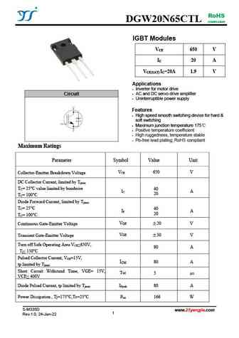
RoHS DGW20N65CTL COMPLIANT IGBT Modules IGBT Descrete V 650 V CE I 20 A C V I =20A 1.9 V CE(SAT) C Applications Inverter for motor drive AC and DC servo drive amplifier Circuit Uninterruptible power supply Features High speed smooth switching device for hard & soft switching Maximum junction temperature 175 Positive temperature
tma20n65h tmp20n65h.pdf
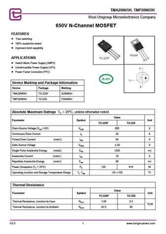
TMA20N65H, TMP20N65H Wuxi Unigroup Microelectronics Company 650V N-Channel MOSFET FEATURES Fast switching 100% avalanche tested Improved dv/dt capability APPLICATIONS Switch Mode Power Supply (SMPS) Uninterruptible Power Supply (UPS) Power Factor Correction (PFC) Device Marking and Package Information Device Package Marking TMA20N65H TO-220F A2
tma20n65hg tmw20n65hg.pdf
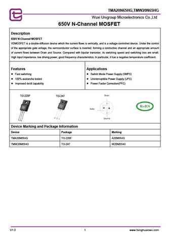
TMA20N65HG,TMW20N65HG Wuxi Unigroup Microelectronics Co.,Ltd 650V N-Channel MOSFET Description 650V N-Channel MOSFET VDMOSFET is a double-diffusion device which the current flows is vertically, and is a voltage-controlled device. Under the control of the appropriate gate voltage, the semiconductor surface is inverted, forming a conductive channel and an appropriate amount of curre
hmg20n65f.pdf
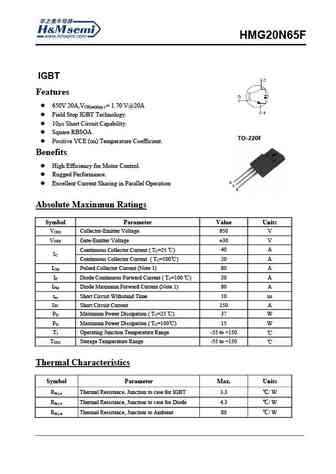
HMG20N65F IGBT Features 650V 20A,V = 1.70 V@20A CE(sat)(typ.) Field Stop IGBT Technology. 10 s Short Circuit Capability. Square RBSOA. Positive VCE (on) Temperature Coefficient. Benefits High Efficiency for Motor Control. Rugged Performance. Excellent Current Sharing in Parallel Operation Absolute Maxinmun Ratings Symbol Parameter Val
hm20n65f.pdf
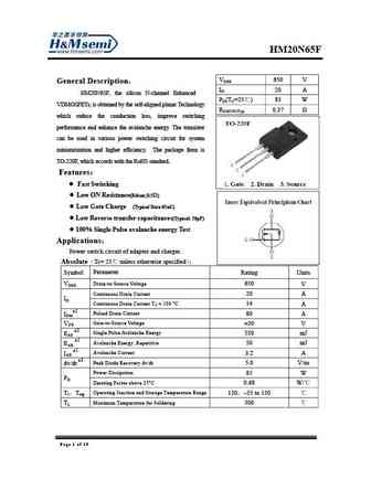
V General Description VDSS 650 ID 20 A HM20N65F, the silicon N-channel Enhanced PD(TC=25 ) 85 W VDMOSFETs, is obtained by the self-aligned planar Technology RDS(ON)Typ 0.37 which reduce the conduction loss, improve switching performance and enhance the avalanche energy. The transistor can be used in various power switching circuit for system miniaturizati
md20n65.pdf
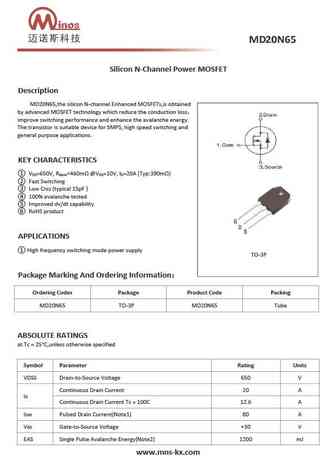
Silicon N-Channel Power MOSFET Description MD20N65,the silicon N-channel Enhanced MOSFETs,is obtained by advanced MOSFET technology which reduce the conduction loss improve switching performance and enhance the avalanche energy. The transistor is suitable device for SMPS, high speed switching and general purpose applications. KEY CHARACTERISTICS V =650V, R
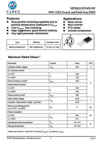
mpbq120n65gsf.pdf
MPBQ120N65GSF 650V-120A Trench and Field Stop IGBT Features Applications Easy parallel switching capability due to Motor drives positive temperature coefficient in VCEsat Main inverter Low VCEsat fast switching PTC heater High ruggedness, good thermal stability Climate Compressor Very tight parameter distribution Type Marking Package Code MPBQ120
mpbp20n65ef mpba20n65ef mpbc20n65ef mpbw20n65ef mpbt20n65ef.pdf
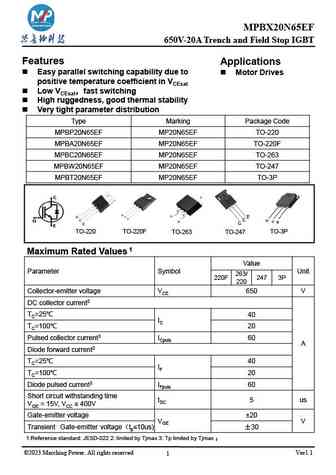
MPBX20N65EF 650V-20A Trench and Field Stop IGBT Features Applications Easy parallel switching capability due to Motor Drives positive temperature coefficient in VCEsat Low VCEsat fast switching High ruggedness, good thermal stability Very tight parameter distribution Type Marking Package Code MPBP20N65EF MP20N65EF TO-220 MPBA20N65EF MP20N65EF TO-220F MPBC20N6
mpva20n65f mpvp20n65f.pdf
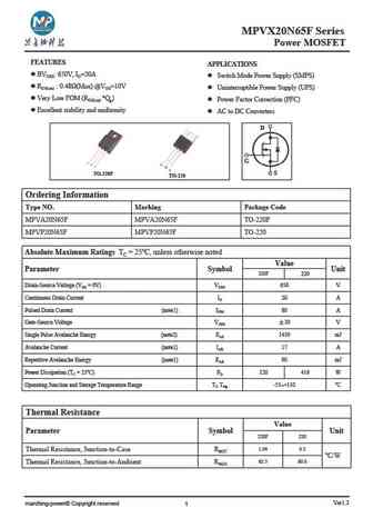
MPVX20N65F Series Power MOSFET MPSW60M041 FEATURES APPLICATIONS l BVDSS 650V, ID=20A l Switch Mode Power Supply (SMPS) l RDS(on) 0.48 (Max) @VGS=10V l Uninterruptible Power Supply (UPS) l Very Low FOM (RDS(on) *Qg) l Power Factor Correction (PFC) l Excellent stability and uniformity l AC to DC Converters D G TO-220F S TO-220 Ordering Information Type NO. Marking Package
ygf20n65t2 ygk20n65t2 ygp20n65t2 ygw20n65t2.pdf
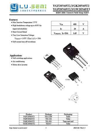
YGF20N65T2,YGK20N65T2 YGP20N65T2,YGW20N65T2 650V /20A Trench Field Stop IGBT Features Max Junction Temperature 175 C V 650 V CE High breakdown voltage up to 650V for improved reliability I 20 A C Short Circuit Rated V I =20A 1.65 V CE(SAT) C Very Low Saturation Voltage V = 1.65V (Typ.) @ I = 20A CE(SAT) C Soft current turn-off waveforms App
spa20n65c3.pdf
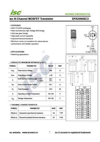
INCHANGE Semiconductor isc N-Channel MOSFET Transistor SPA20N65C3 FEATURES With TO-220F packaging New revolutionary high voltage technology Ultra low gate charge High peak current capability Improved transconductance Minimum Lot-to-Lot variations for robust device performance and reliable operation APPLICATIONS Switching applications ABSOLUTE MAXIMUM RATINGS(T =2
spp20n65c3.pdf
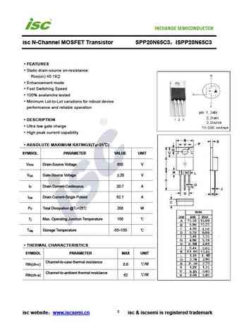
isc N-Channel MOSFET Transistor SPP20N65C3 ISPP20N65C3 FEATURES Static drain-source on-resistance RDS(on) 0.19 Enhancement mode Fast Switching Speed 100% avalanche tested Minimum Lot-to-Lot variations for robust device performance and reliable operation DESCRIPTION Ultra low gate charge High peak current capability ABSOLUTE MAXIMUM RATINGS(T =25 ) a
stp20n65m5.pdf
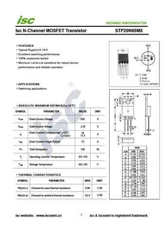
INCHANGE Semiconductor Isc N-Channel MOSFET Transistor STP20N65M5 FEATURES Typical R (on)=0.16 DS Excellent switching performance 100% avalanche tested Minimum Lot-to-Lot variations for robust device performance and reliable operation APPLICATIONS Switching applications ABSOLUTE MAXIMUM RATINGS(T =25 ) a SYMBOL PARAMETER VALUE UNIT V Drain-Source Voltage 650 V
20n65nf.pdf
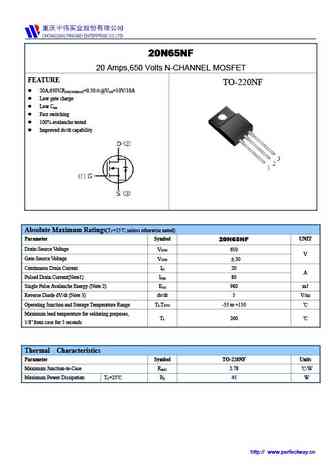
20N65NF 20 Amps,650 Volts N-CHANNEL MOSFET FEATURE TO-220NF 20A,650V,R =0.50 @V =10V/10A DS(ON)MAX GS Low gate charge Low C iss Fast switching 100% avalanche tested Improved dv/dt capability Absolute Maximum Ratings(T =25 ,unless otherwise noted) C Parameter Symbol UNIT 20N65NF Drain-Source Voltage V 650 DSS V Gate-Source Voltage V 30 GSS Contin
ap20n65f ap20n65p.pdf

AP20N65FIP 650V N-Channel Enhancement Mode MOSFET Description The AP20N65F/P is silicon N-channel Enhanced VDMOSFETs, is obtained by the self-aligned planar Technology which reduce the conduction loss, improve switching performance and enhance the avalanche energy. The transistor can be used in various power switching circuit for system miniaturization and higher efficiency.
Otros transistores... 7N65K, 8N65, 9N65, 10N65, 10N65Z, 10N65K, 15N65, 18N65, STF13NM60N, 22N65, 1N65A, 1N65, 2N65, 2N65L, 2N65Z, 2N65K, 3N65A
Parámetros del MOSFET. Cómo se afectan entre sí.
🌐 : EN ES РУ

Liste
Recientemente añadidas las descripciónes de los transistores:
MOSFET: BC2301 | BC1012W | BC1012T | BC1012 | 2SK3019WT | 2SK3019W | 2SK3018WT | CS95118 | CS85105A | CS75N45 | CS72N12 | CS55N50 | CS48N75A | CS40N27 | MSQ60P04D | MSQ40P07D
Popular searches
2sc1740 | c3229 | c2078 transistor | 2sc458 transistors | 2sa992 | 2sa970 | a970 | d2390 transistor