5N65 Datasheet. Equivalente. Reemplazo. Hoja de especificaciones. Principales características
Número de Parte: 5N65 📄📄
Tipo de FET: MOSFET
Polaridad de transistor: N
ESPECIFICACIONES MÁXIMAS
Pdⓘ - Máxima disipación de potencia: 100 W
|Vds|ⓘ - Voltaje máximo drenador-fuente: 650 V
|Vgs|ⓘ - Voltaje máximo fuente-puerta: 30 V
|Id|ⓘ - Corriente continua de drenaje: 5 A
Tjⓘ - Temperatura máxima de unión: 150 °C
CARACTERÍSTICAS ELÉCTRICAS
trⓘ - Tiempo de subida: 42 nS
Cossⓘ - Capacitancia de salida: 55 pF
RDSonⓘ - Resistencia estado encendido drenaje a fuente: 2 Ohm
📄📄 Copiar
Búsqueda de reemplazo de 5N65 MOSFET
- Selecciónⓘ de transistores por parámetros
5N65 datasheet
5n65.pdf
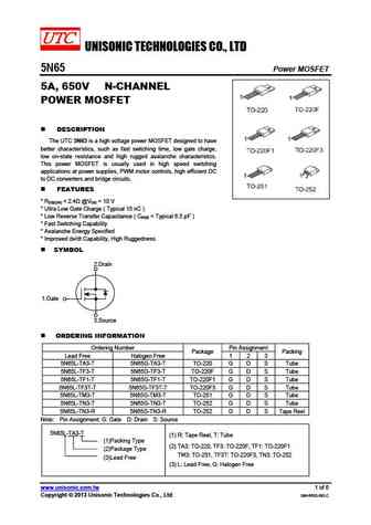
UNISONIC TECHNOLOGIES CO., LTD 5N65 Power MOSFET 5A, 650V N-CHANNEL POWER MOSFET DESCRIPTION The UTC 5N65 is a high voltage power MOSFET designed to have better characteristics, such as fast switching time, low gate charge, low on-state resistance and high rugged avalanche characteristics. This power MOSFET is usually used in high speed switching applications at power supp
5n65.pdf
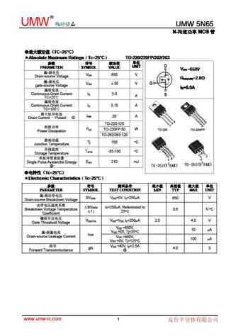
R UMW UMW 5N65 UMW 5N65 UMW 5N65 N- MOS N- MOS N- MOS N- MOS TC=25 C TC=25 C TC=25 C TC=25 C Absolute Maximum Ratings Tc=25 C TO-220/220FP/262/263 Absolute Maximum Ratings Tc=25 C TO-220/220FP/262/263 Absolute Maximum Ratings Tc=25 C TO-220/220FP/262/263 Absolute Maximum Ratings Tc=25 C TO-220/220FP/
5n65 5n65f 5n65d 5n65e 5n65m 5n65n.pdf
R 5N65 5N65F 5N65D 5N65E 5N65M 5N65N S E M I C O N D U C T O R 650V N-Channel Power MOSFET FEATURES PRODUCT SUMMARY RDS(ON)
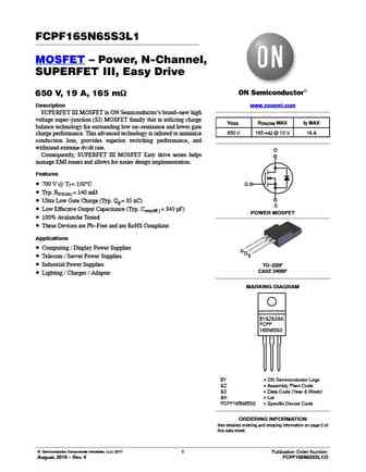
fcpf165n65s3l1.pdf
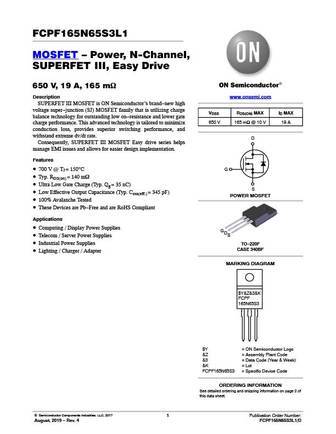
FCPF165N65S3L1 MOSFET Power, N-Channel, SUPERFET III, Easy Drive 650 V, 19 A, 165 mW Description www.onsemi.com SUPERFET III MOSFET is ON Semiconductor s brand-new high voltage super-junction (SJ) MOSFET family that is utilizing charge VDSS RDS(ON) MAX ID MAX balance technology for outstanding low on-resistance and lower gate 650 V 165 mW @ 10 V 19 A charge performance. This adv
swd5n65k.pdf
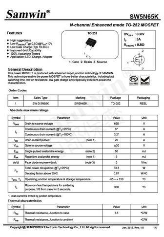
SW5N65K N-channel Enhanced mode TO-252 MOSFET Features TO-252 BVDSS 650V ID 5A High ruggedness Low RDS(ON) (Typ 0.8 )@VGS=10V RDS(ON) 0.8 Low Gate Charge (Typ 10.3nC) Improved dv/dt Capability 2 100% Avalanche Tested 1 2 Application LED, Charge, Adaptor 3 1. Gate 2. Drain 3. Source 1 3 General Description This power MOSFE
irfib5n65a.pdf
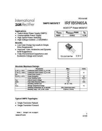
PD-91816B SMPS MOSFET IRFIB5N65A HEXFET Power MOSFET Applications VDSS RDS(on) max ID Switch Mode Power Supply (SMPS) Uninterruptible Power Supply 650V 0.93 5.1A High Speed Power Switching High Voltage Isolation = 2.5KVRMS Benefits Low Gate Charge Qg results in Simple Drive Requirement Improved Gate, Avalanche and Dynamic dv/dt Ruggedness Fully Characterized Capacita
irfib5n65apbf.pdf
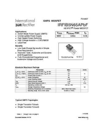
PD-94837 SMPS MOSFET IRFIB5N65APbF HEXFET Power MOSFET Applications VDSS RDS(on) max ID l Switch Mode Power Supply (SMPS) l Uninterruptible Power Supply 650V 0.93 5.1A l High Speed Power Switching l High Voltage Isolation = 2.5KVRMS l Lead-Free Benefits l Low Gate Charge Qg results in Simple Drive Requirement l Improved Gate, Avalanche and Dynamic dv/dt Ruggedness G D S
ste145n65m5.pdf
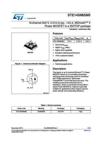
STE145N65M5 N-channel 650 V, 0.012 typ., 143 A, MDmesh V Power MOSFET in a ISOTOP package Datasheet - preliminary data Features Order code VDS @Tjmax RDS(on) max ID STE145N65M5 710 V 0.015 143 A Very low RDS(on) Higher VDSS rating Higher dv/dt capability ISOTOP Excellent switching performance 100% avalanche tested Applications Figure 1. Internal sch
stw35n65dm2.pdf
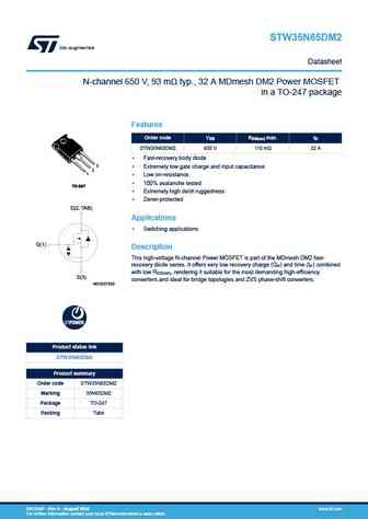
STW35N65DM2 Datasheet N-channel 650 V, 93 m typ., 32 A MDmesh DM2 Power MOSFET in a TO-247 package Features VDS RDS(on) max. ID Order code STW35N65DM2 650 V 110 m 32 A Fast-recovery body diode 3 Extremely low gate charge and input capacitance 2 1 Low on-resistance 100% avalanche tested TO-247 Extremely high dv/dt ruggedness Zener-protected D(2, TAB
stfw45n65m5 stwa45n65m5.pdf
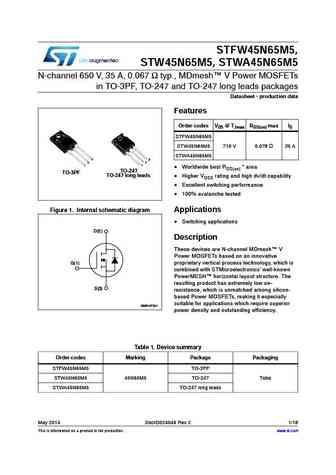
STFW45N65M5, STW45N65M5, STWA45N65M5 N-channel 650 V, 35 A, 0.067 typ., MDmesh V Power MOSFETs in TO-3PF, TO-247 and TO-247 long leads packages Datasheet - production data Features Order codes VDS @ TJmax RDS(on) max ID STFW45N65M5 STW45N65M5 710 V 0.078 35 A 1 1 1 STWA45N65M5 3 3 2 2 1 1 Worldwide best RDS(on) * area TO-247 TO-3PF TO-247 long leads Hig
stw65n65dm2ag.pdf
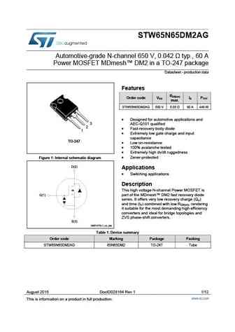
STW65N65DM2AG Automotive-grade N-channel 650 V, 0.042 typ., 60 A Power MOSFET MDmesh DM2 in a TO-247 package Datasheet - production data Features R DS(on) Order code V I P DS D TOT max. STW65N65DM2AG 650 V 0.05 60 A 446 W Designed for automotive applications and 3 AEC-Q101 qualified 2 Fast-recovery body diode 1 Extremely low gate charge and inpu
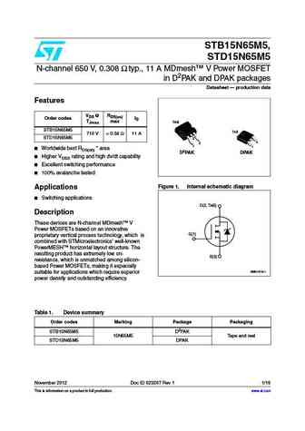
stb15n65m5 std15n65m5.pdf
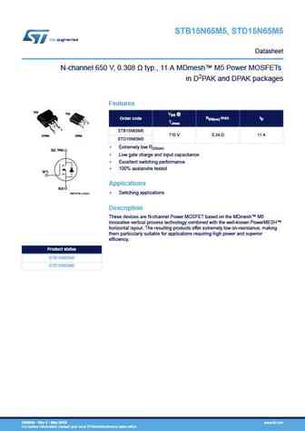
STB15N65M5, STD15N65M5 Datasheet N-channel 650 V, 0.308 typ., 11 A MDmesh M5 Power MOSFETs in D2PAK and DPAK packages Features TAB TAB VDS @ RDS(on) max. ID Order code TJmax 3 2 2 1 3 STB15N65M5 1 710 V 0.34 11 A D2PAK DPAK STD15N65M5 Extremely low RDS(on) D(2, TAB) Low gate charge and input capacitance Excellent switching performance 100% aval
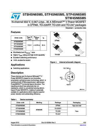
stb45n65m5 stf45n65m5 stp45n65m5.pdf
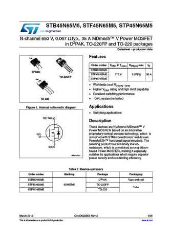
STB45N65M5, STF45N65M5, STP45N65M5 N-channel 650 V, 0.067 typ., 35 A MDmesh V Power MOSFET in D2PAK, TO-220FP and TO-220 packages Datasheet - production data Features TAB 2 Order codes VDSS @ TJmax RDS(on) max ID 3 1 STB45N65M5 3 2 D2PAK 1 STF45N65M5 710 V 0.078 35 A TO-220FP STP45N65M5 TAB Worldwide best RDS(on) * area Higher VDSS rating and high dv/dt capa
stfw45n65m5 stw45n65m5 stwa45n65m5.pdf

STFW45N65M5, STW45N65M5, STWA45N65M5 N-channel 650 V, 35 A, 0.067 typ., MDmesh V Power MOSFETs in TO-3PF, TO-247 and TO-247 long leads packages Datasheet - production data Features Order codes VDS @ TJmax RDS(on) max ID STFW45N65M5 STW45N65M5 710 V 0.078 35 A 1 1 1 STWA45N65M5 3 3 2 2 1 1 Worldwide best RDS(on) * area TO-247 TO-3PF TO-247 long leads Hig
stb35n65m5 stf35n65m5 sti35n65m5 stp35n65m5 stw35n65m5.pdf
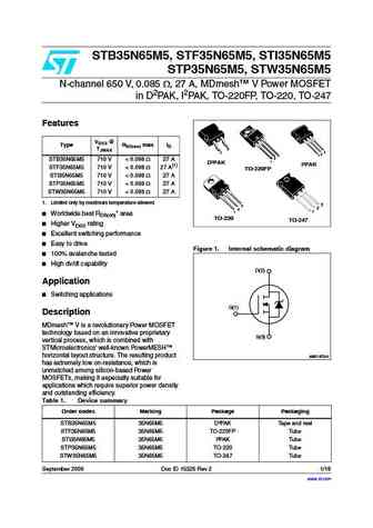
STB35N65M5, STF35N65M5, STI35N65M5 STP35N65M5, STW35N65M5 N-channel 650 V, 0.085 , 27 A, MDmesh V Power MOSFET in D2PAK, I2PAK, TO-220FP, TO-220, TO-247 Features VDSS @ Type RDS(on) max ID TJMAX 3 3 1 2 3 1 2 STB35N65M5 710 V
stb45n65m5 stf45n65m5 stp45n65m5 stw45n65m5.pdf
STB45N65M5, STF45N65M5, STP45N65M5 STW45N65M5 N-channel 650 V, 0.067 typ., 35 A MDmesh V Power MOSFET in D2PAK, TO-220FP, TO-220 and TO-247 packages Datasheet production data Features TAB 2 VDSS @ RDS(on) 3 Order code ID 1 TJmax max 3 2 D2PAK 1 STB45N65M5 TO-220FP TAB STF45N65M5 710 V
sty145n65m5.pdf
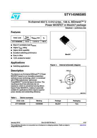
STY145N65M5 N-channel 650 V, 0.012 typ., 138 A, MDmesh V Power MOSFET in Max247 package Datasheet preliminary data Features VDSS Order code @TJmax RDS(on) max ID STY145N65M5 710 V
std15n65m5.pdf
STB15N65M5, STD15N65M5 N-channel 650 V, 0.308 typ., 11 A MDmesh V Power MOSFET in D2PAK and DPAK packages Datasheet production data Features VDS @ RDS(on) Order codes ID TJmax max TAB STB15N65M5 TAB 710 V
stb15n65.pdf
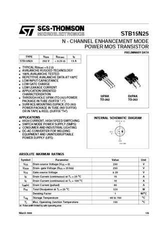
STB15N25 N - CHANNEL ENHANCEMENT MODE POWER MOS TRANSISTOR PRELIMINARY DATA TYPE V R I DSS DS(on) D STB15N25 250 V
stf15n65m5 stfi15n65m5 stp15n65m5.pdf
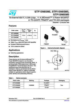
STF15N65M5, STFI15N65M5, STP15N65M5 N-channel 650 V, 0.308 typ., 11 A MDmesh V Power MOSFET in TO-220FP, I2PAKFP and TO-220 packages Datasheet production data Features VDS @ RDS(on) Order codes ID TJmax max 3 2 1 STF15N65M5 TO-220FP STFI15N65M5 710 V
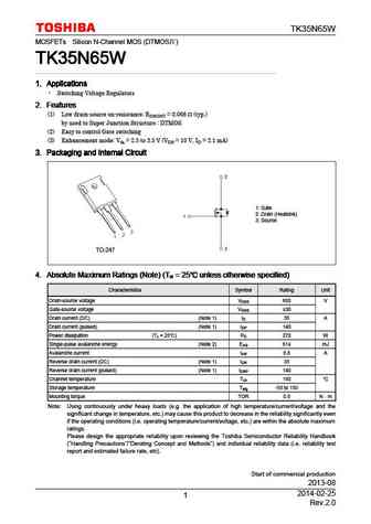
tk35n65w5.pdf

TK35N65W5 MOSFETs Silicon N-Channel MOS (DTMOS ) TK35N65W5 TK35N65W5 TK35N65W5 TK35N65W5 1. Applications 1. Applications 1. Applications 1. Applications Switching Voltage Regulators 2. Features 2. Features 2. Features 2. Features (1) Fast reverse recovery time trr = 130 ns (typ.) (2) Low drain-source on-resistance RDS(ON) = 0.08 (typ.) by used to Super Junction Str
tk35n65w.pdf
TK35N65W MOSFETs Silicon N-Channel MOS (DTMOS ) TK35N65W TK35N65W TK35N65W TK35N65W 1. Applications 1. Applications 1. Applications 1. Applications Switching Voltage Regulators 2. Features 2. Features 2. Features 2. Features (1) Low drain-source on-resistance RDS(ON) = 0.068 (typ.) by used to Super Junction Structure DTMOS (2) Easy to control Gate switching (3) E
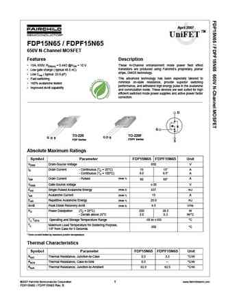
fdp15n65 fdpf15n65.pdf

April 2007 TM UniFET FDP15N65 / FDPF15N65 650V N-Channel MOSFET Features Description 15A, 650V, RDS(on) = 0.44 @VGS = 10 V These N-Channel enhancement mode power field effect transistors are produced using Fairchild s proprietary, planar Low gate charge ( typical 48.5 nC) stripe, DMOS technology. Low Crss ( typical 23.6 pF) This advanced technology has been especia
fda15n65.pdf
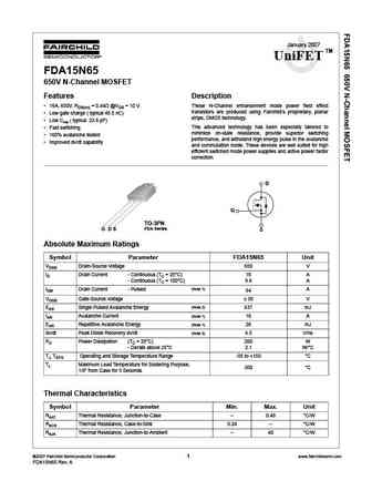
January 2007 TM UniFET FDA15N65 650V N-Channel MOSFET Features Description 16A, 650V, RDS(on) = 0.44 @VGS = 10 V These N-Channel enhancement mode power field effect transistors are produced using Fairchild s proprietary, planar Low gate charge ( typical 48.5 nC) stripe, DMOS technology. Low Crss ( typical 23.6 pF) This advanced technology has been especially tailor
fdp15n65 fdpf15n65ydtu.pdf
April 2007 TM UniFET FDP15N65 / FDPF15N65 650V N-Channel MOSFET Features Description 15A, 650V, RDS(on) = 0.44 @VGS = 10 V These N-Channel enhancement mode power field effect transistors are produced using Fairchild s proprietary, planar Low gate charge ( typical 48.5 nC) stripe, DMOS technology. Low Crss ( typical 23.6 pF) This advanced technology has been especia
sihf15n65e.pdf
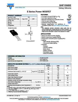
SiHF15N65E www.vishay.com Vishay Siliconix E Series Power MOSFET FEATURES PRODUCT SUMMARY Low figure-of-merit (FOM) Ron x Qg VDS (V) at TJ max. 700 Available Low input capacitance (Ciss) RDS(on) max. at 25 C ( ) VGS = 10 V 0.28 Reduced switching and conduction losses Available Qg max. (nC) 96 Ultra low gate charge (Qg) Qgs (nC) 11 Avalanche energy rated (U
sihfib5n65a.pdf

IRFIB5N65A, SiHFIB5N65A Vishay Siliconix Power MOSFET FEATURES PRODUCT SUMMARY Low Gate Charge Qg Results in Simple Drive VDS (V) 650 Available Requirement RDS(on) ( )VGS = 10 V 0.93 RoHS* Improved Gate, Avalanche and Dynamic dV/dt COMPLIANT Qg (Max.) (nC) 48 Ruggedness Qgs (nC) 12 Fully Characterized Capacitance and Avalanche Voltage and Current Qgd (nC) 19
sihp15n65e.pdf
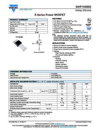
SiHP15N65E www.vishay.com Vishay Siliconix E Series Power MOSFET FEATURES PRODUCT SUMMARY Low figure-of-merit (FOM) Ron x Qg VDS (V) at TJ max. 700 Available Low input capacitance (Ciss) RDS(on) max. at 25 C ( ) VGS = 10 V 0.28 Reduced switching and conduction losses Available Qg max. (nC) 96 Ultra low gate charge (Qg) Qgs (nC) 11 Avalanche energy rated (U
sihb15n65e.pdf
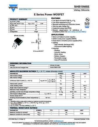
SiHB15N65E www.vishay.com Vishay Siliconix E Series Power MOSFET FEATURES PRODUCT SUMMARY Low figure-of-merit (FOM) Ron x Qg VDS (V) at TJ max. 700 Low input capacitance (Ciss) RDS(on) max. at 25 C ( ) VGS = 10 V 0.28 Reduced switching and conduction losses Qg max. (nC) 96 Ultra low gate charge (Qg) Qgs (nC) 11 Avalanche energy rated (UIS) Qgd (nC) 21
irfib5n65a sihfib5n65a.pdf
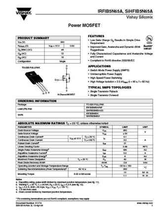
IRFIB5N65A, SiHFIB5N65A Vishay Siliconix Power MOSFET FEATURES PRODUCT SUMMARY Low Gate Charge Qg Results in Simple Drive VDS (V) 650 Available Requirement RDS(on) ( )VGS = 10 V 0.93 RoHS* Improved Gate, Avalanche and Dynamic dV/dt COMPLIANT Qg (Max.) (nC) 48 Ruggedness Qgs (nC) 12 Fully Characterized Capacitance and Avalanche Voltage and Current Qgd (nC) 19
ikz75n65el5.pdf

IGBT Low V IGBT in TRENCHSTOPTM 5 technology copacked with RAPID 1 CE(sat) fast and soft antiparallel diode IKZ75N65EL5 650V DuoPack IGBT and diode Low V series fifth generation CE(sat) Data sheet Industrial Power Control IKZ75N65EL5 Low V series fifth generation CE(sat) Low V IGBT in TRENCHSTOPTM 5 technology copacked with RAPID 1 CE(sat) fast and soft antiparallel diode Featu
ikw75n65eh5.pdf
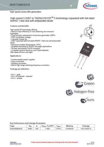
IKW75N65EH5 High speed series fifth generation High speed 5 IGBT in TRENCHSTOPTM 5 technology copacked with full-rated RAPID 1 fast and soft antiparallel diode C Features and Benefits High speed H5 technology offering Best-in-Class efficiency in hard switching and resonant topologies Plug and play replacement of previous generation IGBTs G 650V breakdown voltage E
igw75n65h5.pdf

IGW75N65H5 High speed series fifth generation High speed 5 IGBT in TRENCHSTOPTM 5 technology Features and Benefits C High speed H5 technology offering Best-in-Class efficiency in hard switching and resonant topologies Plug and play replacement of previous generation IGBTs 650V breakdown voltage G Low Q E G Maximum junction temperature 175 C Qualified accord
ikz75n65es5.pdf
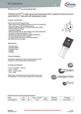
IKZ75N65ES5 TRENCHSTOPTM 5 soft switching IGBT TRENCHSTOPTM 5 high speed soft switching IGBT copacked with full current rated RAPID 1 fast and soft antiparallel diode Features and Benefits High speed S5 technology offering High speed smooth switching device for hard & soft switching Very Low V , 1.42V at nominal current CEsat Plug and play replacement of previous generatio
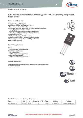
ika15n65h5.pdf

IGBT High speed 5 IGBT in TRENCHSTOPTM 5 technology copacked with RAPID 1 fast and soft antiparallel diode IKA15N65H5 650V DuoPack IGBT and Diode High speed switching series fifth generation Data sheet Industrial Power Control IKA15N65H5 High speed switching series fifth generation High speed 5 IGBT in TRENCHSTOPTM 5 technology copacked with RAPID 1 fast and soft antiparallel diode
ikp15n65f5.pdf
IGBT High speed 5 FAST IGBT in TRENCHSTOPTM 5 technology copacked with RAPID 1 fast and soft antiparallel diode IKP15N65F5 650V DuoPack IGBT and Diode High speed switching series fifth generation Data sheet Industrial Power Control IKP15N65F5 High speed switching series fifth generation High speed 5 FAST IGBT in TRENCHSTOPTM 5 technology copacked with RAPID 1 fast and soft antiparal
ikz75n65eh5.pdf
IGBT High speed 5 IGBT in TRENCHSTOPTM 5 technology copacked with RAPID 1 fast and soft antiparallel diode IKZ75N65EH5 650V DuoPack IGBT and diode High speed series fifth generation Data sheet Industrial Power Control IKZ75N65EH5 High speed series fifth generation High speed 5 IGBT in TRENCHSTOPTM 5 technology copacked with RAPID 1 fast and soft antiparallel diode Features and Bene
ika15n65et6.pdf
IKA15N65ET6 TRENCHSTOP IGBT6 IGBT in trench and field-stop technology with soft, fast recovery anti-parallel Rapid diode C Features and Benefits Very low V 1.5V (typ.) CE(sat) Maximum junction temperature 175 C Short circuit withstand time 3 s Trench and field-stop technology for 650V applications offers G very tight parameter distribution E high rugg
ikb15n65eh5.pdf
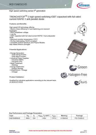
IKB15N65EH5 High speed switching series 5th generation TRENCHSTOPTM 5 high speed switching IGBT copacked with full rated current RAPID 1 anti parallel diode C Features and Benefits High speed H5 technology offering Best-in-Class efficiency in hard switching and resonant topologies 650V breakdown voltage G Low Q G E IGBT copacked with full rated current RAPID 1 fas
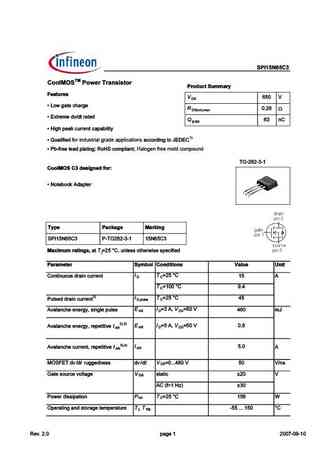
spa15n65c3.pdf
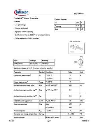
SPA15N65C3 CoolMOSTM Power Transistor Product Summary Features V 650 V DS Low gate charge R 0.28 DS(on),max Extreme dv/dt rated Q 63 nC g,typ High peak current capability Qualified according to JEDEC1) for target applications Pb-free lead plating; RoHS compliant PG-TO220-3-31 Type Package Marking SPA15N65C3 PG-TO220-3-31 15N65C3 Maximum ratings, at T =
spi15n65c3.pdf
SPI15N65C3 C IMOSTM $;B1= '=- >5>?;= $=;0@/? &@99-=D Features 650 V DS R 'AH 93E7 5 3C97 0.28 W DS(on) max R IEC7?7 6G 6E C3E76 6 nC g typ R #;9 B73= 5FCC7@E 53B34;>;EJ R , F3>;8;76 for industrial grade applications 355AC6;@9 EA % R +4 8C77 >736 B>3E;@9 - A#. 5A?B>;3@E; Halogen free mold compound TO 262 1 ;;8!#& 01>53 10 2;= R ) AE74AA= 63BE7C Type Package Mar
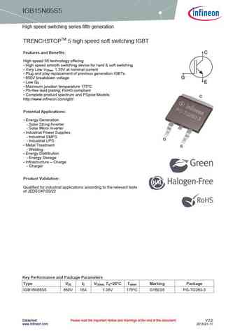
igb15n65s5.pdf
IGB15N65S5 High speed switching series fifth generation TRENCHSTOPTM 5 high speed soft switching IGBT Features and Benefits C High speed S5 technology offering High speed smooth switching device for hard & soft switching Very Low V , 1.35V at nominal current CEsat Plug and play replacement of previous generation IGBTs 650V breakdown voltage G Low Q E G Maxim
igz75n65h5.pdf
IGBT High speed 5 IGBT in TRENCHSTOPTM 5 technology IGZ75N65H5 650V IGBT high speed series fifth generation Data sheet Industrial Power Control IGZ75N65H5 High speed series fifth generation High speed 5 IGBT in TRENCHSTOPTM 5 technology Features and Benefits High speed H5 technology offering Ultra low loss switching thanks to Kelvin emitter pin in combination with TRENCHSTOPTM
ikw75n65el5.pdf

IGBT Low V IGBT in TRENCHSTOPTM 5 technology copacked with RAPID 1 CE(sat) fast and soft antiparallel diode IKW75N65EL5 650V DuoPack IGBT and diode Low V series fifth generation CE(sat) Data sheet Industrial Power Control IKW75N65EL5 Low V series fifth generation CE(sat) Low V IGBT in TRENCHSTOPTM 5 technology copacked with RAPID 1 CE(sat) fast and soft antiparallel diode C Fe
spp15n65c3.pdf
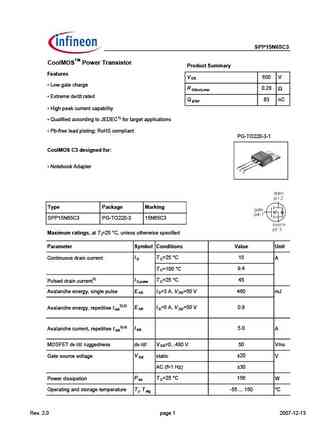
SPP15N65C3 CoolMOSTM Power Transistor Product Summary Features V 650 V DS Low gate charge R 0.28 DS(on),max Extreme dv/dt rated Q 63 nC g,typ High peak current capability Qualified according to JEDEC1) for target applications Pb-free lead plating; RoHS compliant PG-TO220-3-1 CoolMOS C3 designed for Notebook Adapter Type Package Marking SPP15N65C3
ika15n65f5.pdf

IGBT High speed 5 FAST IGBT in TRENCHSTOPTM 5 technology copacked with RAPID 1 fast and soft antiparallel diode IKA15N65F5 650V DuoPack IGBT and Diode High speed switching series fifth generation Data sheet Industrial Power Control IKA15N65F5 High speed switching series fifth generation High speed 5 FAST IGBT in TRENCHSTOPTM 5 technology copacked with RAPID 1 fast and soft antiparal
ikp15n65h5.pdf

IGBT High speed 5 IGBT in TRENCHSTOPTM technology copacked with RAPID 1 fast and soft antiparallel diode IKP15N65H5 650V DuoPack IGBT and Diode High speed switching series fifth generation Data sheet Industrial Power Control IKP15N65H5 High speed switching series fifth generation High speed 5 IGBT in TRENCHSTOPTM technology copacked with RAPID 1 fast and soft antiparallel diode C
ikw75n65es5.pdf
IGBT TRENCHSTOPTM 5 high Speed soft switching IGBT with full current rated RAPID 1 diode IKW75N65ES5 650V TRENCHSTOPTM 5 high speed soft switching duopak Data sheet Industrial Power Control IKW75N65ES5 TRENCHSTOPTM 5 soft switching IGBT TRENCHSTOPTM 5 high speed soft switching IGBT copacked with full current rated RAPID 1 fast and soft antiparallel diode C Features and Benefits Hi
ixyp15n65c3d1.pdf

Preliminary Technical Information XPTTM 650V IGBT VCES = 650V IXYA15N65C3D1 GenX3TM w/Diode IC110 = 15A IXYP15N65C3D1 VCE(sat) 2.5V tfi(typ) = 28ns Extreme Light Punch Through IGBT for 20-60kHz Switching TO-263 AA (IXYA) G Symbol Test Conditions Maximum Ratings E C (Tab) VCES TJ = 25 C to 175 C 650 V VCGR
ixyh75n65c3h1.pdf

Preliminary Technical Information VCES = 650V XPTTM 650V IGBT IXYH75N65C3H1 IC110 = 75A GenX3TM w/ Sonic VCE(sat) 2.3V Diode tfi(typ) = 50ns Extreme Light Punch through IGBT for 20-60kHz Switching TO-247 AD Symbol Test Conditions Maximum Ratings VCES TJ = 25 C to 175 C 650 V VCGR TJ = 25 C to 175 C, RGE =
ixyn75n65c3d1.pdf
Advance Technical Information VCES = 650V XPTTM 650V IGBT IXYN75N65C3D1 IC110 = 75A GenX3TM w/ Diode VCE(sat) 2.3V tfi(typ) = 60ns Extreme Light Punch through IGBT for 20-60kHz Switching E SOT-227B, miniBLOC E153432 Symbol Test Conditions Maximum Ratings E VCES TJ = 25 C to 175 C 650 V G VCGR TJ = 25
ixyp15n65c3.pdf
Preliminary Technical Information XPTTM 650V IGBT VCES = 650V IXYP15N65C3 GenX3TM IC110 = 15A VCE(sat) 2.5V tfi(typ) = 28ns Extreme Light Punch Through IGBT for 20-60kHz Switching TO-220 Symbol Test Conditions Maximum Ratings VCES TJ = 25 C to 175 C 650 V VCGR TJ = 25 C to 175 C, RGE = 1M 650 V G C Tab
ixyp15n65c3d1m.pdf
Preliminary Technical Information XPTTM 650V IGBT VCES = 650V IXYP15N65C3D1M GenX3TM w/Diode IC110 = 9A VCE(sat) 2.5V (Electrically Isolated Tab) tfi(typ) = 28ns Extreme Light Punch Through IGBT for 20-60kHz Switching OVERMOLDED TO-220 Symbol Test Conditions Maximum Ratings VCES TJ = 25 C to 175 C 650 V VCGR
ixya15n65c3d1.pdf
Preliminary Technical Information XPTTM 650V IGBT VCES = 650V IXYA15N65C3D1 GenX3TM w/Diode IC110 = 15A IXYP15N65C3D1 VCE(sat) 2.5V tfi(typ) = 28ns Extreme Light Punch Through IGBT for 20-60kHz Switching TO-263 AA (IXYA) G Symbol Test Conditions Maximum Ratings E C (Tab) VCES TJ = 25 C to 175 C 650 V VCGR
ixyh75n65c3d1.pdf
Preliminary Technical Information VCES = 650V XPTTM 650V IGBT IXYH75N65C3D1 IC110 = 75A GenX3TM w/ Diode VCE(sat) 2.3V tfi(typ) = 60ns Extreme Light Punch through IGBT for 20-60kHz Switching TO-247 AD Symbol Test Conditions Maximum Ratings VCES TJ = 25 C to 175 C 650 V VCGR TJ = 25 C to 175 C, RGE = 1M 6
ixyh75n65c3.pdf
VCES = 650V XPTTM 650V IGBT IXYH75N65C3 IC110 = 75A GenX3TM VCE(sat) 2.3V tfi(typ) = 60ns Extreme Light Punch through IGBT for 20-60kHz Switching TO-247AD Symbol Test Conditions Maximum Ratings VCES TJ = 25 C to 175 C 650 V VCGR TJ = 25 C to 175 C, RGE = 1M 650 V VGES Continuous 20 V G C Tab VGEM
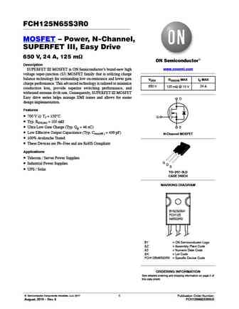
fcp125n65s3r0.pdf
FCP125N65S3R0 MOSFET Power, N-Channel, SUPERFET) III, Easy Drive 650 V, 24 A, 125 mW Description www.onsemi.com SUPERFET III MOSFET is ON Semiconductor s brand-new high voltage super-junction (SJ) MOSFET family that is utilizing charge balance technology for outstanding low on-resistance and lower gate VDSS RDS(ON) MAX ID MAX charge performance. This advanced technology is tailo
fchd125n65s3r0.pdf
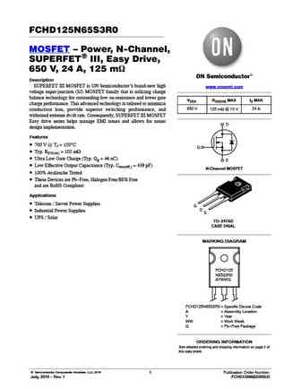
FCHD125N65S3R0 MOSFET Power, N-Channel, SUPERFET) III, Easy Drive, 650 V, 24 A, 125 mW Description SUPERFET III MOSFET is ON Semiconductor s brand-new high www.onsemi.com voltage super-junction (SJ) MOSFET family that is utilizing charge balance technology for outstanding low on-resistance and lower gate VDSS RDS(ON) MAX ID MAX charge performance. This advanced technology is tai
fcpf165n65s3r0l.pdf
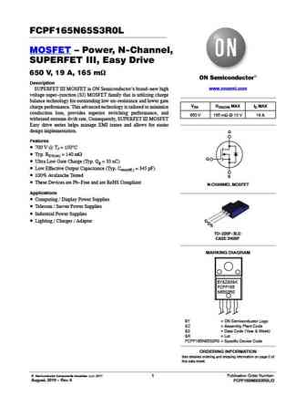
FCPF165N65S3R0L MOSFET Power, N-Channel, SUPERFET III, Easy Drive 650 V, 19 A, 165 mW Description www.onsemi.com SUPERFET III MOSFET is ON Semiconductor s brand-new high voltage super-junction (SJ) MOSFET family that is utilizing charge balance technology for outstanding low on-resistance and lower gate VDS RDS(ON) MAX ID MAX charge performance. This advanced technology is tailo
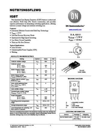
ngtb35n65fl2.pdf
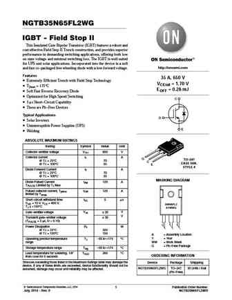
NGTB35N65FL2WG IGBT - Field Stop II This Insulated Gate Bipolar Transistor (IGBT) features a robust and cost effective Field Stop II Trench construction, and provides superior performance in demanding switching applications, offering both low on state voltage and minimal switching loss. The IGBT is well suited for UPS and solar applications. Incorporated into the device is a soft http //
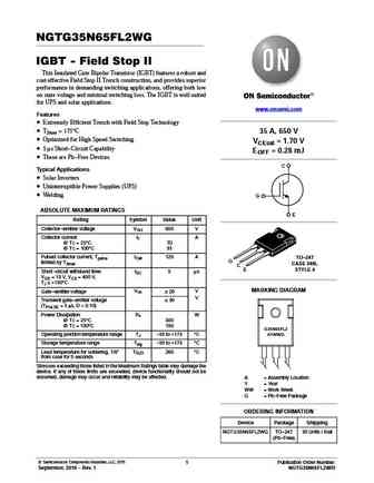
ngtg35n65fl2.pdf
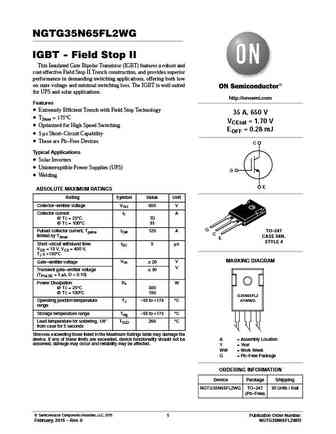
NGTG35N65FL2WG IGBT - Field Stop II This Insulated Gate Bipolar Transistor (IGBT) features a robust and cost effective Field Stop II Trench construction, and provides superior performance in demanding switching applications, offering both low on state voltage and minimal switching loss. The IGBT is well suited for UPS and solar applications. http //onsemi.com Features Extremely Eff
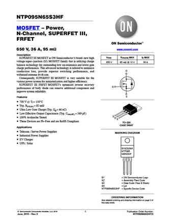
ntb095n65s3hf.pdf
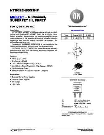
NTB095N65S3HF MOSFET N Channel, SUPERFET III, FRFET 650 V, 36 A, 95 mW Description www.onsemi.com SUPERFET III MOSFET is ON Semiconductor s brand-new high voltage super-junction (SJ) MOSFET family that is utilizing charge VDSS RDS(ON) MAX ID MAX balance technology for outstanding low on-resistance and lower gate 650 V 95 mW @ 10 V 36 A charge performance. This advanced technol
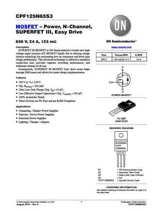
fcp125n65s3.pdf
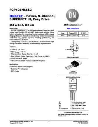
FCP125N65S3 MOSFET Power, N-Channel, SUPERFET III, Easy Drive 650 V, 24 A, 125 mW Description www.onsemi.com SUPERFET III MOSFET is ON Semiconductor s brand-new high voltage super-junction (SJ) MOSFET family that is utilizing charge VDSS RDS(ON) MAX ID MAX balance technology for outstanding low on-resistance and lower gate 650 V 125 mW @ 10 V 24 A charge performance. This advanc
nthl095n65s3hf.pdf
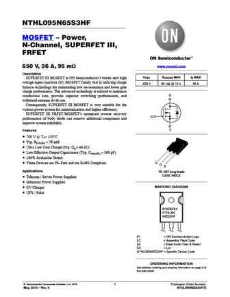
NTHL095N65S3HF MOSFET Power, N Channel, SUPERFET III, FRFET www.onsemi.com 650 V, 36 A, 95 mW Description VDSS RDS(ON) MAX ID MAX SUPERFET III MOSFET is ON Semiconductor s brand-new high voltage super-junction (SJ) MOSFET family that is utilizing charge 650 V 95 mW @ 10 V 36 A balance technology for outstanding low on-resistance and lower gate charge performance. This advanc
ntp055n65s3h.pdf
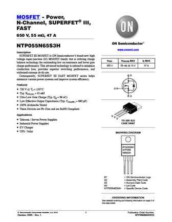
MOSFET - Power, N Channel, SUPERFET) III, FAST 650 V, 55 mW, 47 A NTP055N65S3H www.onsemi.com Description SUPERFET III MOSFET is ON Semiconductor s brand-new high voltage super-junction (SJ) MOSFET family that is utilizing charge VDSS RDS(ON) MAX ID MAX balance technology for outstanding low on-resistance and lower gate 650 V 55 mW @ 10 V 47 A charge performance. This advanced t
fdp15n65 fdpf15n65.pdf

April 2007 TM UniFET FDP15N65 / FDPF15N65 650V N-Channel MOSFET Features Description 15A, 650V, RDS(on) = 0.44 @VGS = 10 V These N-Channel enhancement mode power field effect transistors are produced using Fairchild s proprietary, planar Low gate charge ( typical 48.5 nC) stripe, DMOS technology. Low Crss ( typical 23.6 pF) This advanced technology has been especia
ngtg35n65fl2wg.pdf
NGTG35N65FL2WG IGBT - Field Stop II This Insulated Gate Bipolar Transistor (IGBT) features a robust and cost effective Field Stop II Trench construction, and provides superior performance in demanding switching applications, offering both low on state voltage and minimal switching loss. The IGBT is well suited for UPS and solar applications. www.onsemi.com Features Extremely Effici
ngtb75n65fl2.pdf
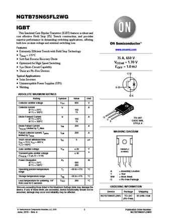
NGTB75N65FL2WG IGBT This Insulated Gate Bipolar Transistor (IGBT) features a robust and cost effective Field Stop (FS) Trench construction, and provides superior performance in demanding switching applications, offering both low on state voltage and minimal switching loss. Features www.onsemi.com Extremely Efficient Trench with Field Stop Technology TJmax = 175 C 75 A, 650 V
ngtb35n65fl2wg.pdf
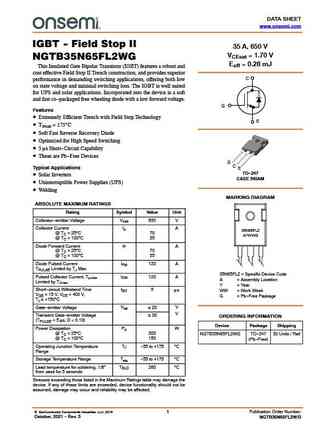
DATA SHEET www.onsemi.com IGBT - Field Stop II 35 A, 650 V VCEsat = 1.70 V NGTB35N65FL2WG Eoff = 0.28 mJ This Insulated Gate Bipolar Transistor (IGBT) features a robust and cost effective Field Stop II Trench construction, and provides superior C performance in demanding switching applications, offering both low on state voltage and minimal switching loss. The IGBT is well suited fo
fch125n65s3r0.pdf
FCH125N65S3R0 MOSFET Power, N-Channel, SUPERFET III, Easy Drive 650 V, 24 A, 125 mW Description www.onsemi.com SUPERFET III MOSFET is ON Semiconductor s brand-new high voltage super-junction (SJ) MOSFET family that is utilizing charge balance technology for outstanding low on-resistance and lower gate VDSS RDS(ON) MAX ID MAX charge performance. This advanced technology is tailor
fcb125n65s3.pdf
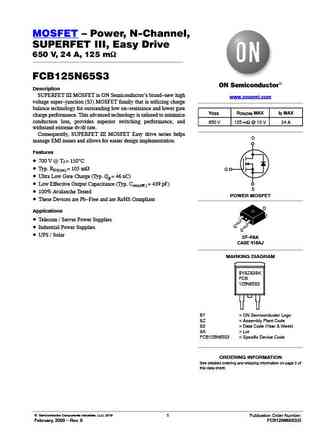
MOSFET Power, N-Channel, SUPERFET III, Easy Drive 650 V, 24 A, 125 mW FCB125N65S3 Description SUPERFET III MOSFET is ON Semiconductor s brand-new high www.onsemi.com voltage super-junction (SJ) MOSFET family that is utilizing charge balance technology for outstanding low on-resistance and lower gate VDSS RDS(ON) MAX ID MAX charge performance. This advanced technology is tailored
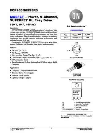
fcp165n65s3.pdf

FCP165N65S3 MOSFET Power, N-Channel, SUPERFET III, Easy-Drive 650 V, 19 A, 165 mW Description www.onsemi.com SUPERFET III MOSFET is ON Semiconductor s brand-new high voltage super-junction (SJ) MOSFET family that is utilizing charge VDSS RDS(ON) MAX ID MAX balance technology for outstanding low on-resistance and lower gate 650 V 165 mW @ 10 V 19 A charge performance. This advanc
ngtb75n65fl2wg.pdf
NGTB75N65FL2WG IGBT This Insulated Gate Bipolar Transistor (IGBT) features a robust and cost effective Field Stop (FS) Trench construction, and provides superior performance in demanding switching applications, offering both low on state voltage and minimal switching loss. Features www.onsemi.com Extremely Efficient Trench with Field Stop Technology TJmax = 175 C 75 A, 650 V
fcp165n65s3r0.pdf
FCP165N65S3R0 MOSFET Power, N-Channel, SUPERFET III, Easy Drive 650 V, 19 A, 165 mW Description www.onsemi.com SUPERFET III MOSFET is ON Semiconductor s brand-new high voltage super-junction (SJ) MOSFET family that is utilizing charge balance technology for outstanding low on-resistance and lower gate VDSS RDS(ON) MAX ID MAX charge performance. This advanced technology is tailor
nvhl025n65s3.pdf
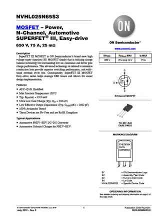
NVHL025N65S3 MOSFET Power, N-Channel, Automotive SUPERFET) III, Easy-drive 650 V, 75 A, 25 mW www.onsemi.com Description BVDSS RDS(on) MAX ID MAX SuperFET III MOSFET is ON Semiconductor s brand-new high voltage super-junction (SJ) MOSFET family that is utilizing charge 650 V 25 m @ 10 V 75 A balance technology for outstanding low on-resistance and lower gate charge performan
fcmt125n65s3.pdf
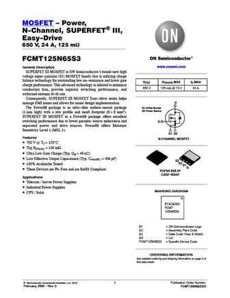
MOSFET Power, N-Channel, SUPERFET) III, Easy-Drive 650 V, 24 A, 125 mW FCMT125N65S3 www.onsemi.com General Description SUPERFET III MOSFET is ON Semiconductor s brand-new high voltage super-junction (SJ) MOSFET family that is utilizing charge balance technology for outstanding low on-resistance and lower gate VDSS RDS(ON) MAX ID MAX charge performance. This advanced technology
fcpf165n65s3l1.pdf
FCPF165N65S3L1 MOSFET Power, N-Channel, SUPERFET III, Easy Drive 650 V, 19 A, 165 mW Description www.onsemi.com SUPERFET III MOSFET is ON Semiconductor s brand-new high voltage super-junction (SJ) MOSFET family that is utilizing charge VDSS RDS(ON) MAX ID MAX balance technology for outstanding low on-resistance and lower gate 650 V 165 mW @ 10 V 19 A charge performance. This adv
fcpf125n65s3.pdf
CPF125N65S3 MOSFET Power, N-Channel, SUPERFET III, Easy Drive 650 V, 24 A, 125 mW Description www.onsemi.com SUPERFET III MOSFET is ON Semiconductor s brand-new high voltage super-junction (SJ) MOSFET family that is utilizing charge VDSS RDS(ON) MAX ID MAX balance technology for outstanding low on-resistance and lower gate 650 V 125 mW @ 10 V 24 A charge performance. This advanc
ntp095n65s3hf.pdf
NTP095N65S3HF MOSFET Power, N Channel, SUPERFET III, FRFET www.onsemi.com 650 V, 36 A, 95 mW Description VDSS RDS(ON) MAX ID MAX SUPERFET III MOSFET is ON Semiconductor s brand-new high voltage super-junction (SJ) MOSFET family that is utilizing charge 650 V 95 mW @ 10 V 36 A balance technology for outstanding low on-resistance and lower gate charge performance. This advance
5n65kl-ta3-t 5n65kg-ta3-t 5n65kl-tf3-t 5n65kg-tf3-t 5n65kl-tf1-t 5n65kg-tf1-t 5n65kl-tf2-t 5n65kg-tf2-t 5n65kl-tf3-t 5n65kg-tf3-t 5n65kl-tnd-r.pdf

UNISONIC TECHNOLOGIES CO., LTD 5N65K-MT Power MOSFET 5A, 650V N-CHANNEL POWER MOSFET DESCRIPTION The UTC 5N65K-MT is a high voltage power MOSFET designed to have better characteristics, such as fast switching time, low gate charge, low on-state resistance and high rugged avalanche characteristics. This power MOSFET is usually used in high speed switching applications at po
5n65k.pdf
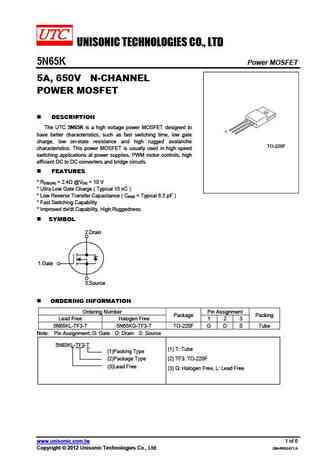
UNISONIC TECHNOLOGIES CO., LTD 5N65K Power MOSFET 5A, 650V N-CHANNEL POWER MOSFET DESCRIPTION The UTC 5N65K is a high voltage power MOSFET designed to 1 have better characteristics, such as fast switching time, low gate charge, low on-state resistance and high rugged avalanche TO-220F characteristics. This power MOSFET is usually used in high speed switching applications a
5n65l-ta3-t 5n65g-ta3-t 5n65l-tf3-t 5n65g-tf3-t 5n65l-tf1-t 5n65g-tf1-t 5n65l-tf2-t.pdf

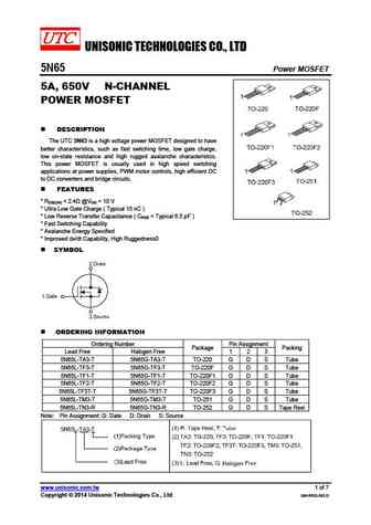
UNISONIC TECHNOLOGIES CO., LTD 5N65 Power MOSFET 5A, 650V N-CHANNEL POWER MOSFET DESCRIPTION The UTC 5N65 is a high voltage power MOSFET designed to have better characteristics, such as fast switching time, low gate charge, low on-state resistance and high rugged avalanche characteristics. This power MOSFET is usually used in high speed switching applications at power suppli
5n65l-tm3-t 5n65g-tm3-t 5n65l-tn3-r 5n65g-tn3-r 5n65g-tf2-t 5n65l-tf3t-t 5n65g-tf3t-t.pdf
UNISONIC TECHNOLOGIES CO., LTD 5N65 Power MOSFET 5A, 650V N-CHANNEL POWER MOSFET DESCRIPTION The UTC 5N65 is a high voltage power MOSFET designed to have better characteristics, such as fast switching time, low gate charge, low on-state resistance and high rugged avalanche characteristics. This power MOSFET is usually used in high speed switching applications at power suppli
5n65kl-tm3-t 5n65kg-tm3-t 5n65kl-tms-t 5n65kg-tms-t 5n65kl-tms2-t 5n65kg-tms2-t 5n65kl-tms4-t 5n65kg-tms4-t 5n65kl-tn3-r 5n65kg-tn3-r 5n65kg-tnd-r.pdf

UNISONIC TECHNOLOGIES CO., LTD 5N65K-MT Power MOSFET 5A, 650V N-CHANNEL POWER MOSFET DESCRIPTION The UTC 5N65K-MT is a high voltage power MOSFET designed to have better characteristics, such as fast switching time, low gate charge, low on-state resistance and high rugged avalanche characteristics. This power MOSFET is usually used in high speed switching applications at po
15n65.pdf
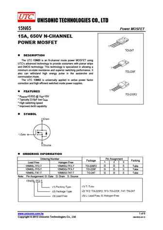
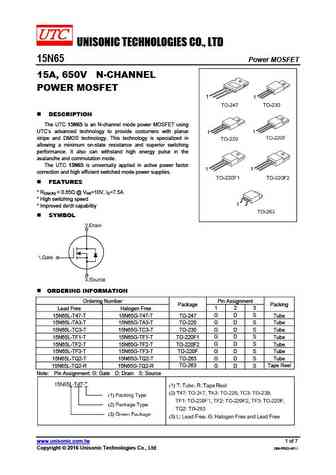
UNISONIC TECHNOLOGIES CO., LTD 15N65 Power MOSFET 15A, 650V N-CHANNEL POWER MOSFET DESCRIPTION The UTC 15N65 is an N-channel mode power MOSFET using UTC s advanced technology to provide costumers with planar stripe and DMOS technology. This technology is specialized in allowing a minimum on-state resistance and superior switching performance. It also can withstand high
15n65l-t47-t 15n65g-t47-t 15n65l-ta3-t 15n65g-ta3-t 15n65l-tc3-t 15n65g-tc3-t 15n65l-tf1-t 15n65g-tf1-t.pdf
UNISONIC TECHNOLOGIES CO., LTD 15N65 Power MOSFET 15A, 650V N-CHANNEL POWER MOSFET DESCRIPTION The UTC 15N65 is an N-channel mode power MOSFET using UTC s advanced technology to provide costumers with planar stripe and DMOS technology. This technology is specialized in allowing a minimum on-state resistance and superior switching performance. It also can withstand high en
15n65l-tf2-t 15n65g-tf2-t 15n65l-tf3-t 15n65g-tf3-t 15n65l-tq2-t 15n65g-tq2-t 15n65l-tq2-r 15n65g-tq2-r.pdf

UNISONIC TECHNOLOGIES CO., LTD 15N65 Power MOSFET 15A, 650V N-CHANNEL POWER MOSFET DESCRIPTION The UTC 15N65 is an N-channel mode power MOSFET using UTC s advanced technology to provide costumers with planar stripe and DMOS technology. This technology is specialized in allowing a minimum on-state resistance and superior switching performance. It also can withstand high en
5n65kl-tm3-t 5n65kg-tm3-t 5n65kl-tms-t 5n65kg-tms-t 5n65kl-tms2-t 5n65kg-tms2-t 5n65kl-tms4-t 5n65kg-tms4-t 5n65kl-tn3-r 5n65kg-tn3-r 5n65kl-tnd-r.pdf
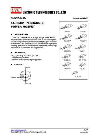
UNISONIC TECHNOLOGIES CO., LTD 5N65K-MTQ Power MOSFET 5A, 650V N-CHANNEL POWER MOSFET DESCRIPTION The UTC 5N65K-MTQ is a high voltage power MOSFET designed to have better characteristics, such as fast switching time, low gate charge, low on-state resistance and high rugged avalanche characteristics. This power MOSFET is usually used in high speed switching applications at
5n65kl-ta3-t 5n65kg-ta3-t 5n65kl-tf3-t 5n65kg-tf3-t 5n65kl-tf1-t 5n65kg-tf1-t 5n65kl-tf2-t 5n65kg-tf2-t 5n65kl-tf3-t 5n65kg-tf3-t 5n65kg-tnd-r.pdf

UNISONIC TECHNOLOGIES CO., LTD 5N65K-MTQ Power MOSFET 5A, 650V N-CHANNEL POWER MOSFET DESCRIPTION The UTC 5N65K-MTQ is a high voltage power MOSFET designed to have better characteristics, such as fast switching time, low gate charge, low on-state resistance and high rugged avalanche characteristics. This power MOSFET is usually used in high speed switching applications at
cjpf05n65.pdf
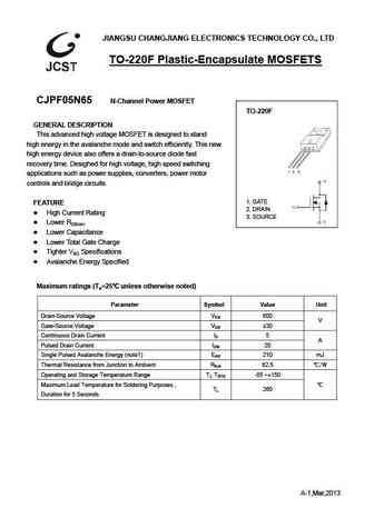
JIANGSU CHANGJIANG ELECTRONICS TECHNOLOGY CO., LTD TO-220F Plastic-Encapsulate MOSFETS CJPF05N65 N-Channel Power MOSFET TO-220F GENERAL DESCRIPTION This advanced high voltage MOSFET is designed to stand high energy in the avalanche mode and switch efficiently. This new high energy device also offers a drain-to-source diode fast recovery time. Desighed for high voltage, high s
kf5n65p-f.pdf
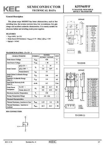
KF5N65P/F SEMICONDUCTOR N CHANNEL MOS FIELD TECHNICAL DATA EFFECT TRANSISTOR General Description KF5N65P A This planar stripe MOSFET has better characteristics, such as fast O C switching time, fast reverse recovery time, low on resistance, low gate F DIM MILLIMETERS charge and excellent avalanche characteristics. It is mainly suitable for E _ G A 9.9 + 0.2 electronic ballast
kf5n65d-i.pdf

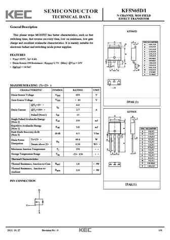
KF5N65D/I SEMICONDUCTOR N CHANNEL MOS FIELD TECHNICAL DATA EFFECT TRANSISTOR General Description KF5N65D This planar stripe MOSFET has better characteristics, such as fast switching time, fast reverse recovery time, low on resistance, low gate A K DIM MILLIMETERS charge and excellent avalanche characteristics. It is mainly suitable for L C D _ A 6.60 + 0.20 _ B 6.10 + 0.20 el
kf5n65i.pdf
KF5N65D/I SEMICONDUCTOR N CHANNEL MOS FIELD TECHNICAL DATA EFFECT TRANSISTOR General Description KF5N65D This planar stripe MOSFET has better characteristics, such as fast switching time, fast reverse recovery time, low on resistance, low gate A K DIM MILLIMETERS charge and excellent avalanche characteristics. It is mainly suitable for L C D _ A 6.60 + 0.20 _ B 6.10 + 0.20 el
kgf75n65kdf.pdf
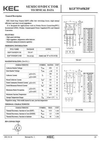
SEMICONDUCTOR KGF75N65KDF TECHNICAL DATA General Description B KEC Field Stop Trench IGBTs offer low switching losses, high energy A O S K efficiency and short circuit ruggedness. It is designed for applications such as Power Factor Correction(PFC), Inverterized MWO, Welder, Uninterrupted Power Supplies(UPS) and General DIM MILLIMETERS _ + A 15.90 0.30 Converters. _ B 5.00 + 0
cep05n65 ceb05n65 cef05n65.pdf
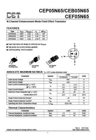
CEP05N65/CEB05N65 CEF05N65 N-Channel Enhancement Mode Field Effect Transistor FEATURES Type VDSS RDS(ON) ID @VGS CEP05N65 650V 2.4 4.5A 10V CEB05N65 650V 2.4 4.5A 10V CEF05N65 650V 2.4 4.5A d 10V D Super high dense cell design for extremely low RDS(ON). High power and current handing capability. Lead-free plating ; RoHS compliant. G S CEB SERIES CEP SERIES CEF SERIES TO
ceu05n65 ced05n65.pdf
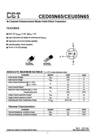
CED05N65/CEU05N65 N-Channel Enhancement Mode Field Effect Transistor FEATURES 650V, 4A, RDS(ON) = 2.4 @VGS = 10V. Super high dense cell design for extremely low RDS(ON). High power and current handing capability. D Lead-free plating ; RoHS compliant. TO-251 & TO-252 package. D G G S CEU SERIES CED SERIES S TO-252(D-PAK) TO-251(I-PAK) ABSOLUTE MAXIMUM RATINGS Tc = 25 C unless
sif5n65c.pdf
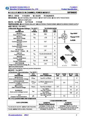
Shenzhen SI Semiconductors Co., LTD. Product Specification Shenzhen SI Semiconductors Co., LTD. Product Specification Shenzhen SI Semiconductors Co., LTD. Product Specification Shenzhen SI Semiconductors Co., LTD. Product Specification N- MOS / N-CHANNEL POWER MOSFET SIF5N65C N- MOS / N-CHANNEL POWER MOSFET SIF5N65C N- MOS / N-CHANN
jcs15n65fei jcs15n65bei jcs15n65sei jcs15n65cei.pdf
N R N-CHANNEL MOSFET JCS15N65EI Package MAIN CHARACTERISTICS ID 15A VDSS 650V Rdson-max 0.52 Vgs=10V Qg-Typ 52.3nC APPLICATIONS High efficiency switch mode power supplies Electronic lamp ballasts LED based on half bridge
jcs15n65fh.pdf
N R N-CHANNEL MOSFET JCS15N65H MAIN CHARACTERISTICS Package ID 15.0 A VDSS 650 V Rdson-Max 0.55 @Vgs=10V Qg-Typ 35.2 nC APPLICATIONS High efficiency switch mode power supplies Electronic lamp ballasts LED based on half bridge
mtn5n65fp.pdf
Spec. No. C716FP Issued Date 2010.03.12 CYStech Electronics Corp. Revised Date 2011.03.30 Page No. 1/ 10 N-Channel Enhancement Mode Power MOSFET BVDSS 650V RDS(ON) 2 (typ.) MTN5N65FP ID 5A Description The MTN5N65FP is a N-channel enhancement-mode MOSFET, providing the designer with the best combination of fast switching, ruggedized device design, low on-re
brf15n65.pdf
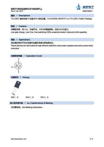
BRF15N65(BRCS15N65FL) Rev.C Feb.-2015 DATA SHEET / Descriptions TO-220FL N MOS N-CHANNEL MOSFET in a TO-220FL Plastic Package. / Features Crss 100 dv/dt Low gate charge, Low Crss ,Fast switching,100% avalanche tested, Improved dv/dt capability. / Appl
brf5n65.pdf
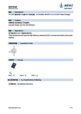
BRF5N65 Rev.D Nov.-2015 DATA SHEET / Descriptions TO-220F N MOS N-CHANNEL MOSFET in a TO-220F Plastic Package. / Features , , Low gate charge, low crss, fast switching. / Applications DC/DC These devices are well suited for high efficien
bri5n65.pdf
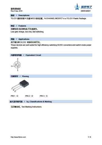
BRI5N65 Rev.A Sep.-2016 DATA SHEET / Descriptions TO-251 N MOS N-CHANNEL MOSFET in a TO-251 Plastic Package. / Features , , Low gate charge, low crss, fast switching. / Applications DC/DC These devices are well suited for high efficiency
brd5n65.pdf
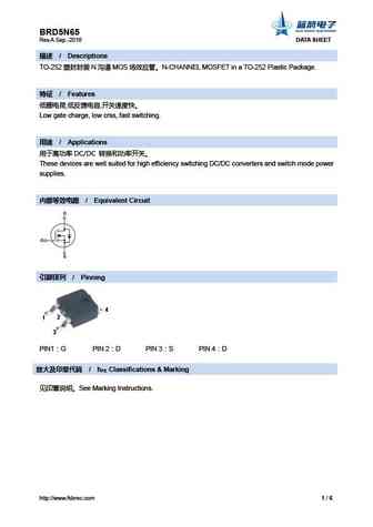
BRD5N65 Rev.A Sep.-2016 DATA SHEET / Descriptions TO-252 N MOS N-CHANNEL MOSFET in a TO-252 Plastic Package. / Features , , Low gate charge, low crss, fast switching. / Applications DC/DC These devices are well suited for high efficiency
5n65a 5n65af 5n65f 5n65g.pdf
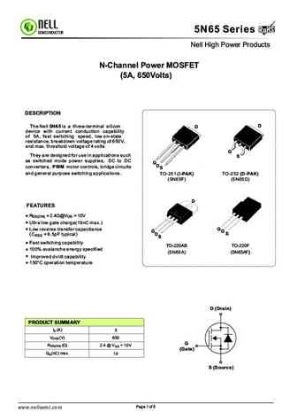
RoHS 5N65 Series RoHS SEMICONDUCTOR Nell High Power Products N-Channel Power MOSFET (5A, 650Volts) DESCRIPTION D The Nell 5N65 is a three-terminal silicon D device with current conduction capability of 5A, fast switching speed, low on-state resistance, breakdown voltage rating of 650V, and max. threshold voltage of 4 volts. G They are designed for use in applications such
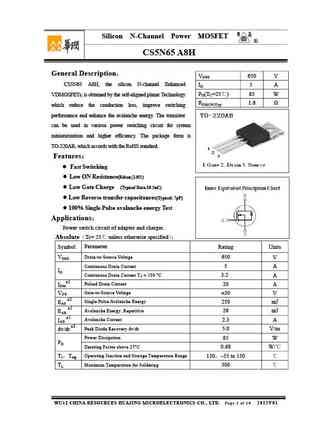
cs5n65 a8h.pdf

Silicon N-Channel Power MOSFET R CS5N65 A8H General Description VDSS 650 V CS5N65 A8H, the silicon N-channel Enhanced ID 5 A PD(TC=25 ) 85 W VDMOSFETs, is obtained by the self-aligned planar Technology RDS(ON)Typ 1.6 which reduce the conduction loss, improve switching performance and enhance the avalanche energy. The transistor can be used in various power s
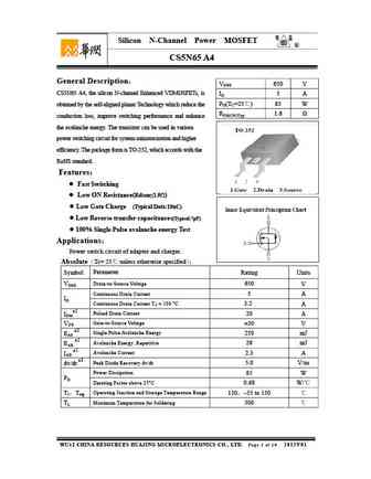
cs5n65 a4.pdf

Silicon N-Channel Power MOSFET R CS5N65 A4 General Description VDSS 650 V CS5N65 A4, the silicon N-channel Enhanced VDMOSFETs, is ID 5 A PD(TC=25 ) 85 W obtained by the self-aligned planar Technology which reduce the RDS(ON)Typ 1.6 conduction loss, improve switching performance and enhance the avalanche energy. The transistor can be used in various power sw
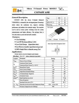
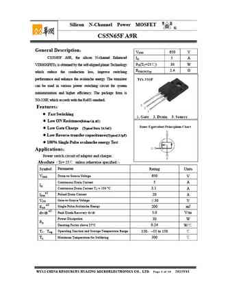
cs5n65f a9h.pdf
Silicon N-Channel Power MOSFET R CS5N65F A9H General Description VDSS 650 V CS5N65F A9H, the silicon N-channel Enhanced VDMOSFETs, ID 5 A PD(TC=25 ) 32 W is obtained by the self-aligned planar Technology which reduce RDS(ON)Typ 1.6 the conduction loss, improve switching performance and enhance the avalanche energy. The transistor can be used in various powe
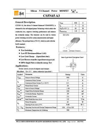
cs5n65 a3.pdf

Silicon N-Channel Power MOSFET R CS5N65 A3 General Description VDSS 650 V CS5N65 A3, the silicon N-channel Enhanced VDMOSFETs, is ID 5 A PD(TC=25 ) 85 W obtained by the self-aligned planar Technology which reduce the RDS(ON)Typ 1.6 conduction loss, improve switching performance and enhance the avalanche energy. The transistor can be used in various power swit
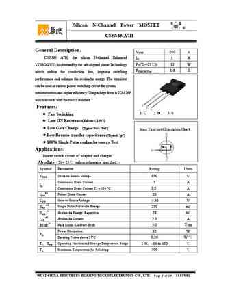
cs5n65 a7h.pdf

Silicon N-Channel Power MOSFET R CS5N65 A7H General Description VDSS 650 V CS5N65 A7H, the silicon N-channel Enhanced ID 5 A PD(TC=25 ) 32 W VDMOSFETs, is obtained by the self-aligned planar Technology RDS(ON)Typ 1.6 which reduce the conduction loss, improve switching performance and enhance the avalanche energy. The transistor can be used in various power
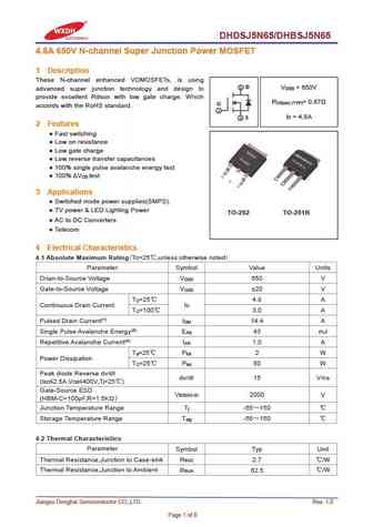
dhsj25n65f.pdf
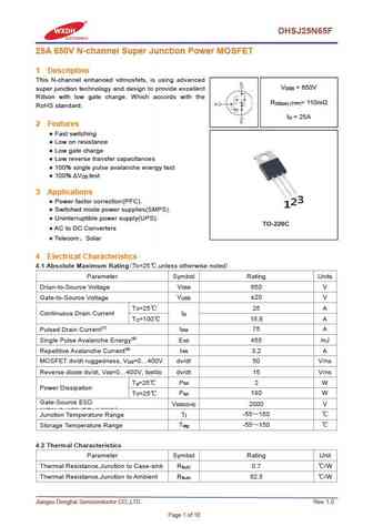
DHSJ25N65F 25A 650V N-channel Super Junction Power MOSFET 1 Description This N-channel enhanced vdmosfets, is using advanced V = 650V DSS super junction technology and design to provide excellent Rdson with low gate charge. Which accords with the R = 110m DS(on) (TYP) RoHS standard. I = 25A D 2 Features Fast switching Low on resistance Low gate charge Low reve
dhfsj5n65.pdf
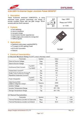
DHFSJ5N65 4.8A 650V N-channel Super Junction Power MOSFET 1 Description These N-channel enhanced VDMOSFETs, is using 2 D V = 650V DSS advanced super junction technology and design to provide excellent Rdson with low gate charge. Which R = 0.87 DS(on) (TYP) G accords with the RoHS standard. 1 I = 4.8A 3 S D 2 Features Fast switching Low on resistance Low gate cha
f5n65c.pdf
F5N65C 5A 650V N-channel Enhancement Mode Power MOSFET 1 Description These N-channel enhanced vdmosfets, is obtained by the self-aligned V DSS = 650V planar technology which reduce the conduction loss, improve switching I = 5A D performance and enhance the avalanche energy. Which accords with the RoHS standard.TO-220F provides insulation voltage rated at 2000V RMS R DS(on) TYP) =
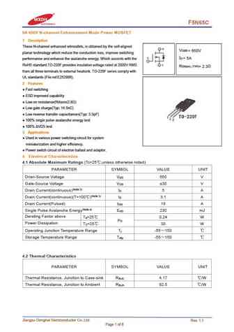
d5n65-xad.pdf
D5N65-XAD 5A 650V N-channel Enhancement Mode Power MOSFET 1 Description These N-channel enhanced vdmosfets, is obtained by the self-aligned V DSS = 650V planar technology which reduce the conduction loss, improve switching I = 5.0A D performance and enhance the avalanche energy. Which accords with the RoHS standard. TO-220F provides insulation voltage rated at 2000V R DS(on) TYP)
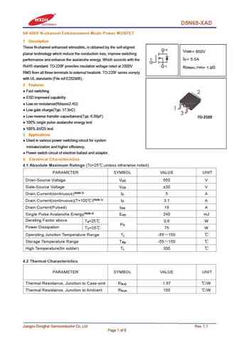
5n65c.pdf
5N65C 5A 650V N-channel Enhancement Mode Power MOSFET 1 Description These N-channel enhanced vdmosfets, is obtained by the self-aligned V DSS = 650V planar technology which reduce the conduction loss, improve switching I = 5A D performance and enhance the avalanche energy. Which accords with the RoHS standard. R DS(on) TYP) = 2.3 2 Features Fast switching ESD improve
b5n65.pdf
B5N65 5A 650V N-channel Enhancement Mode Power MOSFET 1 Description These N-channel enhanced vdmosfets, is obtained by the self-aligned V DSS = 650V planar technology which reduce the conduction loss, improve switching I = 5.0A D performance and enhance the avalanche energy. Which accords with the RoHS standard. R DS(on) TYP) = 1.9 2 Features Fast switching ESD impro
dhdsj5n65 dhbsj5n65.pdf
DHDSJ5N65/DHBSJ5N65 4.8A 650V N-channel Super Junction Power MOSFET 1 Description These N-channel enhanced VDMOSFETs, is using 2 D V = 650V DSS advanced super junction technology and design to provide excellent Rdson with low gate charge. Which R = 0.87 DS(on) (TYP) G accords with the RoHS standard. 1 I = 4.8A 3 S D 2 Features Fast switching Low on resistance Lo
svf5n65d svf5n65f.pdf

SVF5N65D/F 5A 650V N 2 SVF5N65D/F N MOS F-CellTM VDMOS 1 3 1. 2. 3.
svf5n65dtr svf5n65f.pdf
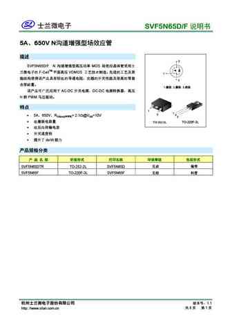
SVF5N65D/F 5A 650V N 2 SVF5N65D/F N MOS F-CellTM VDMOS 1 3 1. 2. 3.
wfd5n65l.pdf
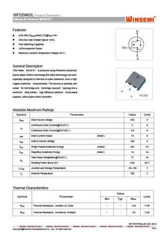
WFD5N65L Product Description Silicon N-Channel MOSFET Silicon N-Channel MOSFET Silicon N-Channel MOSFET Silicon N-Channel MOSFET Features D 5.0A,650V,R (Max2.7 )@V =10V DS(on) GS Ultra-low Gate charge(Typical 12nC) Fast Switching Capability G 100%Avalanche Tested Maximum Junction Temperature Range(150 ) S General Description This Power MOSFET is produced
wff5n65l.pdf
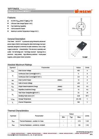
WFF5N65L Product Description Silicon N-Channel MOSFET Silicon N-Channel MOSFET Silicon N-Channel MOSFET Silicon N-Channel MOSFET Features D 5A,650V,R (Max2.7 )@V =10V DS(on) GS Ultra-low Gate charge(Typical 12nC) Fast Switching Capability G 100%Avalanche Tested Maximum Junction Temperature Range(150 ) S General Description This Power MOSFET is produced us
wfj5n65b.pdf
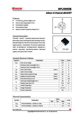
WFJ5N65B WFJ5N65B WFJ5N65B WFJ5N65B Silicon N-Channel MOSFET Silicon N-Channel MOSFET Silicon N-Channel MOSFET Silicon N-Channel MOSFET Features 4.5A,650V,R (Max2.5 )@V =10V DS(on) GS Ultra-low Gate charge(Typical13.3nC) Fast Switching Capability 100%Avalanche Tested Maximum Junction Temperature Range(150 ) General Description This Power MOSFET is produce
wff5n65b.pdf
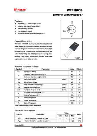
WFF5N65B WFF5N65B WFF5N65B WFF5N65B Silicon N-Channel MOSFET Silicon N-Channel MOSFET Silicon N-Channel MOSFET Silicon N-Channel MOSFET Features 4.5A,650V,R (Max2.5 )@V =10V DS(on) GS Ultra-low Gate charge(Typical13.3nC) Fast Switching Capability 100%Avalanche Tested Maximum Junction Temperature Range(150 ) General Description This Power MOSFET is produce
bl25n65-w bl25n65-f.pdf
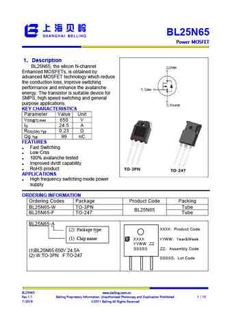
BL25N65 Power MOSFET Power MOSFET Power MOSFET Power MOSFET 1 Description BL25N65, the silicon N-channel Enhanced MOSFETs, is obtained by advanced MOSFET technology which reduce the conduction loss, improve switching performance and enhance the avalanche energy. The transistor is suitable device for SMPS, high speed switching and general purpose applica
chm05n65pagp.pdf
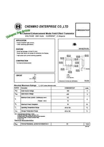
CHENMKO ENTERPRISE CO.,LTD CHM05N65PAGP N-Channel Enhancement Mode Field Effect Transistor VOLTAGE 650 Volts CURRENT 4 Ampere APPLICATION * Power MOSFET gate drivers. * Other switching applications. D-PAK(TO-252) FEATURE * Small flat package. D-PAK(TO-252) * Super high dense cell design for extremely low RDS(ON). .094 (2.40) .280 (7.10) * High power and current handing capabilit
fhp15n65a fhf15n65a.pdf
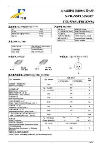
N N-CHANNEL MOSFET FHP15N65A /FHF15N65A MAIN CHARACTERISTICS FEATURES ID 15A Low gate charge VDSS 650V Crss ( 16pF) Low Crss (typical 16pF ) Rdson-typ @Vgs=10V 0.46 Fast switching Qg-typ 50nC 100% 100% avalanche tested dv/dt Improved dv

jfpc5n65c jffc5n65c.pdf
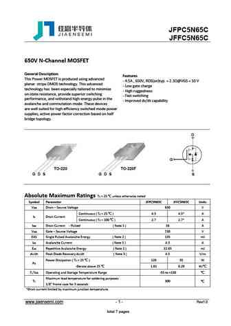
JFPC5N65C JFFC5N65C 650V N-Channel MOSFET General Description Features This Power MOSFET is produced using advanced - 4.5A , 650V, RDS(on)typ. = 2.3 @VGS = 10 V planar stripe DMOS technology. This advanced - Low gate charge technology has been especially tailored to minimize - High ruggedness on-state resistance, provide superior switching - Fast switching performance
slp5n65s slf5n65s.pdf
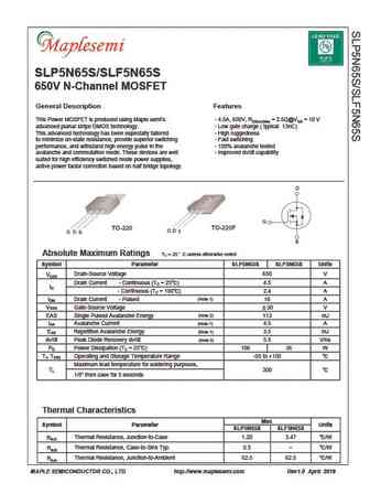
SLP5N65S/SLF5N65S 650V N-Channel MOSFET General Description Features This Power MOSFET is produced using Maple semi s - 4.5A, 650V, RDS(on)Max = 2.5 @VGS = 10 V advanced planar stripe DMOS technology. - Low gate charge ( typical 13nC) This advanced technology has been especially tailored - High ruggedness to minimize on-state resistance, provide superior switching - Fast switching per
slp5n65c slf5n65c.pdf
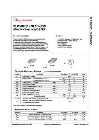
SLP5N65C / SLF5N65C 650V N-Channel MOSFET General Description Features This Power MOSFET is produced using Maple semi s - 4.5A, 650V, RDS(on)typ. = 2.6 @VGS = 10 V advanced planar stripe DMOS technology. - Low gate charge ( typical 16nC) This advanced technology has been especially tailored - High ruggedness to minimize on-state resistance, provide superior switching - Fast switching
sld5n65s slu5n65s.pdf
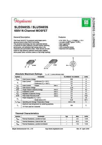
SLD5N65S / SLU5N65S SLD5N65S / SLU5N65S 650V N-Channel MOSFET General Description Features This Power MOSFET is produced using Maple semi s - 4.5A, 650V, RDS(on) = 2.5 @VGS = 10 V advanced planar stripe DMOS technology. - Low gate charge ( typical 13.3nC) This advanced technology has been especially tailored - High ruggedness to minimize on-state resistance, provide superior switching
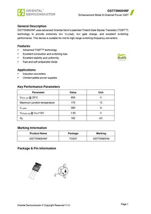
ost75n65hnf.pdf
OST75N65HNF Enhancement Mode N-Channel Power IGBT General Description OST75N65HNF uses advanced Oriental-Semi s patented Trident-Gate Bipolar Transistor (TGBTTM) technology to provide extremely low V (sat), low gate charge, and excellent switching CE performance. This device is suitable for mid to high range switching frequency converters. Features Advanced TGBTTM technolog
ost15n65krf.pdf

OST15N65KRF Enhancement Mode N-Channel Power IGBT General Description OST15N65KRF uses advanced Oriental-Semi s patented Trident-Gate Bipolar Transistor (TGBTTM) technology to provide extremely low V (sat), low gate charge, and excellent switching CE performance. This device is suitable for mid to high range switching frequency converters. Features Advanced TGBTTM technolog
ost75n65htnf.pdf
OST75N65HTNF Enhancement Mode N-Channel Power IGBT General Description OST75N65HTNF uses advanced Oriental-Semi s patented Trident-Gate Bipolar Transistor (TGBTTM) technology to provide extremely low V (sat), low gate charge, and excellent switching performance. CE This device is suitable for mid to high range switching frequency converters. Features Advanced TGBTTM technol
ost75n65hsxf.pdf

OST75N65HSXF Enhancement Mode N-Channel Power IGBT General Description OST75N65HSXF uses advanced Oriental-Semi s patented Trident-Gate Bipolar Transistor (TGBTTM) technology to provide extremely low V (sat), low gate charge, and excellent switching CE performance. This device is suitable for mid to high range switching frequency converters. Features Advanced TGBTTM technol
ost75n65hemf.pdf
OST75N65HEMF Enhancement Mode N-Channel Power IGBT General Description OST75N65HEMF uses advanced Oriental-Semi s patented Trident-Gate Bipolar Transistor (TGBTTM) technology to provide extremely low V (sat), low gate charge, and excellent switching CE performance. This device is suitable for mid to high range switching frequency converters. Features Advanced TGBTTM technol
ost15n65drf.pdf

OST15N65DRF Enhancement Mode N-Channel Power IGBT General Description OST15N65DRF uses advanced Oriental-Semi s patented Trident-Gate Bipolar Transistor (TGBTTM) technology to provide extremely low V (sat), low gate charge, and excellent switching CE performance. This device is suitable for mid to high range switching frequency converters. Features Advanced TGBTTM technolog
ost75n65hm2f.pdf

OST75N65HM2F Enhancement Mode N-Channel Power IGBT General Description OST75N65HM2F uses advanced Oriental-Semi s patented Trident-Gate Bipolar Transistor (TGBTTM) technology to provide extremely low V (sat), low gate charge, and excellent switching CE performance. This device is suitable for mid to high range switching frequency converters. Features Advanced TGBTTM technol
ost75n65hsvf.pdf
OST75N65HSVF Enhancement Mode N-Channel Power IGBT General Description OST75N65HSVF uses advanced Oriental-Semi s patented Trident-Gate Bipolar Transistor (TGBTTM) technology to provide extremely low V (sat), low gate charge, and excellent switching CE performance. This device is suitable for mid to high range switching frequency converters. Features Advanced TGBTTM technol
ost25n65pmf.pdf
OST25N65PMF Enhancement Mode N-Channel Power IGBT General Description OST25N65PMF uses advanced Oriental-Semi s patented Trident-Gate Bipolar Transistor (TGBTTM) technology to provide extremely low V (sat), low gate charge, and excellent switching CE performance. This device is suitable for mid to high range switching frequency converters. Features Advanced TGBTTM technolog
ost75n65hszf.pdf

OST75N65HSZF Enhancement Mode N-Channel Power IGBT General Description OST75N65HSZF uses advanced Oriental-Semi s patented Trident-Gate Bipolar Transistor (TGBTTM) technology to provide extremely low V (sat), low gate charge, and excellent switching CE performance. This device is suitable for mid to high range switching frequency converters. Features Advanced TGBTTM technol
ost75n65hem2f.pdf
OST75N65HEM2F Enhancement Mode N-Channel Power IGBT General Description OST75N65HEM2F uses advanced Oriental-Semi s patented Trident-Gate Bipolar Transistor (TGBTTM) technology to provide extremely low V (sat), low gate charge, and excellent switching CE performance. This device is suitable for mid to high range switching frequency converters. Features Advanced TGBTTM techn
ost15n65frf.pdf

OST15N65FRF Enhancement Mode N-Channel Power IGBT General Description OST15N65FRF uses advanced Oriental-Semi s patented Trident-Gate Bipolar Transistor (TGBTTM) technology to provide extremely low V (sat), low gate charge, and excellent switching CE performance. This device is suitable for mid to high range switching frequency converters. Features Advanced TGBTTM technolog
ost75n65hzf.pdf
OST75N65HZF Enhancement Mode N-Channel Power IGBT General Description OST75N65HZF uses advanced Oriental-Semi s patented Trident-Gate Bipolar Transistor (TGBTTM) technology to provide extremely low V (sat), low gate charge, and excellent switching CE performance. This device is suitable for mid to high range switching frequency converters. Features Advanced TGBTTM technolog
ost75n65hsnf.pdf

OST75N65HSNF Enhancement Mode N-Channel Power IGBT General Description OST75N65HSNF uses advanced Oriental-Semi s patented Trident-Gate Bipolar Transistor (TGBTTM) technology to provide extremely low V (sat), low gate charge, and excellent switching CE performance. This device is suitable for mid to high range switching frequency converters. Features Advanced TGBTTM technol
ost75n65hmf.pdf

OST75N65HMF Enhancement Mode N-Channel Power IGBT General Description OST75N65HMF uses advanced Oriental-Semi s patented Trident-Gate Bipolar Transistor (TGBTTM) technology to provide extremely low V (sat), low gate charge, and excellent switching CE performance. This device is suitable for mid to high range switching frequency converters. Features Advanced TGBTTM technolog
ost15n65prf.pdf
OST15N65PRF Enhancement Mode N-Channel Power IGBT General Description OST15N65PRF uses advanced Oriental-Semi s patented Trident-Gate Bipolar Transistor (TGBTTM) technology to provide extremely low V (sat), low gate charge, and excellent switching CE performance. This device is suitable for mid to high range switching frequency converters. Features Advanced TGBTTM technolog
ost75n65hsmf.pdf

OST75N65HSMF Enhancement Mode N-Channel Power IGBT General Description OST75N65HSMF uses advanced Oriental-Semi s patented Trident-Gate Bipolar Transistor (TGBTTM) technology to provide extremely low V (sat), low gate charge, and excellent switching CE performance. This device is suitable for mid to high range switching frequency converters. Features Advanced TGBTTM technol
ost75n65hlmf.pdf
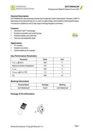
OST75N65HLMF Enhancement Mode N-Channel Power IGBT General Description OST75N65HLMF uses advanced Oriental-Semi s patented Trident-Gate Bipolar Transistor (TGBTTM) technology to provide extremely low V (sat), low gate charge, and excellent switching performance. CE This device is suitable for mid to high range switching frequency converters. Features Advanced TGBTTM technol
ost25n65fmf.pdf
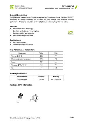
OST25N65FMF Enhancement Mode N-Channel Power IGBT General Description OST25N65FMF uses advanced Oriental-Semi s patented Trident-Gate Bipolar Transistor (TGBTTM) technology to provide extremely low V (sat), low gate charge, and excellent switching CE performance. This device is suitable for mid to high range switching frequency converters. Features Advanced TGBTTM technolog
pta05n65.pdf
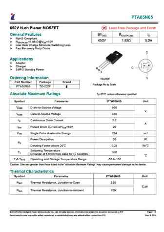
PTA05N65 650V N-ch Planar MOSFET General Features BVDSS RDS(ON),typ. ID RoHS Compliant 650V 1.85 5.0A RDS(ON),typ.=1.85 @VGS=10V Low Gate Charge Minimize Switching Loss Fast Recovery Body Diode Applications Adaptor Charger G SMPS Standby Power D S Ordering Information TO-220F Part Number Package Brand Package No to Scale PTA
swt45n65k2.pdf
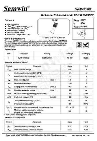
SW45N65K2 N-channel Enhanced mode TO-247 MOSFET TO-247 BVDSS 650V Features ID 45A High ruggedness RDS(ON) 61m Low RDS(ON) (Typ 61m )@VGS=10V Low Gate Charge (Typ 74nC) 2 Improved dv/dt Capability 1 100% Avalanche Tested 2 1 3 Application Charger, LED , UPS 1. Gate 2. Drain 3. Source 3 General Description This power MOSF
swf15n65d.pdf

SW15N65D N-channel Enhanced mode TO-220F MOSFET TO-220F BVDSS 650V Features ID 15A High ruggedness RDS(ON) 0.57 Low RDS(ON) (Typ 0.57 )@VGS=10V Low Gate Charge (Typ 57nC) 2 Improved dv/dt Capability 1 100% Avalanche Tested 2 1 3 Application LED , Charge, PC Power 1. Gate 2. Drain 3. Source 3 General Description This pow
swmn15n65j swd15n65j.pdf
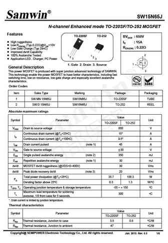
SW15N65J N-channel Enhanced mode TO-220SF/TO-252 MOSFET Features TO-220SF TO-252 BVDSS 650V High ruggedness ID 15A Low RDS(ON) (Typ 0.22 )@VGS=10V RDS(ON) 0.22 Low Gate Charge (Typ 29nC) Improved dv/dt Capability 2 100% Avalanche Tested 1 1 2 2 Application LED , Charger, PC Power 3 3 1 1. Gate 2. Drain 3. Source General Description This p
swt45n65k2f.pdf

SW45N65K2F N-channel Enhanced mode TO-247 MOSFET TO-247 BVDSS 650V Features ID 45A High ruggedness RDS(ON) 66m Low RDS(ON) (Typ 66m )@VGS=10V Low Gate Charge (Typ 74nC) 2 Improved dv/dt Capability 1 100% Avalanche Tested 2 1 3 Application Charger, LED , UPS 1. Gate 2. Drain 3. Source 3 General Description This power MOS
sw15n65d swf15n65d.pdf
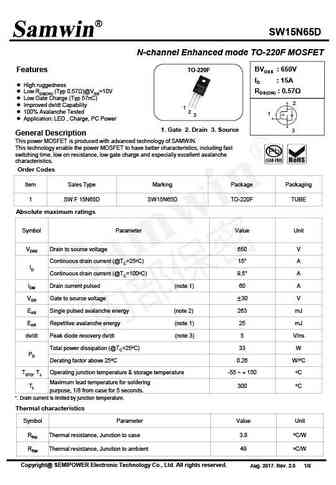
SW15N65D N-channel Enhanced mode TO-220F MOSFET TO-220F BVDSS 650V Features ID 15A High ruggedness RDS(ON) 0.57 Low RDS(ON) (Typ 0.57 )@VGS=10V Low Gate Charge (Typ 57nC) 2 Improved dv/dt Capability 1 100% Avalanche Tested 2 1 3 Application LED , Charge, PC Power 1. Gate 2. Drain 3. Source 3 General Description This pow
swd5n65k.pdf
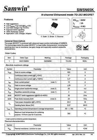
SW5N65K N-channel Enhanced mode TO-252 MOSFET Features TO-252 BVDSS 650V ID 5A High ruggedness Low RDS(ON) (Typ 0.8 )@VGS=10V RDS(ON) 0.8 Low Gate Charge (Typ 10.3nC) Improved dv/dt Capability 2 100% Avalanche Tested 1 2 Application LED, Charger, Adaptor 3 1. Gate 2. Drain 3. Source 1 3 General Description This power MOSF
hfs5n65sa.pdf
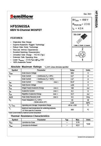
Dec. 2021 BVDSS = 650 V RDS(on) typ = 2.3 HFS5N65SA ID = 4.2 A 650V N-Channel MOSFET TO-220F FEATURES 1 Originative New Design 2 3 Superior Avalanche Rugged Technology 1.Gate 2. Drain 3. Source Robust Gate Oxide Technology Very Low Intrinsic Capacitances Excellent Switching Characteristics Unrivalled Gate Charge 14.2 nC (Typ.) Extended Safe Op
hfp5n65u.pdf
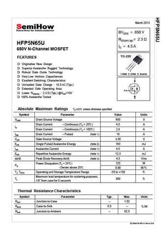
March 2013 BVDSS = 650 V RDS(on) typ HFP5N65U ID = 4.5 A 650V N-Channel MOSFET TO-220 FEATURES Originative New Design Superior Avalanche Rugged Technology 1 2 3 Robust Gate Oxide Technology 1.Gate 2. Drain 3. Source Very Low Intrinsic Capacitances Excellent Switching Characteristics Unrivalled Gate Charge 10.5 nC (Typ.) Extended Safe Operating Area
hfs5n65js.pdf
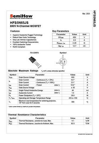
Mar. 2023 HFS5N65JS 650V N-Channel MOSFET Features Key Parameters Parameter Value Unit Superior Avalanche Rugged Technology BVDSS 650 V Robust Gate Oxide Technology Very Low Intrinsic Capacitances ID 4.0 A Excellent Switching Characteristics RDS(on), Typ 2.26 100% Avalanche Tested Qg, Typ 12.7 nC RoHS Compliant TO-220FS Symbol S D G Absolute Maximum
hfd5n65u.pdf
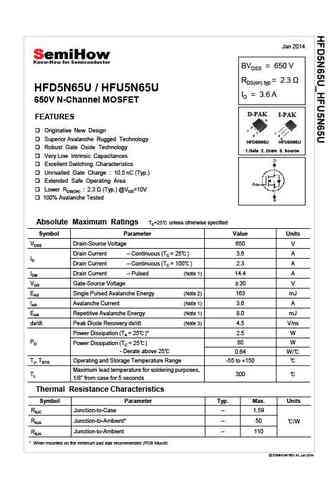
Jan 2014 BVDSS = 650 V RDS(on) typ = 2.3 HFD5N65U / HFU5N65U ID = 3.6 A 650V N-Channel MOSFET D-PAK I-PAK FEATURES 2 1 Originative New Design 1 3 2 3 Superior Avalanche Rugged Technology HFD5N65U HFU5N65U Robust Gate Oxide Technology 1.Gate 2. Drain 3. Source Very Low Intrinsic Capacitances Excellent Switching Characteristics Unrivalled Gate Charge 10.5 nC
hfs5n65u.pdf
March 2013 BVDSS = 650 V RDS(on) typ HFS5N65U ID = 4.5 A 650V N-Channel MOSFET TO-220F FEATURES Originative New Design Superior Avalanche Rugged Technology 1 2 3 Robust Gate Oxide Technology 1.Gate 2. Drain 3. Source Very Low Intrinsic Capacitances Excellent Switching Characteristics Unrivalled Gate Charge 10.5 nC (Typ.) Extended Safe Operating Area
hfw5n65u.pdf
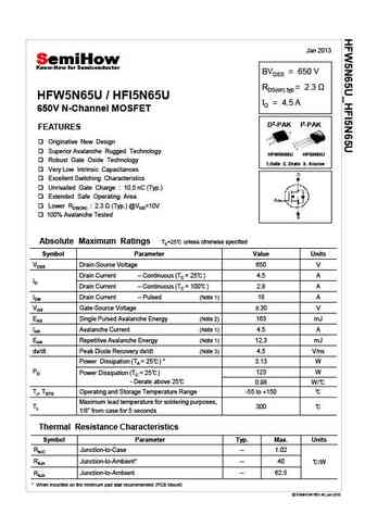
Jan 2013 BVDSS = 650 V RDS(on) typ HFW5N65U / HFI5N65U ID = 4.5 A 650V N-Channel MOSFET D2-PAK I2-PAK FEATURES Originative New Design Superior Avalanche Rugged Technology HFW5N65U HFI5N65U Robust Gate Oxide Technology 1.Gate 2. Drain 3. Source Very Low Intrinsic Capacitances Excellent Switching Characteristics Unrivalled Gate Charge 10.5 nC (Typ.) Exte
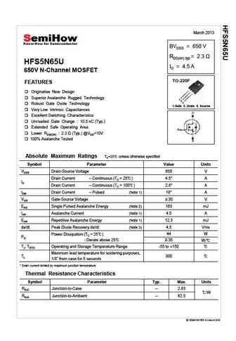
hfs5n65s.pdf
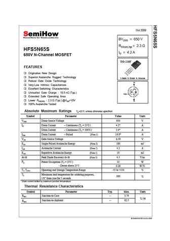
Oct 2009 BVDSS = 650 V RDS(on) typ = 2.3 HFS5N65S ID = 4.2 A 650V N-Channel MOSFET TO-220F FEATURES 1 Originative New Design 2 3 Superior Avalanche Rugged Technology 1.Gate 2. Drain 3. Source Robust Gate Oxide Technology Very Low Intrinsic Capacitances Excellent Switching Characteristics Unrivalled Gate Charge 10.5 nC (Typ.) Unrivalled Gate Charge 10 5 nC (Typ )
hfp5n65s.pdf
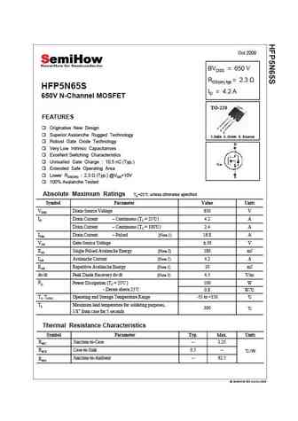
Oct 2009 BVDSS = 650 V RDS(on) typ = 2.3 HFP5N65S ID = 4.2 A 650V N-Channel MOSFET TO-220 FEATURES Originative New Design 1 2 3 Superior Avalanche Rugged Technology 1.Gate 2. Drain 3. Source Robust Gate Oxide Technology Very Low Intrinsic Capacitances Excellent Switching Characteristics Unrivalled Gate Charge 10.5 nC (Typ.) Unrivalled Gate Charge 10 5 nC (Typ )
hfu5n65sa hfd5n65sa.pdf
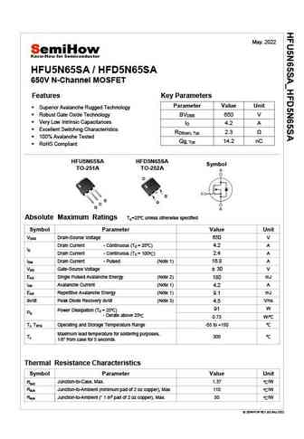
May. 2022 HFU5N65SA / HFD5N65SA 650V N-Channel MOSFET Features Key Parameters Parameter Value Unit Superior Avalanche Rugged Technology BVDSS 650 V Robust Gate Oxide Technology Very Low Intrinsic Capacitances ID 4.2 A Excellent Switching Characteristics RDS(on), Typ 2.3 100% Avalanche Tested Qg, Typ 14.2 nC RoHS Compliant HFU5N65SA HFD5N65SA Symbol TO
hia75n65h-sa.pdf
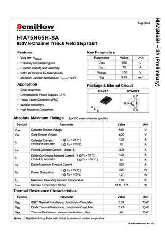
Aug 2023 HIA75N65H-SA 650V N-Channel Trench Field Stop IGBT Features Key Parameters Very Low VCE(sat) Parameter Value Unit VCES 650 V Extremely low switching loss IC 75 A Excellent stability and uniformity VCE(sat) 1.50 V Soft Fast Reverse Recovery Diode Etot 3.79 mJ Maximum Junction temperature, TJ(max)=175 Application Package & Internal Circuit Solar
hfw5n65s.pdf
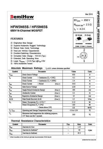
Mar 2010 BVDSS = 650 V RDS(on) typ HFW5N65S / HFI5N65S ID = 4.2 A 650V N-Channel MOSFET D2-PAK I2-PAK FEATURES Originative New Design HFW5N65S HFI5N65S Superior Avalanche Rugged Technology 1.Gate 2. Drain 3. Source Robust Gate Oxide Technology Very Low Intrinsic Capacitances Excellent Switching Characteristics Unrivalled Gate Charge 10.5 nC (Typ.) Extended Saf
hfd5n65s.pdf
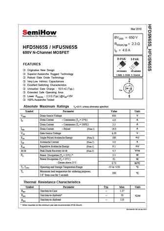
Mar 2010 BVDSS = 650 V RDS(on) typ = 2.3 HFD5N65S / HFU5N65S ID = 4.0 A 650V N-Channel MOSFET D-PAK I-PAK 2 2 FEATURES 1 1 3 2 3 Originative New Design HFD5N65S HFU5N65S Superior Avalanche Rugged Technology 1.Gate 2. Drain 3. Source Robust Gate Oxide Technology Very Low Intrinsic Capacitances Excellent Switching Characteristics Unrivalled Gate Charge 10.5 nC (Typ
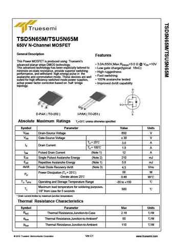
tsd5n65m tsu5n65m.pdf
TSD5N65M/TSU5N65M 650V N-Channel MOSFET General Description Features This Power MOSFET is produced using Truesemi s 3.0A,650V,Max.RDS(on)=3.0 @ VGS =10V advanced planar stripe DMOS technology. This advanced technology has been especially tailored to Low gate charge(typical 16nC) minimize on-state resistance, provide superior switching High ruggedness performance, and
tsp5n65m tsf5n65m.pdf
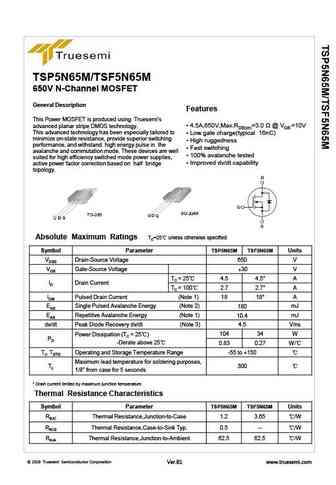
TSP5N65M/TSF5N65M 650V N-Channel MOSFET General Description Features This Power MOSFET is produced using Truesemi s 4.5A,650V,Max.RDS(on)=3.0 @ VGS =10V advanced planar stripe DMOS technology. This advanced technology has been especially tailored to Low gate charge(typical 16nC) minimize on-state resistance, provide superior switching High ruggedness perform
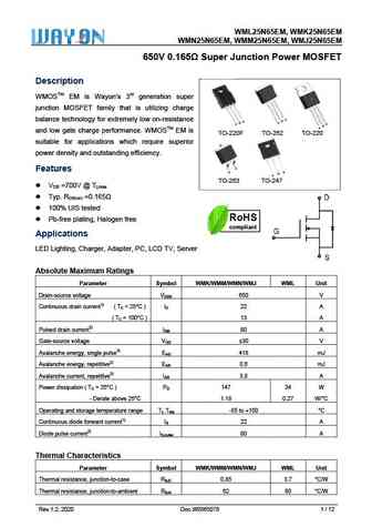
wml15n65c4 wmk15n65c4 wmm15n65c4 wmn15n65c4 wmp15n65c4 wmo15n65c4.pdf

WML1 MM15N65C 15N65C4, WMK15N65C4, WM C4 WMN15N65C4, WMP15N65C4, WM C4 MO15N65C 650V n Power MOSFET V 0.26 Super Junction Descrip ption WMOSTM C4 is Wa 4th generation super ayon s n junction MOSFET fa that is utilizing charge M amily S balance te or extremely esistance echnology fo y low on-re D S D G G G S D G and low ga charge performanc WMOSTM C4
wml25n65em wmk25n65em wmn25n65em wmm25n65em wmj25n65em.pdf
WML25N6 MK25N65EM W 65EM, WM WMN25 WMM25N6 MJ25N65EM 5N65EM, W 65EM, WM 650V 0.165 S 0 Super Junction Power MOSFET Descrip ption WMOSTM EM is Wayon s 3rd generation super W n junction MOSFET fa that is utilizing charge M amily S balance te or extremely esistance echnology fo y low on-re S D D G G G S D G T and low ga ce. WMOSTM EM is ate charge perf
wml15n65f2 wmk15n65f2 wmm15n65f2 wmn15n65f2 wmp15n65f2 wmo15n65f2.pdf
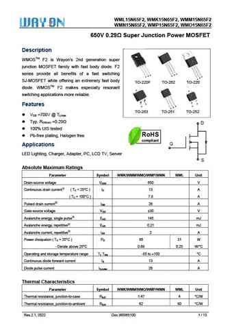
WML N65F2, WM F2 L15N65F2, WMK15N MM15N65F WMN , WMP15N MO15N65F N15N65F2, N65F2, WM F2 650V Super Ju MOSFET V 0.29 S unction Power M T Descrip ption WMOSTM F2 is Wa 2nd generation super ayon s junction MOSFET fam with fa body di F2 M mily ast iode. S series pro all benefits of a fast switching ovide b f s D S D G G G S D G SJ-MOSFE while of an extr
wml15n65c2 wmk15n65c2 wmm15n65c2 wmn15n65c2 wmp15n65c2 wmo15n65c2.pdf
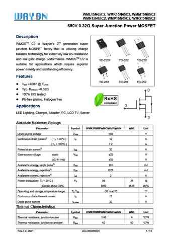
WML1 MM15N65C 15N65C2, WMK15N65C2, WM C2 WMN15N65C2, WMP15N65C2, WM C2 MO15N65C 650V n Power MOSFET V 0.32 Super Junction Descrip ption WMOSTM C2 is Wa 2nd generation super ayon s n junction MOSFET fa that is utilizing charge M amily S balance te or extremely esistance echnology fo y low on-re D S D G G G S D G and low ga charge performanc WMOSTM C2
cs5n65a8h.pdf
Silicon N-Channel Power MOSFET R CS5N65 A8H General Description VDSS 650 V CS5N65 A8H, the silicon N-channel Enhanced ID 5 A PD(TC=25 ) 85 W VDMOSFETs, is obtained by the self-aligned planar Technology RDS(ON)Typ 1.6 which reduce the conduction loss, improve switching performance and enhance the avalanche energy. The transistor can be used in various power s
cs5n65a7h.pdf
Silicon N-Channel Power MOSFET R CS5N65 A7H General Description VDSS 650 V CS5N65 A7H, the silicon N-channel Enhanced ID 5 A PD(TC=25 ) 32 W VDMOSFETs, is obtained by the self-aligned planar Technology RDS(ON)Typ 1.6 which reduce the conduction loss, improve switching performance and enhance the avalanche energy. The transistor can be used in various power
cs5n65a4.pdf
Silicon N-Channel Power MOSFET R CS5N65 A4 General Description VDSS 650 V CS5N65 A4, the silicon N-channel Enhanced VDMOSFETs, is ID 5 A PD(TC=25 ) 85 W obtained by the self-aligned planar Technology which reduce the RDS(ON)Typ 1.6 conduction loss, improve switching performance and enhance the avalanche energy. The transistor can be used in various power sw
cs5n65a3.pdf
Silicon N-Channel Power MOSFET R CS5N65 A3 General Description VDSS 650 V CS5N65 A3, the silicon N-channel Enhanced VDMOSFETs, is ID 5 A PD(TC=25 ) 85 W obtained by the self-aligned planar Technology which reduce the RDS(ON)Typ 1.6 conduction loss, improve switching performance and enhance the avalanche energy. The transistor can be used in various power swit
cs5n65fa9h.pdf
Silicon N-Channel Power MOSFET R CS5N65F A9H General Description VDSS 650 V CS5N65F A9H, the silicon N-channel Enhanced ID 5 A PD(TC=25 ) 32 W VDMOSFETs, is obtained by the self-aligned planar Technology RDS(ON)Typ 1.6 which reduce the conduction loss, improve switching performance and enhance the avalanche energy. The transistor can be used in various powe
cs5n65fa9r.pdf
Silicon N-Channel Power MOSFET R CS5N65F A9R General Description VDSS 650 V CS5N65F A9R, the silicon N-channel Enhanced ID 5 A PD(TC=25 ) 30 W VDMOSFETs, is obtained by the self-aligned planar Technology RDS(ON)Typ 2.4 which reduce the conduction loss, improve switching performance and enhance the avalanche energy. The transistor can be used in various power
dm5n65e.pdf
N MOS /N-Channel Power MOSFET DM5N65E RoHS FEATURES LOW ON-RESISTANCE FAST SWITCHING HIGH INPUT RESISTANCE RoHS COMPLIANT APPLICATION ELECTRONIC BALLAST ELECTRONIC TRANSFORMER SWITCH MODE POWER SUPPLY
cs5n65f cs5n65p cs5n65u cs5n65d.pdf
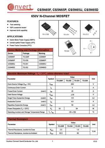
nvert Suzhou Convert Semiconductor Co ., Ltd. CS5N65F, CS5N65P, CS5N65U, CS5N65D 650V N-Channel MOSFET FEATURES Fast switching 100% avalanche tested Improved dv/dt capability APPLICATIONS Switch Mode Power Supply (SMPS) Uninterruptible Power Supply (UPS) Power Factor Correction (PFC) Device Marking and Package Information Device Package Marking CS5N65F TO-2
fir5n65fg.pdf
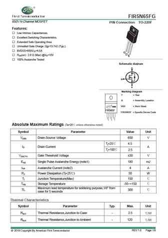
FIR5N65FG 650V N-Channel MOSFET PIN Connection TO-220F Features Low Intrinsic Capacitances. Excellent Switching Characteristics. Extended Safe Operating Area. Unrivalled Gate Charge Qg=13.7nC (Typ.). BVDSS=650V,ID=4.5A G D S RDS(on) 2.6 (Max) @VG=10V 100% Avalanche Tested g Schematic dia ram D G S Marking Diagram Y = Year A = Assem
smf5n65.pdf
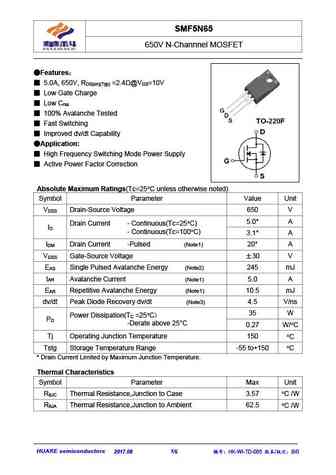
SMF5N65 650V N-Channnel MOSFET Features 5.0A, 650V, R =2.4 @V =10V DS(on)(Typ) GS Low Gate Charge Low C rss 100% Avalanche Tested Fast Switching Improved dv/dt Capability Application High Frequency Switching Mode Power Supply Active Power Factor Correction Absolute Maximum Ratings(Tc=25 C unless otherwise noted) Symbol Parameter Value
hf5n65.pdf
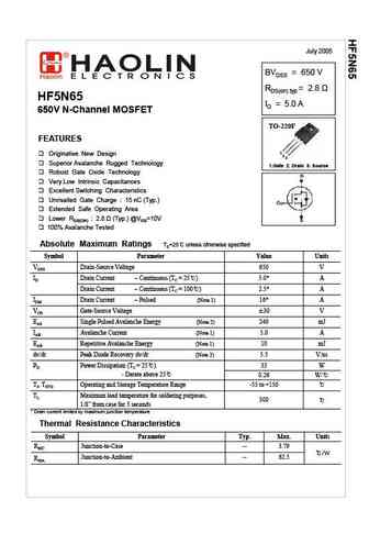
July 2005 BVDSS = 650 V RDS(on) typ = 2.8 HF5N65 ID = 5.0 A 650V N-Channel MOSFET TO-220F FEATURES 1 Originative New Design 2 3 Superior Avalanche Rugged Technology 1.Gate 2. Drain 3. Source Robust Gate Oxide Technology Very Low Intrinsic Capacitances Excellent Switching Characteristics Unrivalled Gate Charge 15 nC (Typ.) Extended Safe Operati
jjt15n65ss.pdf
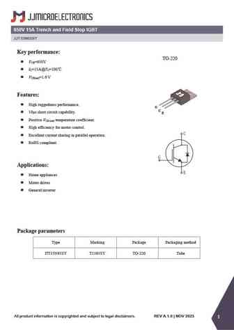
650V 15A Trench and Field Stop IGBT JJT15N65SS Key performance V =650V CE TO-220F I =15A@T =100 C C V =1.6 V CE(sat) Features High ruggedness performance. 10 s short circuit capability. G C E Positive V temperature coefficient. CE (sat) High efficiency for motor control. Excellent current sharing in parallel operation. RoHS compliant
jjt75n65hcn.pdf
650V 75A Trench and Field Stop IGBT JJT75N65HCN Key performance TO-263 V =650V CE I =75A@T =100 C C V =1.8V CE(sat) C Features Trench and field-stop technology. G Easy parallel switching capability. E Benefits High efficiency for inverters. High ruggedness performance. RoHS compliant. Applications Hair removal device Flash lig
jjt15n65sg.pdf
650V 15A Trench and Field Stop IGBT JJT15N65SG Key performance TO-220A V =650V CE I =15A@T =100 C C V =1.6 V CE(sat) Features High ruggedness performance. G C 10 s short circuit capability. E Positive V temperature coefficient. CE (sat) High efficiency for motor control. Excellent current sharing in parallel operation. RoHS compliant
jjt15n65sc.pdf
650V 15A Trench and Field Stop IGBT JJT15N65SC Key performance TO-263 V =650V CE I =15A@T =100 C C V =1.6 V CE(sat) C Features G High ruggedness performance. E 10 s short circuit capability. Positive V temperature coefficient. CE (sat) High efficiency for motor control. Excellent current sharing in parallel operation. RoHS compliant.
jjt15n65sy.pdf
650V 15A Trench and Field Stop IGBT JJT15N65SY Key performance TO-220 V =650V CE I =15A@T =100 C C V =1.6 V CE(sat) Features High ruggedness performance. G C 10 s short circuit capability. E Positive V temperature coefficient. CE (sat) High efficiency for motor control. Excellent current sharing in parallel operation. RoHS compliant.
jjt75n65he.pdf
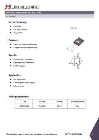
650V 75A Trench and Field Stop IGBT JJT75N65HE Key performance V =650V CE TO-247 I =75A@T =100 C C V =1.8V CE(sat) Features Trench and field-stop technology. Easy parallel switching capability. G C E Benefits High efficiency for inverters. High ruggedness performance. RoHS compliant. Applications PFC applications Uninterruptib
lnc5n65b lnd5n65b lng5n65b lnh5n65b.pdf
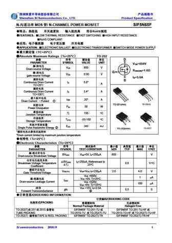
LNC5N65B LND5N65B LNG5N65B LNH5N65B Lonten N-channel 650V, 5A Power MOSFET Description Product Summary The Power MOSFET is fabricated using the V 650V DSS advanced planar VDMOS technology. The I 5A D resulting device has low conduction resistance, R 2.1 DS(on),max superior switching performance and high avalanche Q 14.5 nC g,typ energy. Features Low R DS(on) Low gate ch
ptf5n65.pdf
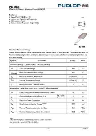
PTF5 N65 65 0V/5 A N-Channel A dv anced Power MOSFET Features RDS(on) (Typical 1.9 )@VGS=10V Improved dv/dt Capability, High Ruggedness 100% Avalanche Tested Maximum Junction Temperature Range (150 C) G D S TO-220F Absolute Maximum Ratings Stresses exceeding Maximum Ratings may damage the device. Maximum Ratings are stress ratings only. Functional operation above t
spf15n65t1t1tl.pdf

SPF15N65T1T1TL 650V /15A Trench Field Stop IGBT Features V 650 V CE Max Junction Temperature 150 C High breakdown voltage up to 650V for I 15 A C improved reliability V I =15A 1.65 V CE(SAT) C Short Circuit Rated Very Low Saturation Voltage V = 1.65V (Typ.) @ I = 15A CE(SAT) C Soft current turn-off waveforms Applications Soft switching applicat
spd15n65t1t0tl.pdf
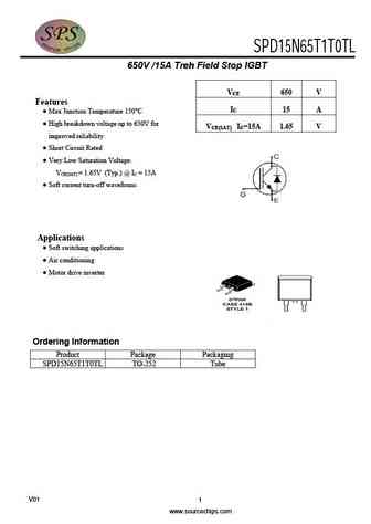
SPD15N65T1T0TL 650V /15A Tren ch Field Stop IGBT V 650 V CE Features I 15 A C Max Junction Temperature 150 C High breakdown voltage up to 650V for V I =15A 1.65 V CE(SAT) C improved reliability Short Circuit Rated Very Low Saturation Voltage V = 1.65V (Typ.) @ I = 15A CE(SAT) C Soft current turn-off waveforms Applications Soft switching appli
smirf5n65.pdf
SMIRF5N65 30V /36A Single N Power MOSFET N-Channel Enhancement Mode Power MOSFET Description ID 5A SMIRF5N65 is an N-channel enhancement mode power MOS field effect transistor. The improved VDSS 650V planar stripe cell and the improved guard ring terminal have been especially tailored to minimize Rdson max 2.3 (VGS=10V, ID=2.5A) on-state resistance, provide superior
spf15n65t1t2tl.pdf
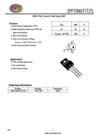
SPF15N65T1T2TL 650V /15A Trench Field Stop IGBT Features V 650 V CE Max Junction Temperature 150 C High breakdown voltage up to 650V for I 15 A C improved reliability V I =15A 1.65 V CE(SAT) C Short Circuit Rated Very Low Saturation Voltage V = 1.65V (Typ.) @ I = 15A CE(SAT) C Soft current turn-off waveforms Applications Soft switching applicat
dgw75n65ctl1.pdf
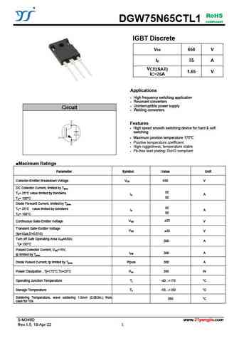
RoHS DGW75N65CTL1 COMPLIANT IGBT Discrete V 650 V CE I 75 A C V CE(SAT) 1.65 V I = A C 75 Applications High frequency switching application Resonant converters Uninterruptible power supply Circuit Welding converters Features High speed smooth switching device for hard & soft switching Maximum junction temperature 175 Pos
dgw15n65ctl.pdf
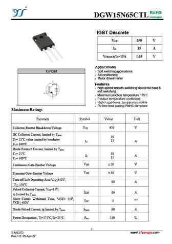
DGW15N65CTL RoHS COMPLIANT IGBT Descrete V 650 V CE I 15 A C V I = A 1.65 V CE(SAT) C 15 Applications Circuit Soft switchingapplications Airconditioning Motor driveinverter Features High speed smooth switching device for hard & soft switching Maximum junction temperature 175 Positive temperature coefficient High ruggedness, temp
dgp15n65ctl.pdf
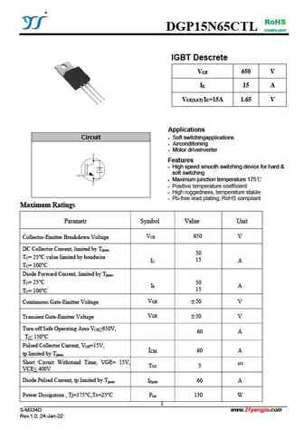
RoHS DGP15N65CTL COMPLIANT IGBT Descrete V 650 V CE I 15 A C V I = A 1.65 V CE(SAT) C 15 Applications Circuit Soft switchingapplications Airconditioning Motor driveinverter Features High speed smooth switching device for hard & soft switching Maximum junction temperature 175 Positive temperature coefficient High ruggedness, te
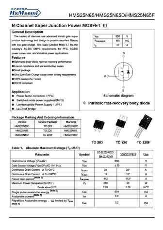
hms25n65 hms25n65d hms25n65f.pdf
HMS25N65/HMS25N65D/HMS25N65F N-Channel Super Junction Power MOSFET General Description The series of devices use advanced trench gate super V 650 V DS junction technology and design to provide excellent RDS(ON) R 115 m DS(ON)TYP with low gate charge. This super junction MOSFET fits the ID 2 A industry s AC-DC SMPS requirements for PFC, AC/DC power conversion, and ind
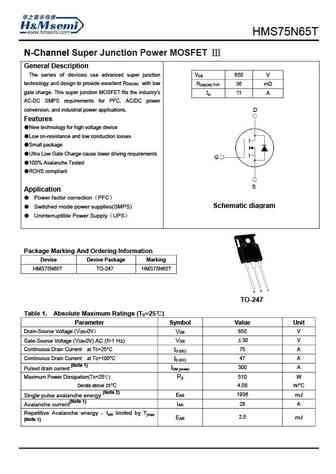
hms75n65t.pdf
HMS75N65T N-Channel Super Junction Power MOSFET General Description The series of devices use advanced super junction V 650 V DS technology and design to provide excellent RDS(ON) with low R 36 m DS(ON) TYP. gate charge. This super junction MOSFET fits the industry s ID 75 A AC-DC SMPS requirements for PFC, AC/DC power conversion, and industrial power applications.
hms15n65a.pdf
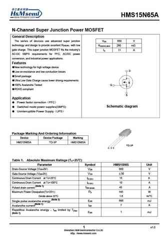
HMS15N65A N-Channel Super Junction Power MOSFET General Description The series of devices use advanced super junction VDS 650 V technology and design to provide excellent RDS(ON) with low RDS(ON) MAX 260 m gate charge. This super junction MOSFET fits the industry s ID 1 A AC-DC SMPS requirements for PFC, AC/DC power conversion, and industrial power applications. Features
hms15n65i hms15n65k.pdf
HMS15N65I / HMS15N65K N-Channel Super Junction Power MOSFET General Description The series of devices use advanced trench gate super V 650 V DS junction technology and design to provide excellent RDS(ON) R 220 m DS(ON)TYP with low gate charge. This super junction MOSFET fits the ID 15 A industry s AC-DC SMPS requirements for PFC, AC/DC power conversion, and industrial
hm5n65 hm5n65f.pdf
/ / 650V N-Channel MOSFET General Description Features This Power MOSFET is produced using SL semi s 4.5A, 650V, RDS(on) = 3.0 @VGS = 10 V advanced planar stripe DMOS technology. Low gate charge ( typical 15nC) This advanced technology has been espe cially tailored to High ruggedness minimize o n-state r esistance, pr ovide superior switchi
hm5n65k hm5n65i.pdf
HM5N65K/HM5N65I HM5N65K / HM5N65I 650V N-Channel MOSFET General Description Features This Power MOSFET is produced using SL semi s 4.5A, 650V, RDS(on) = 3.0 @VGS = 10 V advanced planar stripe DMOS technology. Low gate charge ( typical 15nC) This advanced technology has been espe cially tailored to High ruggedness minimize o n-state r esistance, pr ovide superior switchi
hms15n65 hms15n65f hms15n65d.pdf
HMS15N65D, HMS15N65, HMS15N65F N-Channel Super Junction Power MOSFET General Description The series of devices use advanced super junction VDS 650 V technology and design to provide excellent RDS(ON) with low RDS(ON) MAX 260 m gate charge. This super junction MOSFET fits the industry s ID 15 A AC-DC SMPS requirements for PFC, AC/DC power conversion, and industrial power ap
mpf5n65 mp5n65 mdp5n65 mdt5n65.pdf
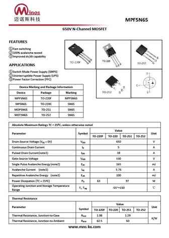
650V N-Channel MOSFET FEATURES Fast switching 100% avalanche tested Improved dv/dt capability APPLICATIONS Switch Mode Power Supply (SMPS) Uninterruptible Power Supply (UPS) Power Factor Correction (PFC) Device Marking and Package Information Device Package Marking MPF5N65 TO-220F MPF5N65 MP5N65 TO-220C 5N65 MDP5N65 TO-251 5N65 MDT5N65 TO-252 5N65 Absolute Maxim
fxn5n65d.pdf
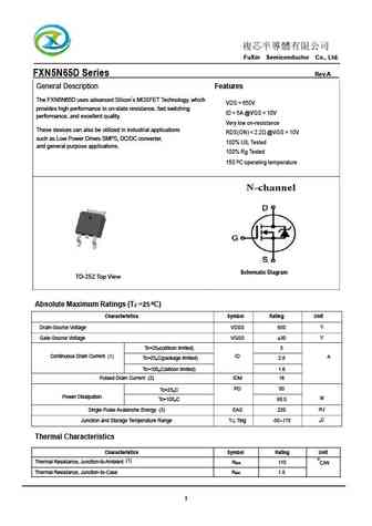
FuXin Semiconductor Co., Ltd. FXN5N65D Series Rev.A General Description Features The FXN5N65D uses advanced Silicon s MOSFET Technology, which VDS = 650V provides high performance in on-state resistance, fast switching ID = 5A @VGS = 10V performance, and excellent quality. Very low on-resistance These devices can also be utilized in industria
fxn5n65f.pdf
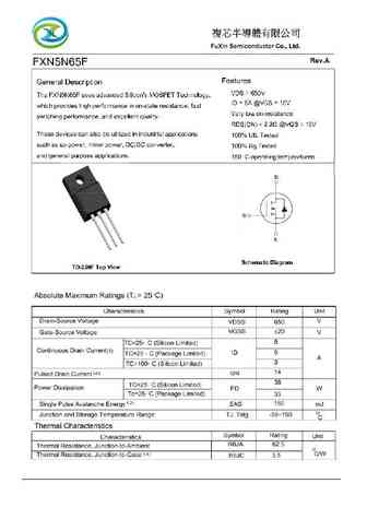
FXN5N65F Electrical Characteristics (TJ =25oC) Characteristics Symbol Test Condition Min Typ Max Unit Static Characteristics Drain-Source Breakdown Voltage BVDSS ID = 250 A, VGS = 0V 660 - - V Gate Threshold Voltage VGS(th) - 2.0 4.0 VDS = VGS, ID = 250 A Drain Cut-Off Current IDSS VDS = 650V, VGS = 0V 1.0 - - A VGS = 30V, VDS = 0V - 0.1 Gate Leakage Current
fxn5n65fm.pdf
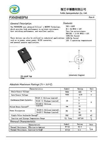
FuXin Semiconductor Co., Ltd. Rev.A FXN5N65FM Features General Description VDS = 650V The FXN5N65FM uses advanced Silicon s MOSFET Technology, which provides high performance in on-state resistance, ID = 5A @VGS = 10V fast switching performance, and excellent quality. Very low on-resistance RDS(ON)
mpbp15n65ef mpba15n65ef mpbc15n65ef.pdf
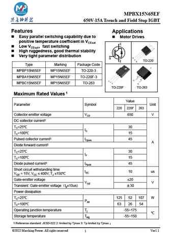
MPBX15N65EF 650V-15A Trench and Field Stop IGBT Features Applications Easy parallel switching capability due to Motor Drives positive temperature coefficient in VCEsat Low VCEsat fast switching High ruggedness, good thermal stability Very tight parameter distribution G C TO-220 E Type Marking Package Code C MPBP15N65EF MP15N65EF TO-220-3 MPBA15N65EF MP15N
mpbw75n65e.pdf
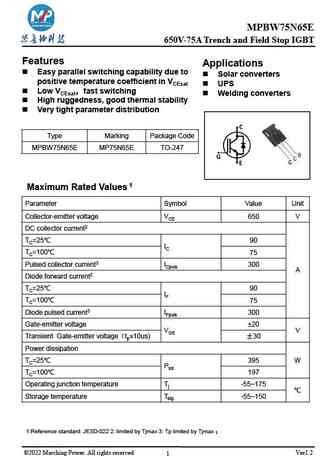
MPBW75N65E 650V-75A Trench and Field Stop IGBT Features Applications Easy parallel switching capability due to Solar converters positive temperature coefficient in VCEsat UPS Low VCEsat fast switching Welding converters High ruggedness, good thermal stability Very tight parameter distribution Type Marking Package Code MPBW75N65E MP75N65E TO-247 1 Max
spd15n65t1.pdf
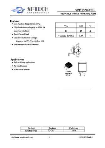
SPD15N65T1 650V /15A Trench Field Stop IGBT Features Max Junction Temperature 150 C V 650 V CE High breakdown voltage up to 650V for improved reliability I 15 A C Short Circuit Rated V I =15A 1.65 V CE(SAT) C Very Low Saturation Voltage V = 1.65V (Typ.) @ I = 15A CE(SAT) C Soft current turn-off waveforms Applications Soft switching application
spt15n65t1.pdf
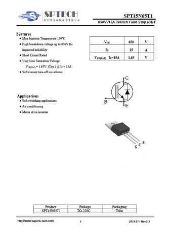
SPT15N65T1 650V /15A Trench Field Stop IGBT Features Max Junction Temperature 150 C V 650 V CE High breakdown voltage up to 650V for improved reliability I 15 A C Short Circuit Rated V I =15A 1.65 V CE(SAT) C Very Low Saturation Voltage V = 1.65V (Typ.) @ I = 15A CE(SAT) C Soft current turn-off waveforms Applications Soft switching application
ygw75n65f1.pdf
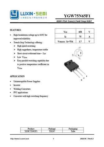
YGW75N65F1 650V /75A Trench Field Stop IGBT FEATURES V 650 V CE High breakdown voltage up to 650V for I 75 A C improved reliability V I =75A 1.7 V CE(SAT) C Trench-Stop Technology offering High speed switching High ruggedness, temperature stable Short circuit withstand time 5 s Low V CEsat Easy parallel switching capability due
ygw75n65fp.pdf
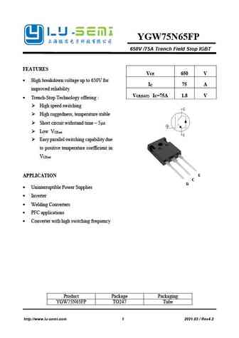
YGW75N65FP 650V /75A Trench Field Stop IGBT FEATURES V 650 V CE High breakdown voltage up to 650V for I 75 A C improved reliability V I =75A 1.8 V CE(SAT) C Trench-Stop Technology offering High speed switching High ruggedness, temperature stable Short circuit withstand time 5 s Low V CEsat Easy parallel switching capability due
ygf15n65t2 ygk15n65t2 ygp15n65t2.pdf
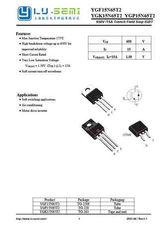
YGF15N65T2 YGK15N65T2 YGP15N65T2 650V /15A Trench Field Stop IGBT Features Max Junction Temperature 175 C V 650 V CE High breakdown voltage up to 650V for improved reliability I 15 A C Short Circuit Rated V I =15A 1.50 V CE(SAT) C Very Low Saturation Voltage V = 1.50V (Typ.) @ I = 15A CE(SAT) C Soft current turn-off waveforms Applications
ygw75n65hp.pdf
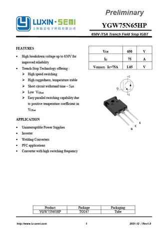
Preliminary YGW75N65HP 650V /75A Trench Field Stop IGBT FEATURES V 650 V CE High breakdown voltage up to 650V for I 75 A C improved reliability V I =75A 1.65 V CE(SAT) C Trench-Stop Technology offering High speed switching High ruggedness, temperature stable Short circuit withstand time 5 s Low V CEsat Easy parallel switching c
ygw75n65t1.pdf
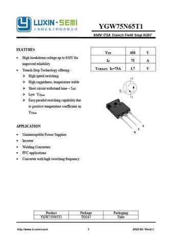
YGW75N65T1 650V /75A Trench Field Stop IGBT FEATURES V 650 V CE High breakdown voltage up to 650V for I 75 A C improved reliability V I =75A 1.7 V CE(SAT) C Trench-Stop Technology offering High speed switching High ruggedness, temperature stable Short circuit withstand time 5 s Low V CEsat Easy parallel switching capability due
augs65n65fpa5.pdf
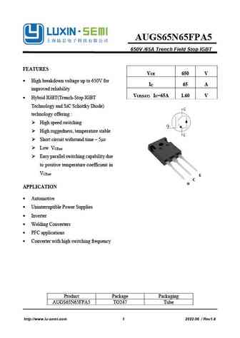
AUGS65N65FPA5 650V /65A Trench Field Stop IGBT FEATURES V 650 V CE High breakdown voltage up to 650V for I 65 A C improved reliability V I =65A 1.60 V CE(SAT) C Hybrid IGBT(Trench-Stop IGBT Technology and SiC Schottky Diode) technology offering High speed switching High ruggedness, temperature stable Short circuit withstand time 5 s
hckd5n65bm2.pdf
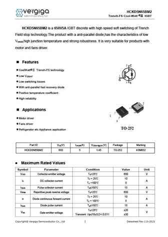
HCKD5N65BM2 @ Trench-FS Cool-Watt IGBT HCKD5N65BM2 is a 650V5A IGBT discrete with high speed soft switching of Trench Field stop technology.The product with a anti-parallel diode,has the characteristics of low V ,high junction temperature and strong robustness. It is very suitable for products with cesat motor and fans driver. Features CoolWatt@ Trench-FS technology
hckw75n65gh2.pdf
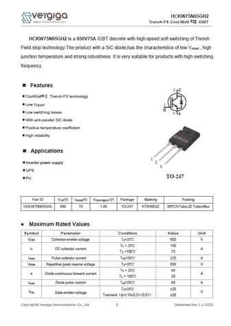
HCKW75N65GH2 @ Trench-FS Cool-Watt IGBT HCKW75N65GH2 is a 650V75A IGBT discrete with high speed soft switching of Trench Field stop technology.The product with a SiC diode,has the characteristics of low V , high cesat junction temperature and strong robustness. It is very suitable for products with high switching frequency. Features CoolWatt@ Trench-FS technology Lo
hckz75n65bh2.pdf
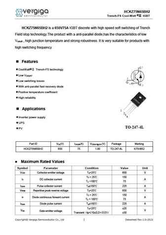
HCKZ75N65BH2 @ Trench-FS Cool-Watt IGBT HCKZ75N65BH2 is a 650V75A IGBT discrete with high speed soft switching of Trench Field stop technology.The product with a anti-parallel diode,has the characteristics of low V , high junction temperature and strong robustness. It is very suitable for products with cesat high switching frequency. Features CoolWatt@ Trench-FS technolo
hckz75n65gh2.pdf
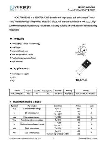
HCKZ75N65GH2 @ Trench-FS Cool-Watt IGBT HCKZ75N65GH2 is a 650V75A IGBT discrete with high speed soft switching of Trench Field stop technology.The product with a SiC diode,has the characteristics of low V , high cesat junction temperature and strong robustness. It is very suitable for products with high switching frequency. Features CoolWatt@ Trench-FS technology Lo
hckd5n65am2.pdf
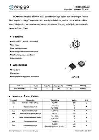
HCKD5N65AM2 @ Trench-FS Cool-Watt IGBT HCKD5N65AM2 is a 650V5A IGBT discrete with high speed soft switching of Trench Field stop technology.The product with a anti-parallel diode,has the characteristics of low V ,high junction temperature and strong robustness. It is very suitable for products with cesat motor and fans driver. Features CoolWatt@ Trench-FS technology
hckw75n65fh2.pdf
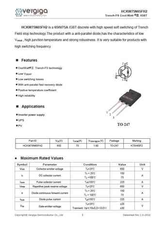
HCKW75N65FH2 @ Trench-FS Cool-Watt IGBT HCKW75N65FH2 is a 650V75A IGBT discrete with high speed soft switching of Trench Field stop technology.The product with a anti-parallel diode,has the characteristics of low V , high junction temperature and strong robustness. It is very suitable for products with cesat high switching frequency. Features CoolWatt@ Trench-FS technolo
hckw75n65bh2.pdf
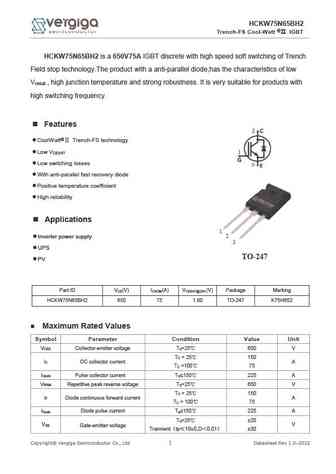
HCKW75N65BH2 @ Trench-FS Cool-Watt IGBT HCKW75N65BH2 is a 650V75A IGBT discrete with high speed soft switching of Trench Field stop technology.The product with a anti-parallel diode,has the characteristics of low V , high junction temperature and strong robustness. It is very suitable for products with cesat high switching frequency. Features CoolWatt@ Trench-FS technolo
stf45n65m5.pdf
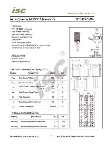
isc N-Channel MOSFET Transistor STF45N65M5 FEATURES With TO-220F packaging High speed switching Low gate input resistance Standard level gate drive Easy to use 100% avalanche tested Minimum Lot-to-Lot variations for robust device performance and reliable operation APPLICATIONS Power supply Switching applications ABSOLUTE MAXIMUM RATINGS(T =25 ) a SYMBOL
stwa45n65m5.pdf
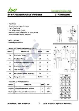
INCHANGE Semiconductor Isc N-Channel MOSFET Transistor STWA45N65M5 FEATURES Excellent switching performance Higher V rating DSS 100 % Rg and UIS Tested Minimum Lot-to-Lot variations for robust device performance and reliable operation APPLICATIONS Switching applications ABSOLUTE MAXIMUM RATINGS(T =25 ) a SYMBOL PARAMETER VALUE UNIT V Drain-Source Voltage 650 V D
5n65k.pdf
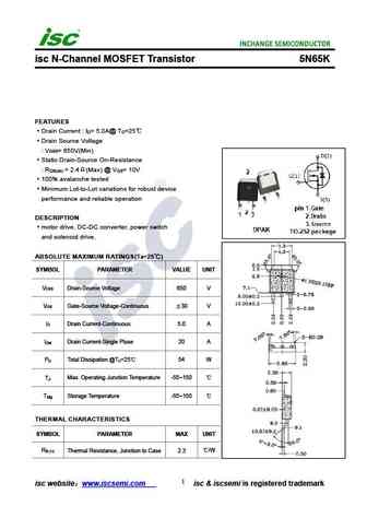
isc N-Channel MOSFET Transistor 5N65K FEATURES Drain Current I = 5.0A@ T =25 D C Drain Source Voltage V = 650V(Min) DSS Static Drain-Source On-Resistance R = 2.4 (Max) @ V = 10V DS(on) GS 100% avalanche tested Minimum Lot-to-Lot variations for robust device performance and reliable operation DESCRIPTION motor drive, DC-DC converter, power switch and solenoid
fcp125n65s3.pdf
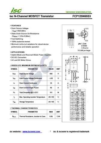
isc N-Channel MOSFET Transistor FCP125N65S3 FEATURES Drain Source Voltage- V = 650V(Min) DSS Static Drain-Source On-Resistance R = 125m (Max) DS(on) Fast Switching 100% avalanche tested Minimum Lot-to-Lot variations for robust device performance and reliable operation APPLICATIONS Switch-Mode and Resonant-Mode Power Supplies DC-DC Converters AC and DC Mot
stp45n65m5.pdf
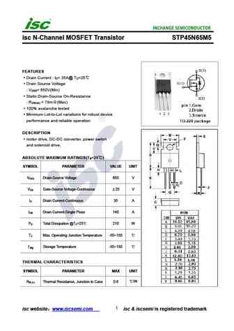
isc N-Channel MOSFET Transistor STP45N65M5 FEATURES Drain Current I = 35A@ T =25 D C Drain Source Voltage V = 650V(Min) DSS Static Drain-Source On-Resistance R = 78m (Max) DS(on) 100% avalanche tested Minimum Lot-to-Lot variations for robust device performance and reliable operation DESCRIPTION motor drive, DC-DC converter, power switch and solenoid drive.
fcp125n65s.pdf
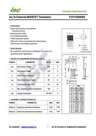
isc N-Channel MOSFET Transistor FCP125N65S FEATURES Static drain-source on-resistance RDS(on) 2.3m Enhancement mode Fast Switching Speed 100% avalanche tested Minimum Lot-to-Lot variations for robust device performance and reliable operation DESCRITION Be suitable for synchronous rectification for server and general purpose applications ABSOLUTE MAXIMUM RATI
stb45n65m5.pdf
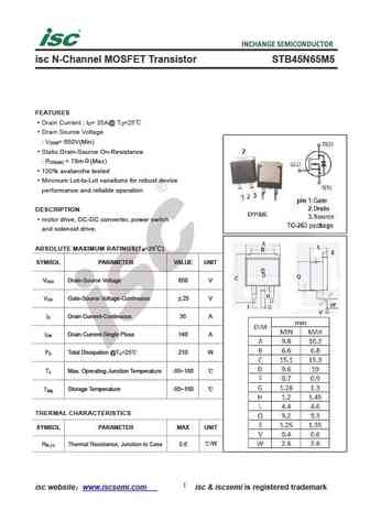
isc N-Channel MOSFET Transistor STB45N65M5 FEATURES Drain Current I = 35A@ T =25 D C Drain Source Voltage V = 650V(Min) DSS Static Drain-Source On-Resistance R = 78m (Max) DS(on) 100% avalanche tested Minimum Lot-to-Lot variations for robust device performance and reliable operation DESCRIPTION motor drive, DC-DC converter, power switch and solenoid drive.
stfw45n65m5.pdf
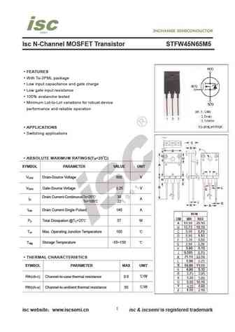
Isc N-Channel MOSFET Transistor STFW45N65M5 FEATURES With To-3PML package Low input capacitance and gate charge Low gate input resistance 100% avalanche tested Minimum Lot-to-Lot variations for robust device performance and reliable operation APPLICATIONS Switching applications ABSOLUTE MAXIMUM RATINGS(T =25 ) a SYMBOL PARAMETER VALUE UNIT V Drain-Source Voltage
irfib5n65a.pdf
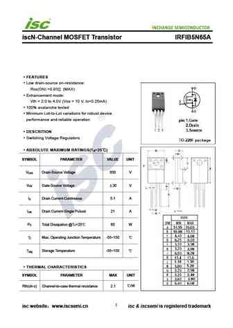
iscN-Channel MOSFET Transistor IRFIB5N65A FEATURES Low drain-source on-resistance RDS(ON) =0.93 (MAX) Enhancement mode Vth = 2.0 to 4.0V (VDS = 10 V, ID=0.25mA) 100% avalanche tested Minimum Lot-to-Lot variations for robust device performance and reliable operation DESCRITION Switching Voltage Regulators ABSOLUTE MAXIMUM RATINGS(T =25 ) a SYMBOL PARAMETER VAL
15n65.pdf
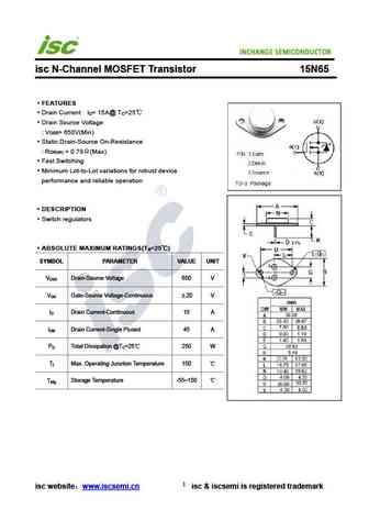
isc N-Channel MOSFET Transistor 15N65 FEATURES Drain Current I = 15A@ T =25 D C Drain Source Voltage V = 650V(Min) DSS Static Drain-Source On-Resistance R = 0.78 (Max) DS(on) Fast Switching Minimum Lot-to-Lot variations for robust device performance and reliable operation DESCRIPTION Switch regulators ABSOLUTE MAXIMUM RATINGS(T =25 ) a SYMBOL PARAMET
spa15n65c3.pdf
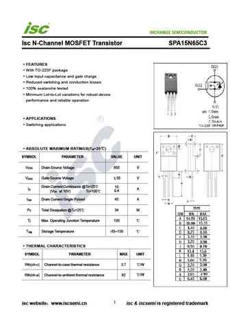
INCHANGE Semiconductor Isc N-Channel MOSFET Transistor SPA15N65C3 FEATURES With TO-220F package Low input capacitance and gate charge Reduced switching and conduction losses 100% avalanche tested Minimum Lot-to-Lot variations for robust device performance and reliable operation APPLICATIONS Switching applications ABSOLUTE MAXIMUM RATINGS(T =25 ) a SYMBOL PARAMET
wfd5n65l.pdf
Isc N-Channel MOSFET Transistor WFD5N65L FEATURES With To-252(DPAK) package Low input capacitance and gate charge Low gate input resistance 100% avalanche tested Minimum Lot-to-Lot variations for robust device performance and reliable operation APPLICATIONS Switching applications ABSOLUTE MAXIMUM RATINGS(T =25 ) a SYMBOL PARAMETER VALUE UNIT V Drain-Source Volta
stb35n65m5.pdf
INCHANGE Semiconductor isc N-Channel MOSFET Transistor STB35N65M5 FEATURES With TO-263( D2PAK ) packaging High speed switching Low gate input resistance Standard level gate drive Easy to use 100% avalanche tested Minimum Lot-to-Lot variations for robust device performance and reliable operation APPLICATIONS Power supply Switching applications ABSOLUTE MAXIM
fcpf165n65s3l1.pdf
isc N-Channel MOSFET Transistor FCPF165N65S3L1 FEATURES With TO-220F packaging High speed switching Low gate input resistance Standard level gate drive Easy to use 100% avalanche tested Minimum Lot-to-Lot variations for robust device performance and reliable operation APPLICATIONS Power supply Switching applications ABSOLUTE MAXIMUM RATINGS(T =25 ) a SYM
fcpf125n65s3.pdf
INCHANGE Semiconductor Isc N-Channel MOSFET Transistor FCPF125N65S3 FEATURES With To-220F package Low input capacitance and gate charge Low gate input resistance 100% avalanche tested Minimum Lot-to-Lot variations for robust device performance and reliable operation APPLICATIONS Switching applications ABSOLUTE MAXIMUM RATINGS(T =25 ) a SYMBOL PARAMETER VALUE UNI
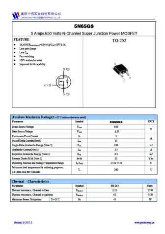
Otros transistores... 2N65K, 3N65A, 3N65, 3N65Z, 3N65K, 4N65, 4N65Z, 4N65K, IRL3713, 5N65K, 6N65, 5N60, 6N60, 6N60Z, 7N60A, 7N60, 7N60Z
Parámetros del MOSFET. Cómo se afectan entre sí.
🌐 : EN ES РУ

Liste
Recientemente añadidas las descripciónes de los transistores:
MOSFET: BC3134KT | BC3134K | BC2302W | BC2302T-2.8A | BC2302-2.8A | BC2301W | BC2301T-2.8A | CB3139KTB | CB2301DW | BC8205 | BC3415 | BC3407 | BC3401 | BC3400 | BC2301 | BC1012W
Popular searches
2n5457 | k3568 | 2sc1344 | cs840f | 2n3053 equivalent | 2n3569 | 2sd667 | 2sc1111