6N65 MOSFET Equivalente. Reemplazo. Hoja de especificaciones. Principales características
Número de Parte: 6N65
Tipo de FET: MOSFET
Polaridad de transistor: N
ESPECIFICACIONES MÁXIMAS
Pdⓘ - Máxima disipación de potencia: 125 W
|Vds|ⓘ - Voltaje máximo drenador-fuente: 650 V
|Vgs|ⓘ - Voltaje máximo fuente-puerta: 30 V
|Id|ⓘ - Corriente continua de drenaje: 6.2 A
Tjⓘ - Temperatura máxima de unión: 150 °C
CARACTERÍSTICAS ELÉCTRICAS
trⓘ - Tiempo de subida: 100 nS
Cossⓘ - Capacitancia de salida: 95 pF
RDSonⓘ - Resistencia estado encendido drenaje a fuente: 1.1 Ohm
Encapsulados: TO-220 TO-251 TO-252 TO-220F TO-220F1
Búsqueda de reemplazo de 6N65 MOSFET
- Selecciónⓘ de transistores por parámetros
6N65 datasheet
6n65.pdf
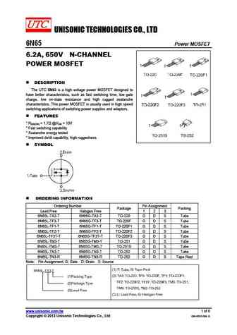
UNISONIC TECHNOLOGIES CO., LTD 6N65 Power MOSFET 6.2A, 650V N-CHANNEL POWER MOSFET DESCRIPTION The UTC 6N65 is a high voltage power MOSFET designed to have better characteristics, such as fast switching time, low gate charge, low on-state resistance and high rugged avalanche characteristics. This power MOSFET is usually used in high speed switching applications of switchin
6n65 6n65f 6n65d.pdf
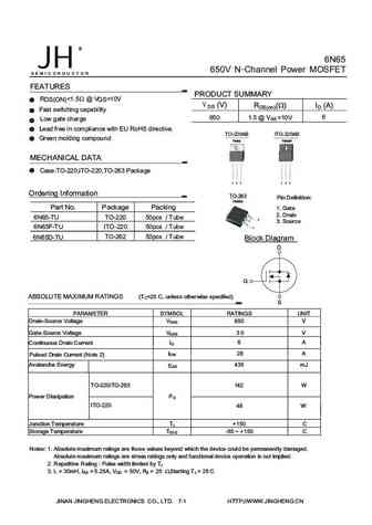
6N65 JH 650V N-Channel Power MOSFET S E M I C O N D U C T O R FEATURES PRODUCT SUMMARY RDS(ON)
stp16n65m5 stu16n65m5 stw16n65m5 sti16n65m5 stf16n65m5.pdf

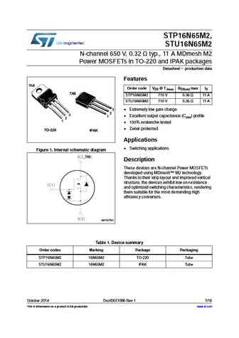
STF16N65M5, STI16N65M5 STP16N65M5,STU16N65M5,STW16N65M5 N-channel 650 V, 0.240 , 12 A MDmesh V Power MOSFET in TO-220FP, TO-220, IPAK, I2PAK, TO-247 Features VDSS @ RDS(on) Type ID TJmax max 3 3 3 2 2 2 1 STF16N65M5 1 1 TO-220 STI16N65M5 TO-247 TO-220FP STP16N65M5 710 V
stl16n65m2.pdf
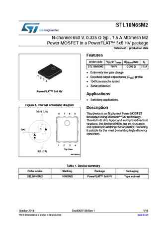
STL16N65M2 N-channel 650 V, 0.325 typ., 7.5 A MDmesh M2 Power MOSFET in a PowerFLAT 5x6 HV package Datasheet - production data Features Order code VDS @ TJmax RDS(on) max ID STL16N65M2 710 V 0.395 7.5 A Extremely low gate charge 1 Excellent output capacitance (Coss) profile 2 3 4 100% avalanche tested Zener-protected PowerFLAT 5x6 HV Applications
stf16n65m5 sti16n65m5 stp16n65m5 stu16n65m5 stw16n65m5.pdf
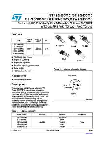
STF16N65M5, STI16N65M5 STP16N65M5,STU16N65M5,STW16N65M5 N-channel 650 V, 0.230 , 12 A MDmesh V Power MOSFET in TO-220FP, I PAK, TO-220, IPAK, TO-247 Features TAB TAB VDSS @ RDS(on) Type ID TJmax max 3 2 3 3 2 1 1 2 STF16N65M5 1 TO-220FP TO-220 STI16N65M5 I PAK STP16N65M5 710 V
stw56n65dm2.pdf
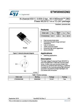
STW56N65DM2 N-channel 650 V, 0.058 typ., 48 A MDmesh DM2 Power MOSFET in a TO-247 package Datasheet - production data Features R DS(on) Order code V I P DS D TOT max. STW56N65DM2 650 V 0.065 48 A 360 W Fast-recovery body diode 3 Extremely low gate charge and input 2 capacitance 1 Low on-resistance 100% avalanche tested TO-247 Extre
stf6n65m2 stp6n65m2 stu6n65m2.pdf
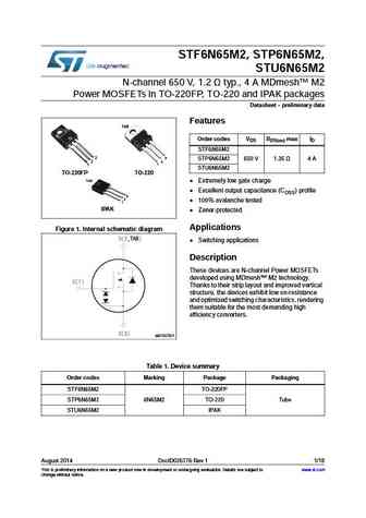
STF6N65M2, STP6N65M2, STU6N65M2 N-channel 650 V, 1.2 typ., 4 A MDmesh M2 Power MOSFETs in TO-220FP, TO-220 and IPAK packages Datasheet - preliminary data Features TAB Order codes VDS RDS(on) max ID STF6N65M2 3 3 STP6N65M2 650 V 1.35 4 A 2 2 1 1 STU6N65M2 TO-220FP TO-220 TAB Extremely low gate charge Excellent output capacitance (COSS) profile 3 2 1
stw56n65m2.pdf
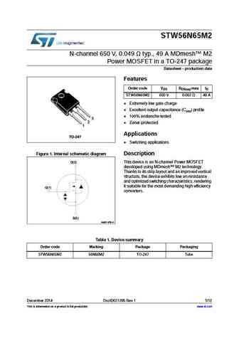
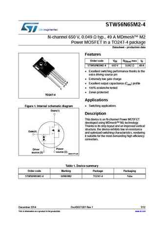
STW56N65M2 N-channel 650 V, 0.049 typ., 49 A MDmesh M2 Power MOSFET in a TO-247 package Datasheet - production data Features Order code VDS RDS(on) max ID STW56N65M2 650 V 0.062 49 A Extremely low gate charge Excellent output capacitance (Coss) profile 100% avalanche tested 3 2 Zener-protected 1 Applications TO-247 Switching applications Figure
stl16n65m5.pdf
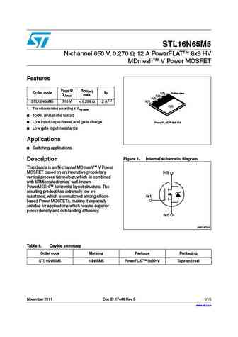
STL16N65M5 N-channel 650 V, 0.270 , 12 A PowerFLAT 8x8 HV MDmesh V Power MOSFET Features VDSS @ RDS(on) Order code ID S(2) Bottom view TJmax max S(2) S(2) G(1) STL16N65M5 710 V
stf6n65k3 stfi6n65k3 stu6n65k3.pdf

STF6N65K3, STFI6N65K3, STU6N65K3 N-channel 650 V, 1.1 typ., 5.4 A SuperMESH3 Power MOSFET in TO-220FP, I PAKFP, IPAK Datasheet production data Features Order codes VDSS RDS(on) max. ID Ptot STF6N65K3 TAB 30 W STFI6N65K3 650 V
std16n65m2.pdf
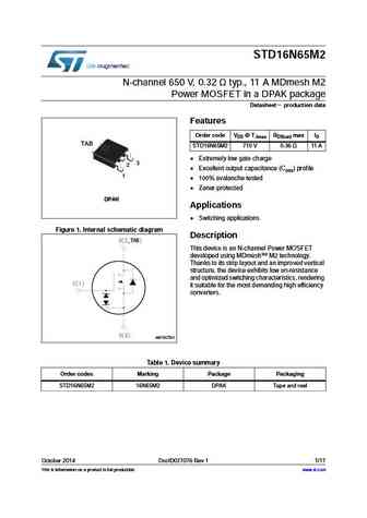
STD16N65M2 N-channel 650 V, 0.32 typ., 11 A MDmesh M2 Power MOSFET in a DPAK package Datasheet - production data Features Order code VDS @ TJmax RDS(on) max ID TAB STD16N65M2 710 V 0.36 11 A Extremely low gate charge 3 2 Excellent output capacitance (Coss) profile 1 100% avalanche tested Zener-protected DPAK Applications Switching applications Fig
stfi6n65k3 stu6n65k3.pdf
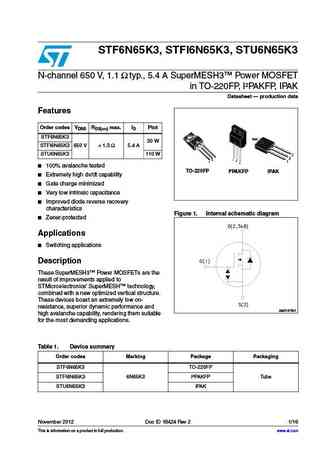
STF6N65K3, STFI6N65K3, STU6N65K3 N-channel 650 V, 1.1 typ., 5.4 A SuperMESH3 Power MOSFET in TO-220FP, I PAKFP, IPAK Datasheet production data Features Order codes VDSS RDS(on) max. ID Ptot STF6N65K3 TAB 30 W STFI6N65K3 650 V
stb6n65m2 std6n65m2.pdf
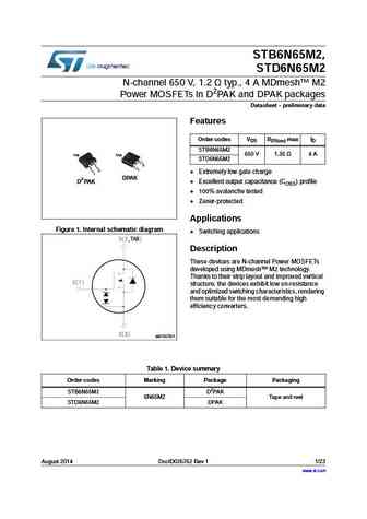
STB6N65M2, STD6N65M2 N-channel 650 V, 1.2 typ., 4 A MDmesh M2 Power MOSFETs in D2PAK and DPAK packages Datasheet - preliminary data Features Order codes VDS RDS(on) max ID STB6N65M2 650 V 1.35 4 A TAB TAB STD6N65M2 3 1 3 Extremely low gate charge 1 DPAK 2 D PAK Excellent output capacitance (COSS) profile 100% avalanche tested Zener-protected App
std16n65m5.pdf
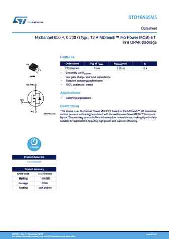
STD16N65M5 Datasheet N-channel 650 V, 0.230 typ., 12 A MDmesh M5 Power MOSFET in a DPAK package Features VDS at Tjmax. RDS(on) max. ID Order codes TAB STD16N65M5 710 V 0.279 12 A 3 2 1 Extremely low RDS(on) DPAK Low gate charge and input capacitance Excellent switching performance D(2, TAB) 100% avalanche tested Applications Switching applications
stp26n65dm2.pdf
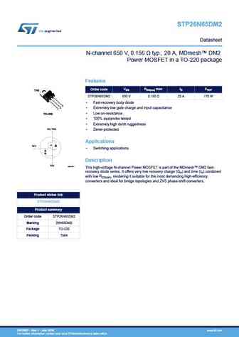
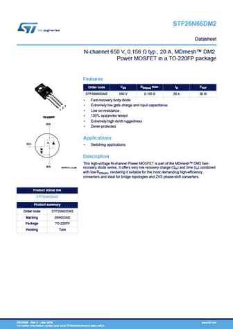
STP26N65DM2 Datasheet N-channel 650 V, 0.156 typ., 20 A, MDmesh DM2 Power MOSFET in a TO-220 package Features VDS RDS(on) max. ID PTOT Order code TAB STP26N65DM2 650 V 0.190 20 A 170 W Fast-recovery body diode 3 2 Extremely low gate charge and input capacitance 1 Low on-resistance TO-220 100% avalanche tested Extremely high dv/dt ruggedness D(2, T
stw56n65m2-4.pdf
STW56N65M2-4 N-channel 650 V, 0.049 typ., 49 A MDmesh M2 Power MOSFET in a TO247-4 package Datasheet - production data Features Order code VDS RDS(on) max ID STW56N65M2-4 650 V 0.062 49 A Excellent switching performance thanks to the extra driving source pin Extremely low gate charge 4 Excellent output capacitance (Coss) profile 3 2 100% avalanche tes
stf16n65m2.pdf
STF16N65M2 N-channel 650 V, 0.32 typ., 11 A MDmesh M2 Power MOSFET in a TO-220FP package Datasheet - production data Features Order code VDS @ TJmax RDS(on) max ID STF16N65M2 710 V 0.36 11 A Extremely low gate charge Excellent output capacitance (Coss) profile 100% avalanche tested Zener-protected Applications TO-220FP Switching applications Figure 1.
stfu16n65m2.pdf
STFU16N65M2 N-channel 650 V, 0.32 typ., 11 A MDmesh M2 Power MOSFET in a TO-220FP ultra narrow leads package Datasheet - production data Features Order code V R max I DS DS(on) D STFU16N65M2 650 V 0.36 11 A Extremely low gate charge Excellent output capacitance (C ) profile OSS 100% avalanche tested 3 2 1 Zener-protected TO-220FP Applications
stb16n65m5 std16n65m5.pdf
STB16N65M5 STD16N65M5 N-channel 650 V, 0.270 , 12 A MDmesh V Power MOSFET in D PAK, DPAK Features VDSS @ RDS(on) Type ID TJmax max. STB16N65M5 710 V
stp16n65m5 stu16n65m5 stw16n65m5 sti16n65m5 stf16n65m5 2.pdf
STF16N65M5, STI16N65M5 STP16N65M5,STU16N65M5,STW16N65M5 N-channel 650 V, 0.270 , 12 A MDmesh V Power MOSFET in TO-220FP, TO-220, IPAK, I2PAK, TO-247 Features VDSS @ RDS(on) Type ID TJmax max 3 3 3 2 2 2 1 STF16N65M5 1 1 TO-220 STI16N65M5 TO-247 TO-220FP STP16N65M5 710 V
sihp6n65e.pdf

SiHP6N65E www.vishay.com Vishay Siliconix E Series Power MOSFET FEATURES PRODUCT SUMMARY Low figure-of-merit (FOM) Ron x Qg VDS (V) at TJ max. 700 Low input capacitance (Ciss) RDS(on) max. at 25 C ( ) VGS = 10 V 0.6 Reduced switching and conduction losses Qg max. (nC) 48 Ultra low gate charge (Qg) Qgs (nC) 6 Avalanche energy rated (UIS) Qgd (nC) 11 Mat
sihb6n65e.pdf
SiHB6N65E www.vishay.com Vishay Siliconix E Series Power MOSFET FEATURES PRODUCT SUMMARY Low figure-of-merit (FOM) Ron x Qg VDS (V) at TJ max. 700 Low input capacitance (Ciss) RDS(on) max. at 25 C ( ) VGS = 10 V 0.6 Reduced switching and conduction losses Qg max. (nC) 48 Ultra low gate charge (Qg) Qgs (nC) 6 Avalanche energy rated (UIS) Qgd (nC) 11 Mat
sihu6n65e.pdf
SiHU6N65E www.vishay.com Vishay Siliconix E Series Power MOSFET FEATURES PRODUCT SUMMARY Low figure-of-merit (FOM) Ron x Qg VDS (V) at TJ max. 700 Low input capacitance (Ciss) RDS(on) max. at 25 C ( ) VGS = 10 V 0.6 Reduced switching and conduction losses Qg max. (nC) 48 Ultra low gate charge (Qg) Qgs (nC) 6 Avalanche energy rated (UIS) Qgd (nC) 11 Mat
sihd6n65e.pdf
SiHD6N65E www.vishay.com Vishay Siliconix E Series Power MOSFET FEATURES PRODUCT SUMMARY Low figure-of-merit (FOM) Ron x Qg VDS (V) at TJ max. 700 Low input capacitance (Ciss) RDS(on) max. at 25 C ( ) VGS = 10 V 0.6 Reduced switching and conduction losses Qg max. (nC) 48 Ultra low gate charge (Qg) Qgs (nC) 6 Avalanche energy rated (UIS) Qgd (nC) 11 Mat
sihf6n65e.pdf
SiHF6N65E www.vishay.com Vishay Siliconix E Series Power MOSFET FEATURES PRODUCT SUMMARY Low figure-of-merit (FOM) Ron x Qg VDS (V) at TJ max. 700 Low input capacitance (Ciss) RDS(on) max. at 25 C ( ) VGS = 10 V 0.6 Reduced switching and conduction losses Qg max. (nC) 48 Ultra low gate charge (Qg) Qgs (nC) 6 Avalanche energy rated (UIS) Qgd (nC) 11 Mat
ixfh46n65x2.pdf
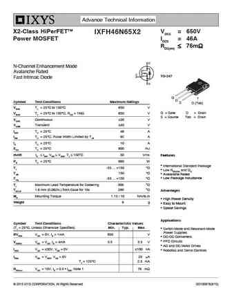
Advance Technical Information X2-Class HiPerFETTM VDSS = 650V IXFH46N65X2 Power MOSFET ID25 = 46A RDS(on) 76m N-Channel Enhancement Mode Avalanche Rated TO-247 Fast Intrinsic Diode G D Symbol Test Conditions Maximum Ratings S D (Tab) VDSS TJ = 25 C to 150 C 650 V G = Gate D = Drain VDGR TJ = 25 C to 150 C, RGS = 1M 650 V S =
6n65kl-tms-t 6n65kg-tms-t 6n65kl-tms2-t 6n65kg-tms2-t 6n65kl-tms4-t 6n65kg-tms4-t 6n65kl-tn3-r 6n65kg-tn3-r 6n65kl-tnd-r 6n65kg-tnd-r.pdf

UNISONIC TECHNOLOGIES CO., LTD 6N65K-MT Power MOSFET 6A, 650V N-CHANNEL POWER MOSFET DESCRIPTION The UTC 6N65K-MT is a high voltage power MOSFET designed to have better characteristics, such as fast switching time, low gate charge, low on-state resistance and high rugged avalanche characteristics. This power MOSFET is usually used in high speed switching applications of swi
6n65z.pdf
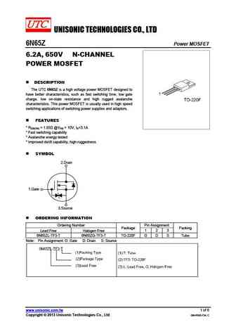
UNISONIC TECHNOLOGIES CO., LTD 6N65Z Power MOSFET 6.2A, 650V N-CHANNEL POWER MOSFET DESCRIPTION The UTC 6N65Z is a high voltage power MOSFET designed to have better characteristics, such as fast switching time, low gate charge, low on-state resistance and high rugged avalanche characteristics. This power MOSFET is usually used in high speed switching applications of switch
6n65kl-ta3-t 6n65kg-ta3-t 6n65kl-tf3-t 6n65kg-tf3-t 6n65kl-tf1-t 6n65kg-tf1-t 6n65kl-tf2-t 6n65kg-tf2-t 6n65kl-tf3-t 6n65kg-tf3-t 6n65kl-tm3-t 6n65kg-tm3-t.pdf
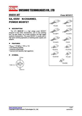
UNISONIC TECHNOLOGIES CO., LTD 6N65K-MT Power MOSFET 6A, 650V N-CHANNEL POWER MOSFET DESCRIPTION The UTC 6N65K-MT is a high voltage power MOSFET designed to have better characteristics, such as fast switching time, low gate charge, low on-state resistance and high rugged avalanche characteristics. This power MOSFET is usually used in high speed switching applications of swi
mtn6n65fp.pdf
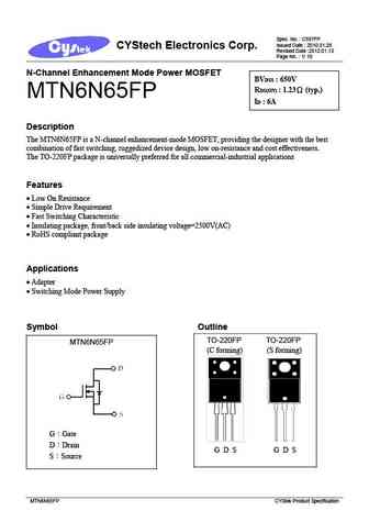
Spec. No. C597FP Issued Date 2010.01.28 CYStech Electronics Corp. Revised Date 2012.01.13 Page No. 1/ 10 N-Channel Enhancement Mode Power MOSFET BVDSS 650V RDS(ON) 1.23 (typ.) MTN6N65FP ID 6A Description The MTN6N65FP is a N-channel enhancement-mode MOSFET, providing the designer with the best combination of fast switching, ruggedized device design, low on-
ftp06n65 fta06n65.pdf
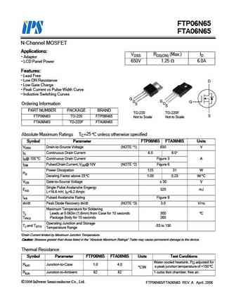
FTP06N65 FTA06N65 N-Channel MOSFET Applications VDSS RDS(ON) (Max.) ID Adaptor 650V 1.25 6.0A LCD Panel Power Features Lead Free Low ON Resistance D Low Gate Charge Peak Current vs Pulse Width Curve Inductive Switching Curves G G D G Ordering Information S D S PART NUMBER PACKAGE BRAND TO-220 TO-220F S FTP06N65 TO-220 FTP06N65 Not to Sc
f16n65.pdf
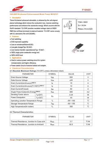
F16N65 16A 650V N-channel Enhancement Mode Power MOSFET 1 Description These N-channel enhanced vdmosfets, is obtained by the self-aligned V DSS = 650V planar technology which reduce the conduction loss, improve switching I = 16.0A D performance and enhance the avalanche energy. Which accords with the RoHS standard. TO-220F provides insulation voltage rated at 2000V R DS(on) TYP)
ndt6n65p.pdf
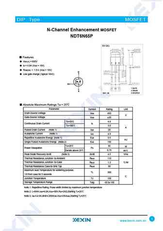
DIP Type MOSFET N-Channel Enhancement MOSFET NDT6N65P TO-251 Features VDS (V) = 650V 1 2 3 ID = 4.8A (VGS = 10V) RDS(ON) 1.8 (VGS = 10V) D Low gate charge ( typical 16nC) 1 3 2 G S Unit mm Absolute Maximum Ratings Ta = 25 Parameter Symbol Rating Unit Drain-Source Voltage VDS 650 V Gate-Source Voltage VGS 30 Tc=25 4.8 Continuou
mdf6n65bth.pdf
MDF6N65B N-Channel MOSFET 650V, 6.0A, 1.45 General Description Features The MDF6N65B use advanced Magnachip s VDS = 650V MOSFET Technology, which provides low on-state @VGS = 10V ID = 6.0A resistance, high switching performance and @VGS = 10V RDS(ON) 1.45 excellent quality. MDF6N65B is suitable device for SMPS, HID and general purpose applications. Applications
mdi6n65bth.pdf
MDI6N65B N-Channel MOSFET 650V, 5.7A, 1.45 General Description Features The MDI6N65B use advanced Magnachip s VDS = 650V MOSFET Technology, which provides low on-state ID = 5.7A @VGS = 10V resistance, high switching performance and RDS(ON) 1.45 @VGS = 10V excellent quality. MDI6N65B is suitable device for SMPS, HID and general purpose applications. Applicat
msf6n65.pdf
MSF6N65 N-Channel Enhancement Mode Power MOSFET Description The MSF6N65 is a N-channel enhancement-mode MOSFET , providing the designer with the best combination of fast switching, ruggedized device design, low on-resistance and cost effectiveness. The TO-220F package is universally preferred for all commercial-industrial applications Features Low On Resistance Sim
slf16n65s.pdf
SLF16N65S 650V N-Channel MOSFET General Description Features This Power MOSFET is produced using Msemitek s advanced 16A*, 650V, RDS(on),typ =0.42 planar stripe DMOS technology. This advanced technology Low gate charge (Qg,typ = 37nC) has been especially tailored to minimize conduction loss, pro- Fast switching vide superior switching performance, and withstand high en-
ptp16n65 pta16n65.pdf
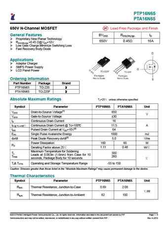
PTP16N65 PTA16N65 650V N-Channel MOSFET General Features BVDSS RDS(ON),typ. ID Proprietary New Planar Technology 650V 0.45 16A RDS(ON),typ.=0.45 @VGS=10V Low Gate Charge Minimize Switching Loss Fast Recovery Body Diode Applications Adaptor Charger SMPS Power Supply LCD Panel Power Ordering Information Part Number Package Brand PTP16N65 TO-220 PTA16N
pta26n65.pdf
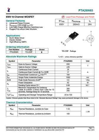
PTA26N65 650V N-Channel MOSFET General Features BVDSS RDS(ON),typ. ID Advanced Planar Process 650V 280m 26A RDS(ON),typ.=280 m @VGS=10V Low Gate Charge Minimize Switching Loss Rugged Poly silicon Gate Structure Applications BLDC Motor Driver Electric Welder High Efficiency SMPS G D S Ordering Information Part Number Package Brand TO-220F Package
sw16n65d swf16n65d.pdf
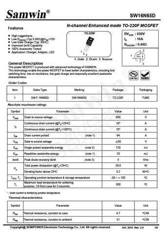
SW16N65D N-channel Enhanced mode TO-220F MOSFET Features TO-220F BVDSS 650V High ruggedness Low RDS(ON) (Typ 0.46 )@VGS=10V ID 16A Low Gate Charge (Typ 68nC) RDS(ON) 0.46 Improved dv/dt Capability 100% Avalanche Tested 2 1 Application Charger, Adaptor, LED 2 3 1 1. Gate 2. Drain 3. Source General Description 3 This power MOSFET is produce
swf6n65k swi6n65k swn6n65k swd6n65k swu6n65k swmn6n65k.pdf
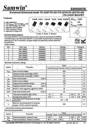
SW6N65K N-channel Enhanced mode TO-220F/TO-251/TO-251N/TO-252/TO-262 /TO-220SF MOSFET Features TO251 TO220F TO251N TO252 TO262 TO220SF BVDSS 650V High ruggedness ID 6A Low RDS(ON) (Typ 0.8 )@VGS=10V RDS(ON) 0.8 Low Gate Charge (Typ 17nC) Improved dv/dt Capability 2 1 1 100% Avalanche Tested 1 1 1 1 2 2 2 2 2 2 3 3 Applicat
swd6n65d.pdf
SW6N65D N-channel Enhanced mode TO-252 MOSFET TO-252 BVDSS 650V Features ID 6A High ruggedness RDS(ON) 1.3 Low RDS(ON) (Typ 1.3 )@VGS=10V Low Gate Charge (Typ 22nC) 2 Improved dv/dt Capability 1 100% Avalanche Tested 2 1 3 Application LED , Charger 1. Gate 2. Drain 3. Source 3 General Description This power MOSFET is
sw16n65k swp16n65k swf16n65k swb16n65k.pdf
SW16N65K N-channel Enhanced mode TO-220/TO-220F/TO-263 MOSFET Features TO-220 TO-220F TO-263 BVDSS 650V ID 16A High ruggedness Low RDS(ON) (Typ 0.23 )@VGS=10V RDS(ON) 0.23 Low Gate Charge (Typ 43nC) Improved dv/dt Capability 2 100% Avalanche Tested 1 1 1 2 2 2 Application LED, Charge, PC Power 3 3 3 1. Gate 2. Drain 3. Source
swf16n65d.pdf

SW16N65D N-channel Enhanced mode TO-220F MOSFET Features TO-220F BVDSS 650V High ruggedness Low RDS(ON) (Typ 0.46 )@VGS=10V ID 16A Low Gate Charge (Typ 68nC) RDS(ON) 0.46 Improved dv/dt Capability 100% Avalanche Tested 2 1 Application Charger, Adaptor, LED 2 3 1 1. Gate 2. Drain 3. Source General Description 3 This power MOSFET is produce
swp16n65k swf16n65k swb16n65k.pdf

SW16N65K N-channel Enhanced mode TO-220/TO-220F/TO-263 MOSFET Features TO-220 TO-220F TO-263 BVDSS 650V ID 16A High ruggedness Low RDS(ON) (Typ 0.23 )@VGS=10V RDS(ON) 0.23 Low Gate Charge (Typ 43nC) Improved dv/dt Capability 2 100% Avalanche Tested 1 1 1 2 2 2 Application LED, Charger, PC Power 3 3 3 1. Gate 2. Drain 3. Source
hfp6n65u.pdf
July 2012 BVDSS = 650 V RDS(on) typ HFP6N65U ID = 6.0 A 650V N-Channel MOSFET TO-220 FEATURES Originative New Design Superior Avalanche Rugged Technology 1 2 3 Robust Gate Oxide Technology 1.Gate 2. Drain 3. Source Very Low Intrinsic Capacitances Excellent Switching Characteristics Unrivalled Gate Charge 16.0 nC (Typ.) Extended Safe Operating Area
hfd6n65u.pdf
Jan 2014 BVDSS = 650 V RDS(on) typ HFD6N65U / HFU6N65U ID = 4.8 A 650V N-Channel MOSFET D-PAK I-PAK FEATURES 2 1 Originative New Design 1 3 2 3 Superior Avalanche Rugged Technology HFD6N65U HFU6N65U Robust Gate Oxide Technology 1.Gate 2. Drain 3. Source Very Low Intrinsic Capacitances Excellent Switching Characteristics Unrivalled Gate Charge 16.0 nC
hfs6n65u.pdf
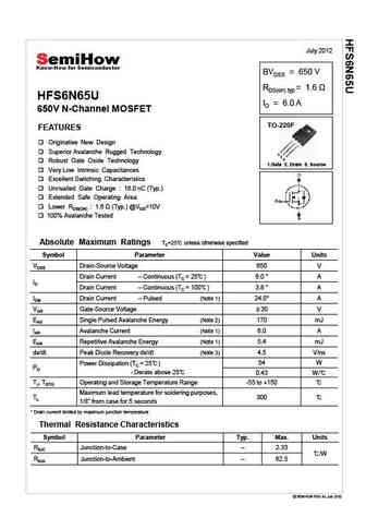
July 2012 BVDSS = 650 V RDS(on) typ HFS6N65U ID = 6.0 A 650V N-Channel MOSFET TO-220F FEATURES Originative New Design Superior Avalanche Rugged Technology 1 2 3 Robust Gate Oxide Technology 1.Gate 2. Drain 3. Source Very Low Intrinsic Capacitances Excellent Switching Characteristics Unrivalled Gate Charge 16.0 nC (Typ.) Extended Safe Operating Area
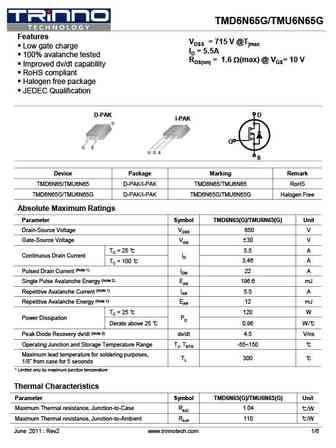
tmd6n65g tmu6n65g.pdf
TMD6N65G/TMU6N65G Features VDSS = 715 V @Tjmax Low gate charge ID = 5.5A 100% avalanche tested RDS(on) = 1.6 W(max) @ VGS= 10 V Improved dv/dt capability RoHS compliant Halogen free package JEDEC Qualification D-PAK D I-PAK G S Device Package Marking Remark TMD6N65/TMU6N65 D-PAK/I-PAK TMD6N65/TMU6N65 RoHS TMD6N65G/TMU6N65G D-PAK/I-PAK TM
tmp6n65 tmpf6n65.pdf
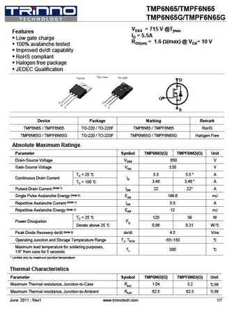
TMP6N65/TMPF6N65 TMP6N65G/TMPF6N65G VDSS = 715 V @Tjmax Features ID = 5.5A Low gate charge RDS(on) = 1.6 W(max) @ VGS= 10 V 100% avalanche tested Improved dv/dt capability RoHS compliant Halogen free package JEDEC Qualification D G S Device Package Marking Remark TMP6N65 / TMPF6N65 TO-220 / TO-220F TMP6N65 / TMPF6N65 RoHS TMP6N65G / TMPF
tsf16n65mr.pdf
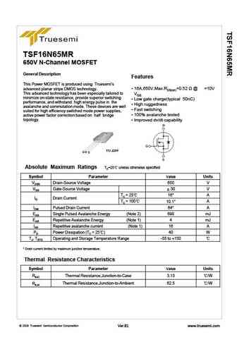
TSF16N65MR 650V N-Channel MOSFET General Description Features This Power MOSFET is produced using Truesemi s 16A,650V,Max.RDS(on)=0.52 @ =10V advanced planar stripe DMOS technology. This advanced technology has been especially tailored to VGS minimize on-state resistance, provide superior switching Low gate charge(typical 50nC) performance, and withstand high e
qm06n65f.pdf
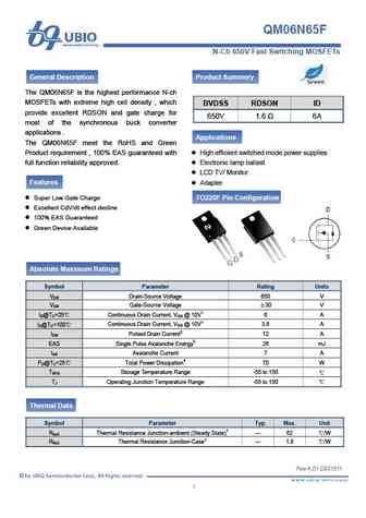
QM06N65F 1 2011-04-25 - 1 - N-Ch 650V Fast Switching MOSFETs General Description Product Summery The QM06N65F is the highest performance N-ch MOSFETs with extreme high cell density , which BVDSS RDSON ID provide excellent RDSON and gate charge for 650V 1.6 6A most of the synchronous buck converter applications . Applications The QM06N65F meet the RoHS and
wml36n65f2 wmk36n65f2 wmn36n65f2 wmm36n65f2 wmj36n65f2.pdf

WML36N65F2, WM F2 MK36N65F WMN3 N65F2, WM F2 36N65F2, WMM36N MJ36N65F 650V 0.087 S 0 Super Junction Power MOSFET Descrip ption WMOSTM F2 is Wa 2nd generation super ayon s junction MOSFET fam with fa body di F2 M mily ast iode. S series pro all benefits of a fast switching ovide b f s S D D G G G S D G SJ-MOSFE while of an extremely fa body ET ffering
wml26n65c4 wmo26n65c4 wmk26n65c4 wmn26n65c4 wmm26n65c4 wmj26n65c4.pdf

WML26N65C4, WMO26N6 WM C4 W 65C4, MK26N65C WMN2 MJ26N65C 26N65C4, WMM26N65C4, WM C4 650V 0.16 S T V Super Junction Power MOSFET Descrip ption WMOSTM C4 is Wa 4th generation super ayon s n junction MOSFET fa that is utilizing charge M amily S balance te or extremely esistance echnology fo y low on-re S D D G G G S D G and low ga charge performanc WMOSTM
wml16n65sr wmk16n65sr wmm16n65sr wmn16n65sr wmp16n65sr wmo16n65sr.pdf
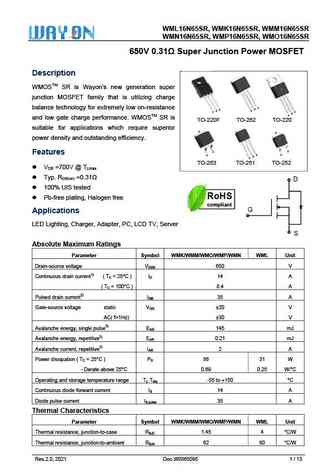
WML16N65SR, W 65SR, WM SR WMK16N6 MM16N65S WMN16N65SR, WMP16N6 MO16N65S 65SR, WM SR 650V 0.31 S unction P MOSFET 0 Super Ju Power M T Descrip ption WMOSTM SR is Wa new generation super ayon s w junction MOSFET fa that is utilizing charge M amily S balance te or extremely esistance echnology fo y low on-re D S D G G G S D G T and low ga charge perfo
wml26n65f2 wmo26n65f2 wmk26n65f2 wmn26n65f2 wmm26n65f2 wmj26n65f2.pdf
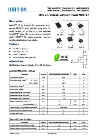
WML2 N65F2, WM F2 26N65F2, WMO26N MK26N65F WMN2 N65F2, WM F2 26N65F2, WMM26N MJ26N65F 650V 0.17 S T V Super Junction Power MOSFET Descrip ption WMOSTM F2 is Wa 2nd generation super ayon s junction MOSFET fam with fa body di F2 M mily ast iode. S series pro all benefits of a fast switching ovide b f s S D D G G G S D G SJ-MOSFE while of an extremely fa
wml26n65sr wmk26n65sr wmn26n65sr wmm26n65sr wmj26n65sr.pdf
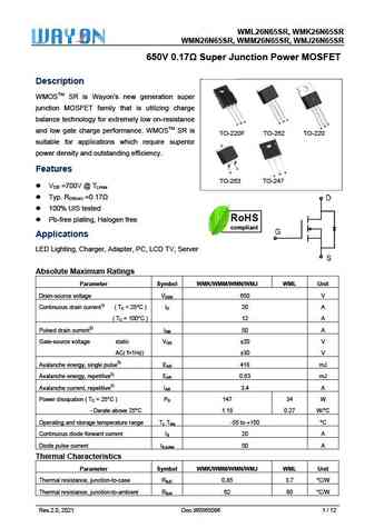
WML26N6 MK26N65S 65SR, WM SR WMN2 MJ26N65S 26N65SR, WMM26N65SR, WM SR 650V 0.17 S unction Power M T Super Ju MOSFET Descrip ption WMOSTM SR is Wa new generation super ayon s w junction MOSFET fa that is utilizing charge M amily S balance te or extremely esistance echnology fo y low on-re S D D G G G S D G T and low ga charge performanc WMOSTM SR is
wml26n65c4 wmk26n65c4 wmn26n65c4 wmm26n65c4 wmo26n65c4 wmj26n65c4.pdf

WML26N65C4, WMO26N6 WM C4 W 65C4, MK26N65C WMN2 MJ26N65C 26N65C4, WMM26N65C4, WM C4 650V 0.16 S T V Super Junction Power MOSFET Descrip ption WMOSTM C4 is Wa 4th generation super ayon s n junction MOSFET fa that is utilizing charge M amily S balance te or extremely esistance echnology fo y low on-re S D D G G G S D G and low ga charge performanc WMOSTM
wml36n65c4 wmk36n65c4 wmn36n65c4 wmm36n65c4 wmj36n65c4.pdf
WML36N6 WM C4 65C4, MK36N65C WMN3 MJ36N65C 36N65C4, WMM36N65C4, WM C4 650V 0.08 S T V Super Junction Power MOSFET Descrip ption WMOSTM C4 is Wa 4th generation super ayon s n junction MOSFET fa that is utilizing charge M amily S balance te or extremely esistance echnology fo y low on-re S D D G G G S D G and low ga charge performanc WMOSTM C4 is ate c
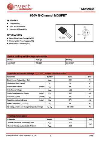
cs16n65fa9h.pdf
Silicon N-Channel Power MOSFET R CS16N65F A9H VDSS 650 V General Description ID 16 A CS16N65F A9H, the silicon N-channel Enhanced PD(TC=25 ) 70 W VDMOSFETs, is obtained by the self-aligned planar Technology RDS(ON)Typ 0.49 which reduce the conduction loss, improve switching performance and enhance the avalanche energy. The transistor can be used in various po
cs6n65f cs6n65p cs6n65u cs6n65d.pdf
nvert Suzhou Convert Semiconductor Co ., Ltd. CS6N65F,CS6N65P,CS6N65U,CS6N65D 650V N-Channel MOSFET FEATURES Fast switching 100% avalanche tested Improved dv/dt capability APPLICATIONS Switch Mode Power Supply (SMPS) Uninterruptible Power Supply (UPS) Power Factor Correction (PFC) Device Marking and Package Information Device Package Marking CS6N65F TO-220F
cs16n65f cs16n65p cs16n65w.pdf
nvert CS16N65F,CS16N65P,CS16N65W Suzhou Convert Semiconductor Co ., Ltd. 650V N-Channel MOSFET FEATURES Fast switching 100% avalanche tested Improved dv/dt capability APPLICATIONS Switch Mode Power Supply (SMPS) Uninterruptible Power Supply (UPS) Power Factor Correction (PFC) Device Marking and Package Information Device Package Marking CS16N65F TO-220F CS1
cs16n65f.pdf
nvert Suzhou Convert Semiconductor Co ., Ltd. CS16N65F 650V N-Channel MOSFET FEATURES Fast switching 100% avalanche tested Improved dv/dt capability APPLICATIONS Switch Mode Power Supply (SMPS) Uninterruptible Power Supply (UPS) Power Factor Correction (PFC) Device Marking and Package Information Device Package Marking CS16N65F TO-220F CS16N65F Absolute Max
smf16n65.pdf
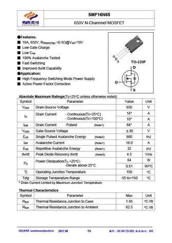
SMF16N65 650V N-Channnel MOSFET Features 16A, 650V, R =0.5 @V =10V DS(on)(Typ) GS Low Gate Charge Low C rss 100% Avalanche Tested Fast Switching Improved dv/dt Capability Application High Frequency Switching Mode Power Supply Active Power Factor Correction Absolute Maximum Ratings(Tc=25 C unless otherwise noted) Symbol Parameter Value
jmpf16n65bj.pdf
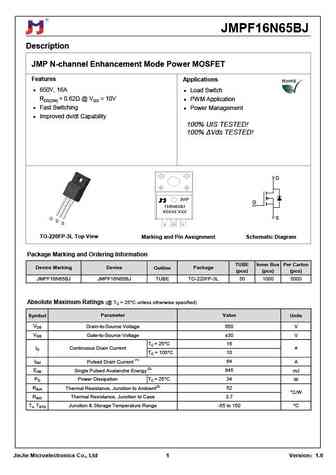
JMPF16N65BJ Description JMP N-channel Enhancement Mode Power MOSFET Features Applications 650V, 16A Load Switch RDS(ON)
jjt6n65ss.pdf
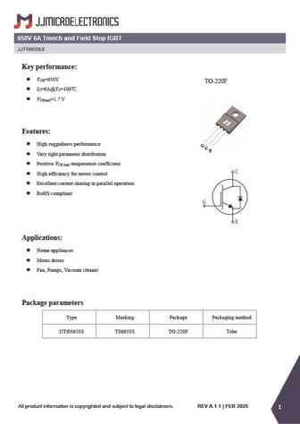
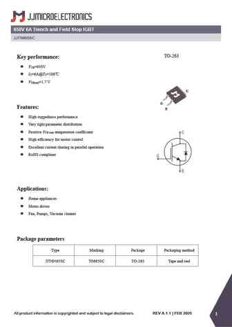
650V 6A Trench and Field Stop IGBT JJT6N65SS Key performance V =650V CE TO-220F I =6A@T =100 C C V =1.7 V CE(sat) Features High ruggedness performance G C E Very tight parameter distribution Positive V temperature coefficient CE (sat) High efficiency for motor control Excellent current sharing in parallel operation RoHS compliant App
jjt6n65st.pdf
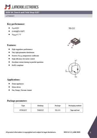
650V 6A Trench and Field Stop IGBT JJT6N65ST Key performance V =650V CE TO-252 I =6A@T =100 C C V =1.7 V CE(sat) C Features G E High ruggedness performance Very tight parameter distribution Positive V temperature coefficient CE (sat) High efficiency for motor control Excellent current sharing in parallel operation RoHS compliant Appli
jmpc16n65bj.pdf
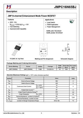
JMPC16N65BJ Description JMP N-channel Enhancement Mode Power MOSFET Features Applications 650V, 16A Load Switch RDS(ON)
jjt6n65std.pdf
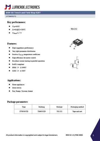
650V 6A Trench and Field Stop IGBT JJT6N65STD Key performance V =650V CE TO-252 I =6A@T =100 C C V =1.7 V CE(sat) C Features G High ruggedness performance E Very tight parameter distribution Positive V temperature coefficient CE (sat) High efficiency for motor control Excellent current sharing in parallel operation RoHS compliant
jjt6n65sc.pdf
650V 6A Trench and Field Stop IGBT JJT6N65SC TO-263 Key performance V =650V CE I =6A@T =100 C C V =1.7 V CE(sat) C G Features E High ruggedness performance Very tight parameter distribution Positive V temperature coefficient CE (sat) High efficiency for motor control Excellent current sharing in parallel operation RoHS compliant Appl
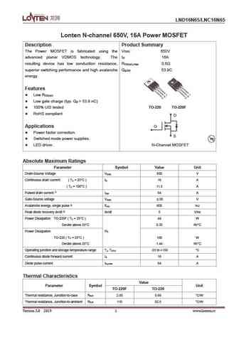
lnd16n65 lnc16n65.pdf
LND16N65/LNC16N65 Lonten N-channel 650V, 16A Power MOSFET Description Product Summary The Power MOSFET is fabricated using the V 650V DSS advanced planer VDMOS technology. The I 16A D resulting device has low conduction resistance, R 0.6 DS(on),max superior switching performance and high avalanche Q 53.9C g,typ energy. Features Low R DS(on) Low gate charge (typ. Q = 53.
agm16n65f.pdf
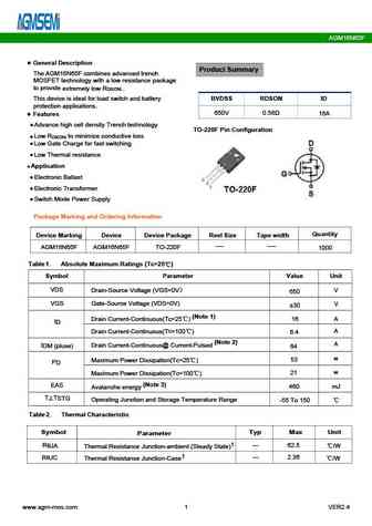
AGM16N65F General Description Product Summary The AGM16N65F combines advanced trench MOSFET technology with a low resistance package to provide extremely low R . DS(ON) This device is ideal switch and battery BVDSS RDSON ID for load protection applications. 650V 0.58 16A Features Advance high cell density Trench technology TO-220F Pin Configuration Low R to m
spc16n65g.pdf
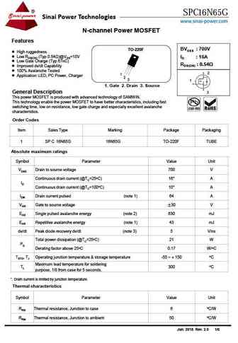
SPC16N65G Sinai Power Technologies www.sinai-power.com N-channel Power MOSFET Features TO-220F BVDSS 700V High ruggedness Low RDS(ON) (Typ 0.54 )@VGS=10V ID 16A Low Gate Charge (Typ 67nC) RDS(ON) 0.54 Improved dv/dt Capability 100% Avalanche Tested 2 1 Application LED, PC Power, Charger 2 3 1 1. Gate 2. Drain 3. Source
smirf16n65.pdf
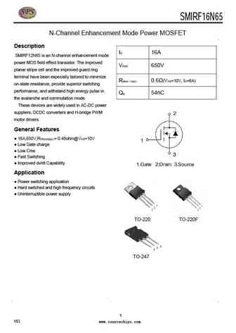
SMIRF16N65 30V /36A Single N Power MOSFET N-Channel Enhancement Mode Power MOSFET Description ID 16A SMIRF12N65 is an N-channel enhancement mode power MOS field effect transistor. The improved VDSS 650V planar stripe cell and the improved guard ring terminal have been especially tailored to minimize Rdson max 0.6 (VGS=10V, ID=8A) on-state resistance, provide superior
hm16n65f.pdf
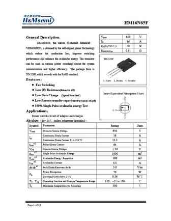
HM16N65F VDSS 650 V General Description ID 16 A HM16N65F, the silicon N-channel Enhanced PD(TC=25 ) 70 W VDMOSFETs, is obtained by the self-aligned planar Technology RDS(ON)Typ 0.51 which reduce the conduction loss, improve switching performance and enhance the avalanche energy. The transistor can be used in various power switching circuit for system miniaturizati
mpbd6n65esf mpbc6n65esf.pdf
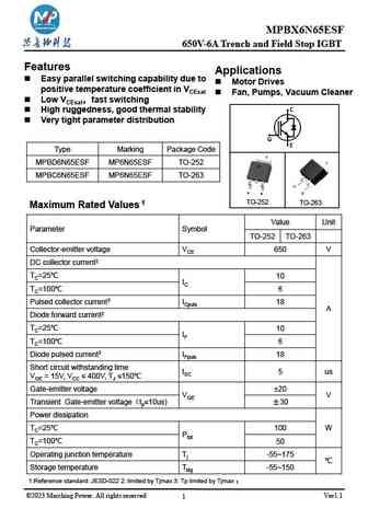
MPBX6N65ESF 650V-6A Trench and Field Stop IGBT Features Applications Easy parallel switching capability due to Motor Drives positive temperature coefficient in VCEsat Fan, Pumps, Vacuum Cleaner Low VCEsat fast switching High ruggedness, good thermal stability Very tight parameter distribution Type Marking Package Code C C MPBD6N65ESF MP6N65ESF TO-252 MPB
mdi6n65bth.pdf
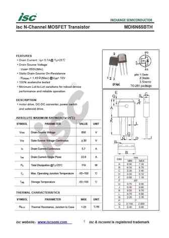
isc N-Channel MOSFET Transistor MDI6N65BTH FEATURES Drain Current I = 5.7A@ T =25 D C Drain Source Voltage V = 650V(Min) DSS Static Drain-Source On-Resistance R = 1.45 (Max) @V = 10V DS(on) GS 100% avalanche tested Minimum Lot-to-Lot variations for robust device performance and reliable operation DESCRIPTION motor drive, DC-DC converter, power switch and sol
ixfh46n65x2.pdf
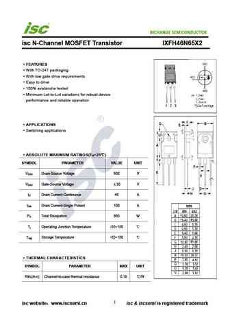
INCHANGE Semiconductor isc N-Channel MOSFET Transistor IXFH46N65X2 FEATURES With TO-247 packaging With low gate drive requirements Easy to drive 100% avalanche tested Minimum Lot-to-Lot variations for robust device performance and reliable operation APPLICATIONS Switching applications ABSOLUTE MAXIMUM RATINGS(T =25 ) a SYMBOL PARAMETER VALUE UNIT V Drain-Source
16n65mf.pdf
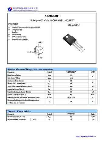
16N65MF 16 Amps,650 Volts N-CHANNEL MOSFET FEATURE TO-220MF 16A,650V,R =0.45 @V =10V/8A DS(ON)MAX GS Low gate charge Low C iss Fast switching 100% avalanche tested Improved dv/dt capability Absolute Maximum Ratings(T =25 ,unless otherwise noted) C Parameter Symbol UNIT 16N65MF Drain-Source Voltage V 650 DSS V Gate-Source Voltage V 30 GSS Continu
Otros transistores... 3N65 , 3N65Z , 3N65K , 4N65 , 4N65Z , 4N65K , 5N65 , 5N65K , IRFZ48N , 5N60 , 6N60 , 6N60Z , 7N60A , 7N60 , 7N60Z , 7N60K , 8N60 .
🌐 : EN ES РУ

Liste
Recientemente añadidas las descripciónes de los transistores:
MOSFET: ASA60R150E | ASA60R090EFDA | ASA60R090EFD | ASA50R130E | ADW120N080G2 | ADQ120N080G2 | ADG120N080G2 | AS6004 | 2N7002EY | AS2310A | 2N7002KM | 2N7002KH | AON5802 | AOSS62934 | AOSN21319C | AONS66966
Popular searches
2sc1344 | cs840f | 2n3053 equivalent | 2n3569 | 2sd667 | 2sc1111 | bc239 transistor equivalent | 3sk41