20N60 Datasheet. Equivalente. Reemplazo. Hoja de especificaciones. Principales características
Número de Parte: 20N60
Tipo de FET: MOSFET
Polaridad de transistor: N
ESPECIFICACIONES MÁXIMAS
Pdⓘ - Máxima disipación de potencia: 416 W
|Vds|ⓘ - Voltaje máximo drenador-fuente: 600 V
|Vgs|ⓘ - Voltaje máximo fuente-puerta: 30 V
|Id|ⓘ - Corriente continua de drenaje: 20 A
Tjⓘ - Temperatura máxima de unión: 150 °C
CARACTERÍSTICAS ELÉCTRICAS
trⓘ - Tiempo de subida: 130 nS
Cossⓘ - Capacitancia de salida: 330 pF
RDSonⓘ - Resistencia estado encendido drenaje a fuente: 0.32 Ohm
Encapsulados: TO-3P TO-247 TO-230
Búsqueda de reemplazo de 20N60 MOSFET
- Selecciónⓘ de transistores por parámetros
20N60 datasheet
20n60.pdf
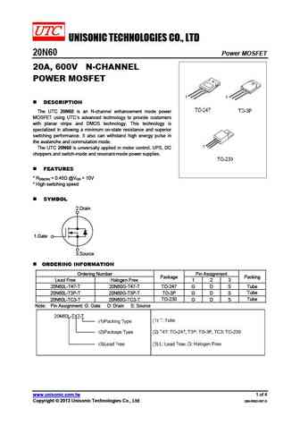
UNISONIC TECHNOLOGIES CO., LTD 20N60 Power MOSFET 20A, 600V N-CHANNEL POWER MOSFET DESCRIPTION The UTC 20N60 is an N-channel enhancement mode power MOSFET using UTC s advanced technology to provide customers with planar stripe and DMOS technology. This technology is specialized in allowing a minimum on-state resistance and superior switching performance. It also can withst
hgtg20n60b3d.pdf
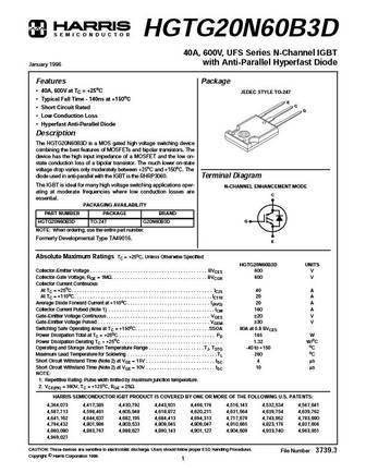
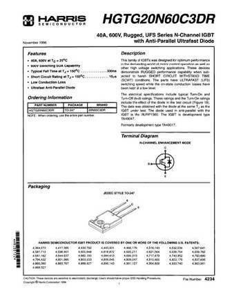
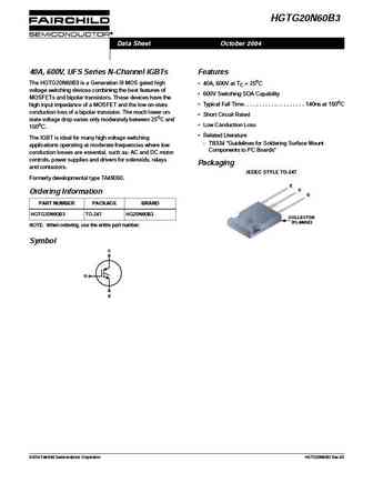
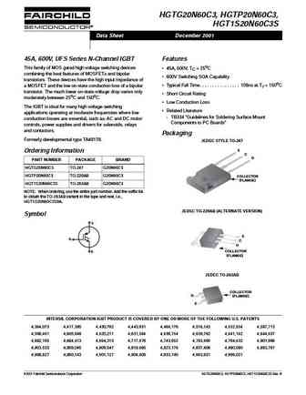
S E M I C O N D U C T O R HGTG20N60B3D 40A, 600V, UFS Series N-Channel IGBT with Anti-Parallel Hyperfast Diode January 1996 Features Package 40A, 600V at TC = +25oC JEDEC STYLE TO-247 Typical Fall Time - 140ns at +150oC E C Short Circuit Rated G Low Conduction Loss Hyperfast Anti-Parallel Diode Description The HGTG20N60B3D is a MOS gated high voltage switching
hgt1s20n60b3s hgtp20n60b3 hgtg20n60b3.pdf
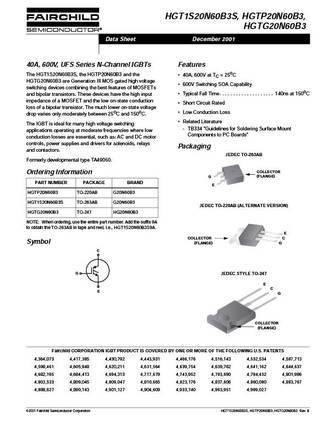
HGT1S20N60B3S, HGTP20N60B3, HGTG20N60B3 Data Sheet December 2001 40A, 600V, UFS Series N-Channel IGBTs Features The HGT1S20N60B3S, the HGTP20N60B3 and the 40A, 600V at TC = 25oC HGTG20N60B3 are Generation III MOS gated high voltage 600V Switching SOA Capability switching devices combining the best features of MOSFETs Typical Fall Time. . . . . . . . . . . . . . . . . . .
hgtp20n60b3 hgtg20n60b3.pdf
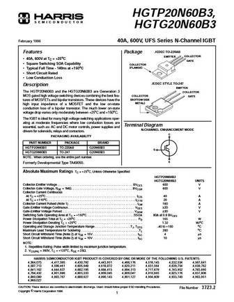
HGTP20N60B3, S E M I C O N D U C T O R HGTG20N60B3 February 1996 40A, 600V, UFS Series N-Channel IGBT JEDEC TO-220AB Features Package EMITTER COLLECTOR 40A, 600V at TC = +25oC GATE Square Switching SOA Capability COLLECTOR (FLANGE) Typical Fall Time - 140ns at +150oC Short Circuit Rated Low Conduction Loss JEDEC STYLE TO-247 Description EMITTER The HGTP20N6
fqpf20n60 fqp20n60.pdf
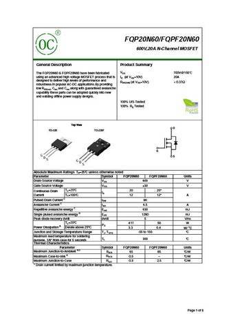
FQP20N60/FQPF20N60 600V,20A N-Channel MOSFET General Description Product Summary VDS 700V@150 The FQP20N60 & FQPF20N60 have been fabricated using an advanced high voltage MOSFET process that is ID (at VGS=10V) 20A designed to deliver high levels of performance and RDS(ON) (at VGS=10V)
hgtp20n60c3r hgtg20n60c3r hgt1s20n60c3r hgt1s20n60c3rs.pdf

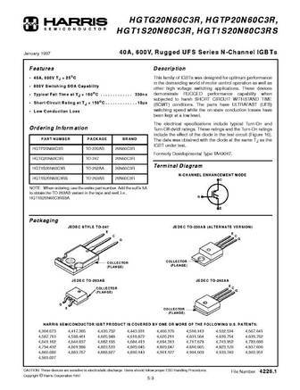
HGTG20N60C3R, HGTP20N60C3R, S E M I C O N D U C T O R HGT1S20N60C3R, HGT1S20N60C3RS 40A, 600V, Rugged UFS Series N-Channel IGBTs January 1997 Features Description 40A, 600V TJ = 25oC This family of IGBTs was designed for optimum performance in the demanding world of motor control operation as well as 600V Switching SOA Capability other high voltage switching applications. These
mgw20n60d.pdf

MOTOROLA Order this document SEMICONDUCTOR TECHNICAL DATA by MGW20N60D/D Designer's Data Sheet MGW20N60D Insulated Gate Bipolar Transistor Motorola Preferred Device with Anti-Parallel Diode N Channel Enhancement Mode Silicon Gate IGBT & DIODE IN TO 247 20 A @ 90 C This Insulated Gate Bipolar Transistor (IGBT) is co packaged 32 A @ 25 C with a soft recovery ultra fas
mgp20n60urev0.pdf
MOTOROLA Order this document SEMICONDUCTOR TECHNICAL DATA by MGP20N60U/D Product Preview MGP20N60U Insulated Gate Bipolar Transistor N Channel Enhancement Mode Silicon Gate This Insulated Gate Bipolar Transistor (IGBT) uses an advanced IGBT IN TO 220 termination scheme to provide an enhanced and reliable high 20 A @ 90 C voltage blocking capability. It also provides fast sw
mgp20n60u.pdf
MOTOROLA Order this document SEMICONDUCTOR TECHNICAL DATA by MGP20N60U/D Designer's Data Sheet MGP20N60U Insulated Gate Bipolar Transistor N Channel Enhancement Mode Silicon Gate This Insulated Gate Bipolar Transistor (IGBT) uses an advanced IGBT IN TO 220 termination scheme to provide an enhanced and reliable high 20 A @ 90 C voltage blocking capability. It also provide
mgw20n60.pdf

MOTOROLA Order this document SEMICONDUCTOR TECHNICAL DATA by MGW20N60D/D Designer's Data Sheet MGW20N60D Insulated Gate Bipolar Transistor Motorola Preferred Device with Anti-Parallel Diode N Channel Enhancement Mode Silicon Gate IGBT & DIODE IN TO 247 20 A @ 90 C This Insulated Gate Bipolar Transistor (IGBT) is co packaged 32 A @ 25 C with a soft recovery ultra fas
tk20n60w.pdf
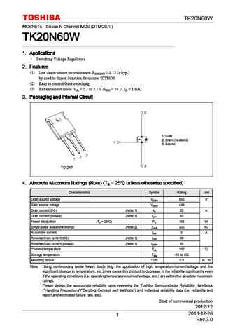
TK20N60W MOSFETs Silicon N-Channel MOS (DTMOS ) TK20N60W TK20N60W TK20N60W TK20N60W 1. Applications 1. Applications 1. Applications 1. Applications Switching Voltage Regulators 2. Features 2. Features 2. Features 2. Features (1) Low drain-source on-resistance RDS(ON) = 0.13 (typ.) by used to Super Junction Structure DTMOS (2) Easy to control Gate switching (3) En
tk20n60w5.pdf
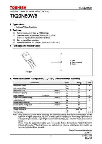
TK20N60W5 MOSFETs Silicon N-Channel MOS (DTMOS ) TK20N60W5 TK20N60W5 TK20N60W5 TK20N60W5 1. Applications 1. Applications 1. Applications 1. Applications Switching Voltage Regulators 2. Features 2. Features 2. Features 2. Features (1) Fast reverse recovery time trr = 110 ns (typ.) (2) Low drain-source on-resistance RDS(ON) = 0.15 (typ.) by used to Super Junction Str
fcb20n60f f085.pdf
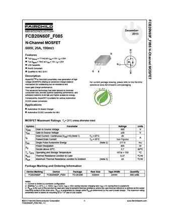
December 2013 FCB20N60F_F085 N-Channel MOSFET 600V, 20A, 190m D D Features Typ rDS(on) = 171m at VGS = 10V, ID = 20A Typ Qg(tot) = 78nC at VGS = 10V, ID = 20A G UIS Capability RoHS Compliant G Qualified to AEC Q101 S S Description SuperFETTM is Fairchild s proprietary new generation of high voltage MOSFETs utilizing an advanced charge balance For current pack
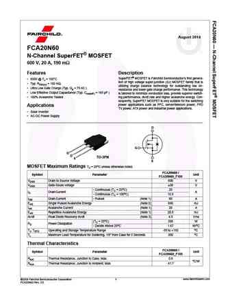
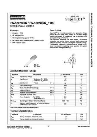
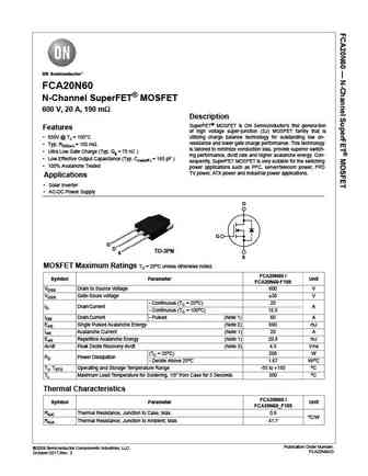
fch20n60 fca20n60 fca20n60 f109.pdf
December 2008 TM SuperFET FCH20N60 / FCA20N60 / FCA20N60_F109 600V N-Channel MOSFET Features Description 650V @TJ = 150 C SuperFETTM is, Fairchild s proprietary, new generation of high voltage MOSFET family that is utilizing an advanced charge Typ. Rds(on)=0.15 balance mechanism for outstanding low on-resistance and Ultra low gate charge (typ. Qg=55nC) lower gate cha
fgh20n60sfd.pdf
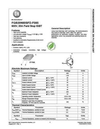
September 2008 FGH20N60SFD tm 600V, 20A Field Stop IGBT Features General Description High current capability Using Novel Field Stop IGBT Technology, Fairchild s new series of Field Stop IGBTs offer the optimum performance for Induction Low saturation voltage VCE(sat) =2.2V @ IC = 20A Heating, UPS, SMPS and PFC applications where low conduc- High input impedance tion an
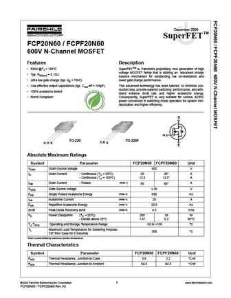
fcp20n60 fcpf20n60.pdf
August 2014 FCP20N60 / FCPF20N60 N-Channel SuperFET MOSFET 600 V, 20 A, 190 m Features Description SuperFET MOSFET is Fairchild Semiconductor s first genera- 650V @ TJ = 150 C tion of high voltage super-junction (SJ) MOSFET family that is Typ. RDS(on) = 150 m utilizing charge balance technology for outstanding low on- Ultra Low Gate Charge (Typ. Qg = 75 nC ) r
fca20n60f fca20n60fs.pdf
December 2008 TM SuperFET FCA20N60F 600V N-CHANNEL FRFET Features Description 650V @TJ = 150 C SuperFETTM is, Fairchild s proprietary, new generation of high voltage MOSFET family that is utilizing an advanced charge Typ. Rds(on)=0.15 balance mechanism for outstanding low on-resistance and Fast Recovery Type ( trr = 160ns ) lower gate charge performance. This a
fcp20n60fs fcp20n60 fcpf20n60.pdf
December 2008 TM SuperFET FCP20N60 / FCPF20N60 600V N-Channel MOSFET Features Description 650V @TJ = 150 C SuperFETTM is, Fairchild s proprietary, new generation of high voltage MOSFET family that is utilizing an advanced charge Typ. RDS(on) = 0.15 balance mechanism for outstanding low on-resistance and Ultra low gate charge (typ. Qg = 75nC) lower gate charge perfo
fca20n60 fca20n60 f109.pdf
August 2014 FCA20N60 N-Channel SuperFET MOSFET 600 V, 20 A, 190 m Features Description SuperFET MOSFET is Fairchild Semiconductor s first genera- 650V @ TJ = 150 C tion of high voltage super-junction (SJ) MOSFET family that is Typ. RDS(on) = 150 m utilizing charge balance technology for outstanding low on- Ultra Low Gate Charge (Typ. Qg = 75 nC ) resistance an
fcd620n60zf.pdf
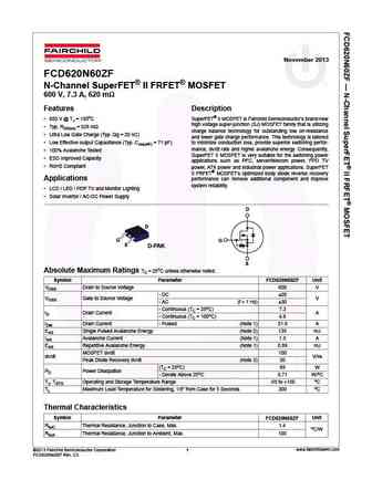
November 2013 FCD620N60ZF N-Channel SuperFET II FRFET MOSFET 600 V, 7.3 A, 620 m Features Description 650 V @ TJ = 150oC SuperFET II MOSFET is Fairchild Semiconductor s brand-new high voltage super-junction (SJ) MOSFET family that is utilizing Typ. RDS(on) = 528 m charge balance technology for outstanding low on-resistance Ultra Low Gate Charge (Typ. Qg = 20 nC)
hgtg20n60b3d.pdf
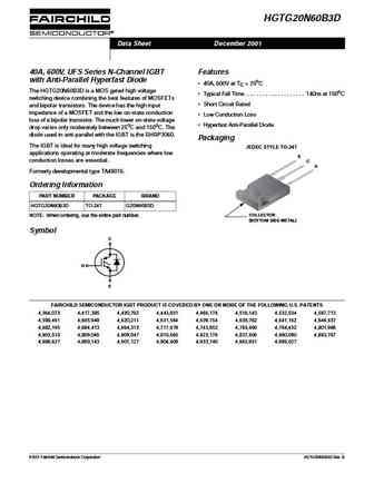
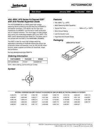
HGTG20N60B3D Data Sheet December 2001 40A, 600V, UFS Series N-Channel IGBT Features with Anti-Parallel Hyperfast Diode 40A, 600V at TC = 25oC The HGTG20N60B3D is a MOS gated high voltage Typical Fall Time. . . . . . . . . . . . . . . . . . . . 140ns at 150oC switching device combining the best features of MOSFETs Short Circuit Rated and bipolar transistors. The device has
fcb20n60 f085.pdf
November 2013 FCB20N60_F085 N-Channel MOSFET 600V, 20A, 198m D D Features Typ rDS(on) = 173m at VGS = 10V, ID = 20A Typ Qg(tot) = 72nC at VGS = 10V, ID = 20A G UIS Capability RoHS Compliant G Qualified to AEC Q101 S S Description SuperFETTM is Fairchild s proprietary new generation of high voltage MOSFETs utilizing an advanced charge balance For current packa
fgh20n60ufd.pdf
April 2011 FGH20N60UFD 600V, 20A Field Stop IGBT Features General Description High current capability Using Novel Field Stop IGBT Technology, Fairchild s new series of Field Stop IGBTs offer the optimum performance for Induc- Low saturation voltage VCE(sat) =1.8V @ IC = 20A tion Heating, UPS, SMPS and PFC applications where low con- High input impedance duction and switc
fgb20n60sf.pdf
March 2015 FGB20N60SF 600 V, 20 A Field Stop IGBT Features General Description High Current Capability Using novel field stop IGBT technology, Fairchild s field stop IGBTs offer the optimum performance for solar inverter, UPS, Low Saturation Voltage VCE(sat) =2.2 V @ IC = 20 A welder and PFC applications where low conduction and switch- High Input Impedance ing losses
hgtg20n60a4d.pdf
HGTG20N60A4D Data Sheet February 2009 600V, SMPS Series N-Channel IGBT with Features Anti-Parallel Hyperfast Diode >100kHz Operation At 390V, 20A The HGTG20N60A4D is a MOS gated high voltage switching 200kHz Operation At 390V, 12A device combining the best features of MOSFETs and bipolar 600V Switching SOA Capability transistors. This device has the high input impedance o
fgp20n60ufd.pdf
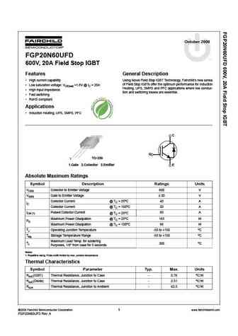
October 2008 FGP20N60UFD tm 600V, 20A Field Stop IGBT Features General Description High current capability Using Novel Field Stop IGBT Technology, Fairchild s new series of Field Stop IGBTs offer the optimum performance for Induction Low saturation voltage VCE(sat) =1.8V @ IC = 20A Heating, UPS, SMPS and PFC applications where low conduc- High input impedance tion and s
fca20n60s fca20n60s f109.pdf
August 2007 TM SuperFET FCA20N60S / FCA20N60S_F109 600V N-Channel MOSFET Features Description 650V @TJ = 150 C SuperFETTM is, Farichild s proprietary, new generation of high voltage MOSFET family that is utilizing an advanced charge Typ. Rds(on)=0.22 balance mechanism for outstanding low on-resistance and Ultra low gate charge (typ. Qg=55nC) lower gate charge perform
fcb20n60ftm.pdf

December 2008 TM SuperFET FCB20N60F 600V N-CHANNEL FRFET Features Description 650V @ TJ = 150 C SuperFETTM is,Fairchild' s proprietary, new generation of high voltage MOSFET family that is utilizing an advanced charge Typ. Rds(on)=0.15 balance mechanism for outstanding low on-resistance and Fast Recovery Type ( trr = 160ns ) lower gate charge performance. This a
sgh20n60rufd.pdf
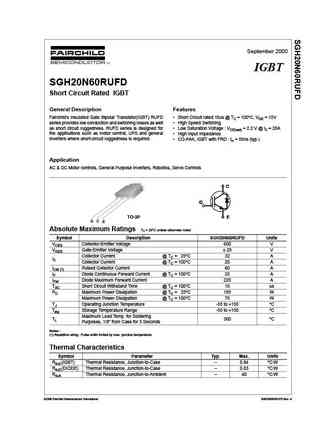
September 2000 IGBT SGH20N60RUFD Short Circuit Rated IGBT General Description Features Fairchild's Insulated Gate Bipolar Transistor(IGBT) RUFD Short Circuit rated 10us @ TC = 100 C, VGE = 15V series provides low conduction and switching losses as well High Speed Switching as short circuit ruggedness. RUFD series is designed for Low Saturation Voltage VCE(sat) = 2.2 V @
hgtg20n60a4 hgtp20n60a4.pdf
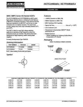
HGTG20N60A4, HGTP20N60A4 Data Sheet December 2001 600V, SMPS Series N-Channel IGBTs Features The HGTG20N60A4 and HGTP20N60A4 are MOS gated >100kHz Operation at 390V, 20A high voltage switching devices combining the best features 200kHz Operation at 390V, 12A of MOSFETs and bipolar transistors. These devices have the 600V Switching SOA Capability high input impedance of a
hgtg20n60b3.pdf
HGTG20N60B3 Data Sheet October 2004 40A, 600V, UFS Series N-Channel IGBTs Features The HGTG20N60B3 is a Generation III MOS gated high 40A, 600V at TC = 25oC voltage switching devices combining the best features of 600V Switching SOA Capability MOSFETs and bipolar transistors. These devices have the Typical Fall Time. . . . . . . . . . . . . . . . . . . . 140ns at 150oC h
fgb20n60sfd.pdf
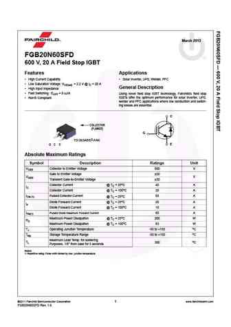
March 2015 FGB20N60SFD 600 V, 20 A Field Stop IGBT Features Applications High Current Capability Solar Inverter, UPS, Welder, PFC Low Saturation Voltage VCE(sat) = 2.2 V @ IC = 20 A General Description High Input Impedance Fast Switching EOFF = 8 uJ/A Using novel field stop IGBT technology, Fairchild s field stop IGBTs offer the optimum performance for solar i
fcb20n60tm.pdf

December 2008 TM SuperFET FCB20N60 600V N-Channel MOSFET Features Description 650V @TJ = 150 C SuperFETTM is, Fairchild s proprietary, new generation of high voltage MOSFET family that is utilizing an advanced charge Typ. RDS(on) = 0.15 balance mechanism for outstanding low on-resistance and Ultra low gate charge (typ. Qg = 75nC) lower gate charge performance.
fcb20n60f.pdf
December 2008 TM SuperFET FCB20N60F 600V N-CHANNEL FRFET Features Description 650V @ TJ = 150 C SuperFETTM is,Fairchild' s proprietary, new generation of high voltage MOSFET family that is utilizing an advanced charge Typ. Rds(on)=0.15 balance mechanism for outstanding low on-resistance and Fast Recovery Type ( trr = 160ns ) lower gate charge performance. This a
fcb20n60.pdf
December 2008 TM SuperFET FCB20N60 600V N-Channel MOSFET Features Description 650V @TJ = 150 C SuperFETTM is, Fairchild s proprietary, new generation of high voltage MOSFET family that is utilizing an advanced charge Typ. RDS(on) = 0.15 balance mechanism for outstanding low on-resistance and Ultra low gate charge (typ. Qg = 75nC) lower gate charge performance.
fch20n60.pdf

December 2008 TM SuperFET FCH20N60 / FCA20N60 / FCA20N60_F109 600V N-Channel MOSFET Features Description 650V @TJ = 150 C SuperFETTM is, Fairchild s proprietary, new generation of high voltage MOSFET family that is utilizing an advanced charge Typ. Rds(on)=0.15 balance mechanism for outstanding low on-resistance and Ultra low gate charge (typ. Qg=55nC) lower gate cha
hgt1s20n60c3s hgtp20n60c3 hgtg20n60c3.pdf
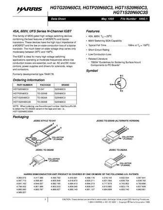
HGTG20N60C3, HGTP20N60C3, HGT1S20N60C3S Data Sheet December 2001 45A, 600V, UFS Series N-Channel IGBT Features This family of MOS gated high voltage switching devices 45A, 600V, TC = 25oC combining the best features of MOSFETs and bipolar 600V Switching SOA Capability transistors. These devices have the high input impedance of Typical Fall Time. . . . . . . . . . . . . .
sgp20n60ruf.pdf
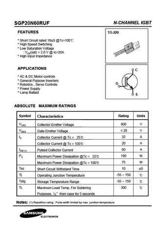
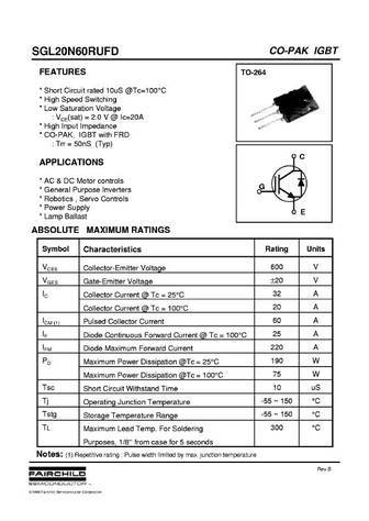
N-CHANNEL IGBT SGP20N60RUF FEATURES TO-220 * Short Circuit rated 10uS @Tc=100 * High Speed Switching * Low Saturation Voltage VCE(sat) = 2.0 V @ Ic=20A * High Input Impedance APPLICATIONS C * AC & DC Motor controls * General Purpose Inverters G * Robotics , Servo Controls * Power Supply * Lamp Ballast E ABSOLUTE MAXIMUM RATINGS Symbol Rating Units Characteristics VCE
sgh20n60rufd.pdf
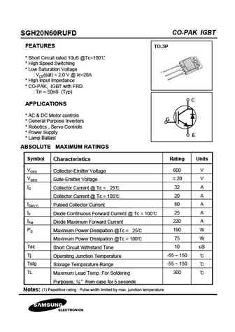
CO-PAK IGBT SGH20N60RUFD FEATURES TO-3P * Short Circuit rated 10uS @Tc=100 * High Speed Switching * Low Saturation Voltage VCE(sat) = 2.0 V @ Ic=20A * High Input Impedance * CO-PAK, IGBT with FRD Trr = 50nS (Typ) C APPLICATIONS * AC & DC Motor controls G * General Purpose Inverters * Robotics , Servo Controls * Power Supply E * Lamp Ballast ABSOLUTE MAXIMUM RATINGS
sgw20n60ruf.pdf
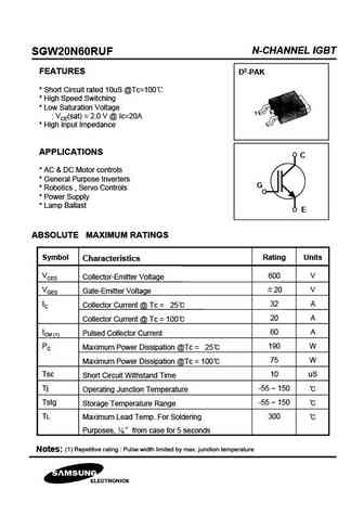
N-CHANNEL IGBT SGW20N60RUF FEATURES D2-PAK * Short Circuit rated 10uS @Tc=100 * High Speed Switching * Low Saturation Voltage VCE(sat) = 2.0 V @ Ic=20A * High Input Impedance APPLICATIONS C * AC & DC Motor controls * General Purpose Inverters G * Robotics , Servo Controls * Power Supply * Lamp Ballast E ABSOLUTE MAXIMUM RATINGS Symbol Rating Units Characteristics VCE
zds020n60.pdf
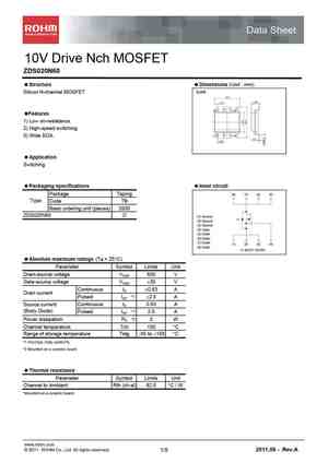
Data Sheet 10V Drive Nch MOSFET ZDS020N60 Structure Dimensions (Unit mm) SOP8 Silicon N-channel MOSFET (8) (5) Features 1) Low on-resistance. 2) High-speed switching. (1) (4) 3) Wide SOA. Application Switching Packaging specifications Inner circuit Package Taping (8) (7) (6) (5) Type Code TB Basic ordering unit (pieces) 2500 ZDS020N60 (1) Source
rdd020n60.pdf
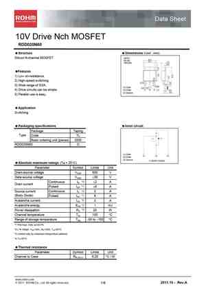
Data Sheet 10V Drive Nch MOSFET RDD020N60 Structure Dimensions (Unit mm) Silicon N-channel MOSFET CPT3 6.5 (SC-63) 5.1 2.3 0.5 Features 1) Low on-resistance. 2) High-speed switching. 0.75 3) Wide range of SOA. 0.65 (1) Gate 0.9 2.3 (1) (2) (3) 4) Drive circuits can be simple. (2) Drain 2.3 0.5 1.0 (3) Source 5) Parallel use is easy. Applicati
sihp120n60e.pdf
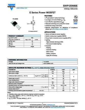
SiHP120N60E www.vishay.com Vishay Siliconix E Series Power MOSFET FEATURES D 4th generation E series technology TO-220AB Low figure-of-merit (FOM) Ron x Qg Low effective capacitance (Co(er)) G Reduced switching and conduction losses Avalanche energy rated (UIS) S Material categorization for definitions of compliance D S please see www.vishay.com/doc?999
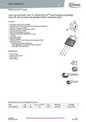
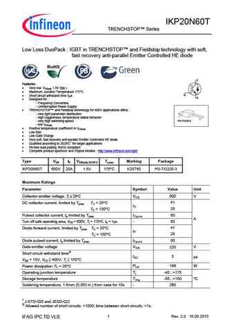
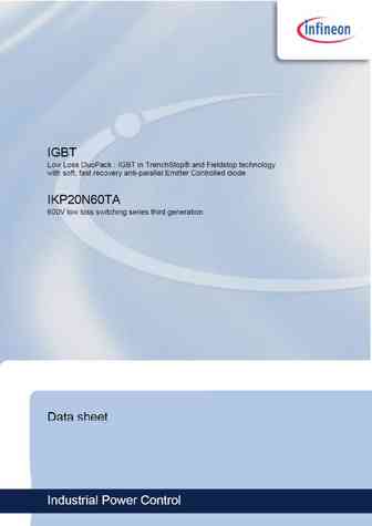
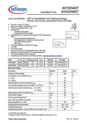
ikp20n60t ikb20n60t ikw20n60t.pdf
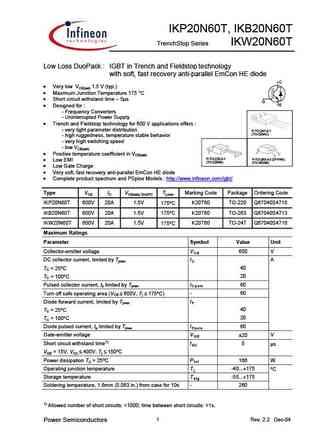
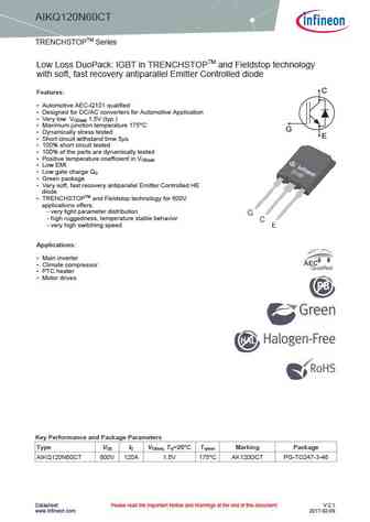
IKP20N60T, IKB20N60T TrenchStop Series IKW20N60T Low Loss DuoPack IGBT in Trench and Fieldstop technology with soft, fast recovery anti-parallel EmCon HE diode C Very low VCE(sat) 1.5 V (typ.) Maximum Junction Temperature 175 C Short circuit withstand time 5 s G E Designed for - Frequency Converters - Uninterrupted Power Supply Trench and F
sgp20n60 sgw20n60.pdf
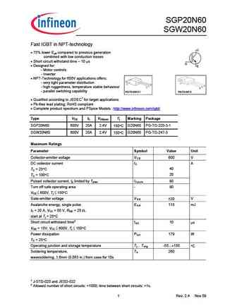
SGP20N60 SGW20N60 Fast IGBT in NPT-technology C 75% lower Eoff compared to previous generation combined with low conduction losses Short circuit withstand time 10 s G Designed for E - Motor controls - Inverter NPT-Technology for 600V applications offers - very tight parameter distribution - high ruggedness, temperature stable behaviour - paral
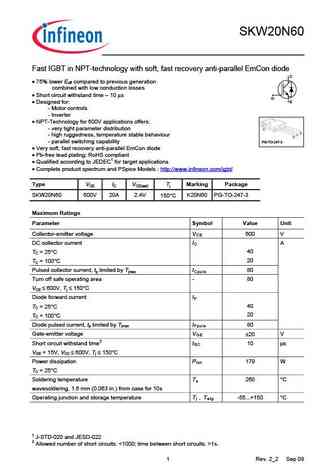
skw20n60.pdf
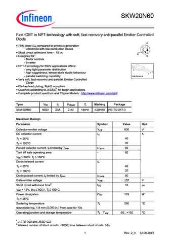
SKW20N60 Fast IGBT in NPT-technology with soft, fast recovery anti-parallel Emitter Controlled Diode C 75% lower Eoff compared to previous generation combined with low conduction losses Short circuit withstand time 10 s G E Designed for - Motor controls - Inverter NPT-Technology for 600V applications offers - very tight parameter distribution - high rugged
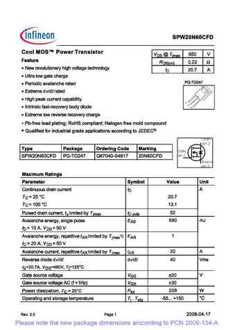
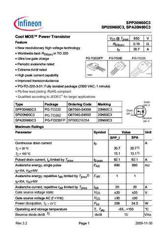
spi20n60cfd.pdf
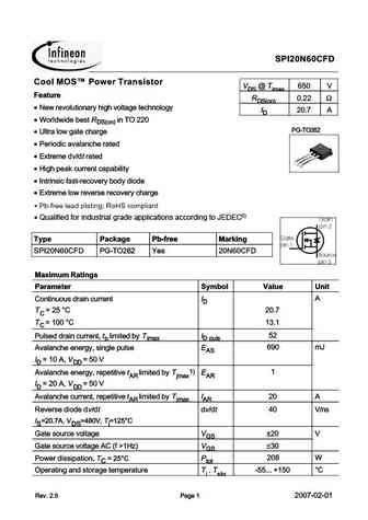
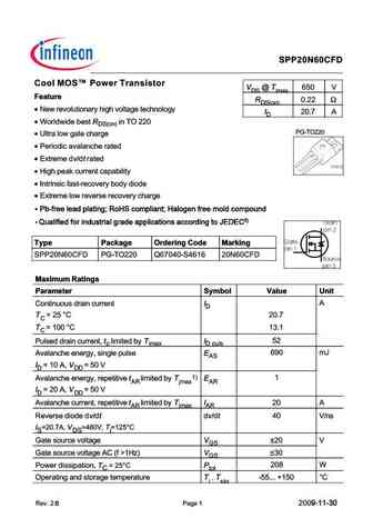
SPI20N60CFD C I MOS P wer Transist r VDS @ Tjmax 650 V Feature RDS(on) 0.22 New revolutionary high voltage technology ID 20.7 A Worldwide best RDS(on) in TO 220 PG-TO262 Ultra low gate charge Periodic avalanche rated Extreme dv/dt rated High peak current capability Intrinsic fast-recovery body diode Extreme low reverse recovery charge Qualifi
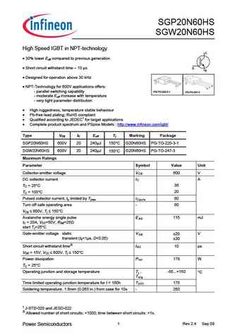
sgp20n60hs sgw20n60hs rev2 5g.pdf

SGP20N60HS SGW20N60HS High Speed IGBT in NPT-technology C 30% lower Eoff compared to previous generation Short circuit withstand time 10 s G E Designed for operation above 30 kHz NPT-Technology for 600V applications offers - parallel switching capability PG-TO-220-3-1 PG-TO-247-3 - moderate Eoff increase with temperature - very tight parameter distri

igw20n60h3 rev1 1g.pdf

IGBT High speed IGBT in Trench and Fieldstop technology IGW20N60H3 600V high speed switching series third generation Datasheet Industrial & Multimarket IGW20N60H3 High speed switching series third generation High speed IGBT in Trench and Fieldstop technology Features C TRENCHSTOPTM technology offering very low V CEsat low EMI Very soft, fast recovery anti-parallel d
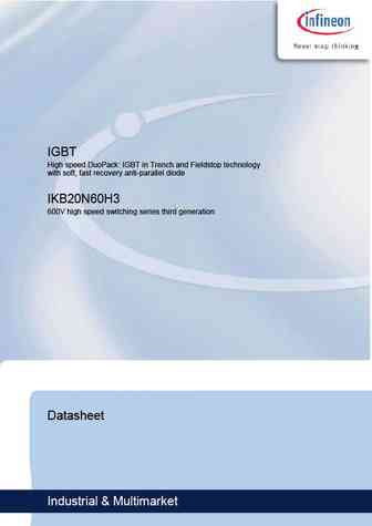
igb20n60h3 rev1 1g.pdf
IGBT High speed IGBT in Trench and Fieldstop technology IGB20N60H3 600V high speed switching series third generation Datasheet Industrial & Multimarket IGB20N60H3 High speed switching series third generation High speed IGBT in Trench and Fieldstop technology Features C TRENCHSTOPTM technology offering very low V CEsat low EMI maximum junction temperature 175 C G
igw20n60h3.pdf

IGBT High speed IGBT in Trench and Fieldstop technology IGW20N60H3 600V high speed switching series third generation Data sheet Industrial Power Control IGW20N60H3 High speed switching series third generation High speed IGBT in Trench and Fieldstop technology Features C TRENCHSTOPTM technology offering very low V CEsat low EMI Very soft, fast recovery anti-parallel d
sgw20n60.pdf

SGP20N60 SGW20N60 Fast IGBT in NPT-technology C 75% lower Eoff compared to previous generation combined with low conduction losses Short circuit withstand time 10 s G Designed for E - Motor controls - Inverter NPT-Technology for 600V applications offers - very tight parameter distribution - high ruggedness, temperature stable behaviour - paral
igp20n60h3 rev1 2g.pdf

IGBT High speed IGBT in Trench and Fieldstop technology IGP20N60H3 600V high speed switching series third generation Datasheet Industrial & Multimarket IGP20N60H3 High speed switching series third generation High speed IGBT in Trench and Fieldstop technology Features C TRENCHSTOPTM technology offering very low V CEsat low EMI maximum junction temperature 175 C G
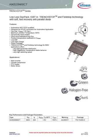
aikp20n60ct.pdf
AIKP20N60CT TRENCHSTOPTM Series Low Loss DuoPack IGBT in TRENCHSTOPTM and Fieldstop technology with soft, fast recovery anti-parallel Emitter Controlled diode C Features Automotive AEC Q101 qualified Designed for DC/AC converters for Automotive Application Very low V 1.5V (typ.) CE(sat) Maximum Junction Temperature 150 C G Dynamically stress tested E Sho
sgp20n60.pdf

SGP20N60 SGW20N60 Fast IGBT in NPT-technology C 75% lower Eoff compared to previous generation combined with low conduction losses Short circuit withstand time 10 s G Designed for E - Motor controls - Inverter NPT-Technology for 600V applications offers - very tight parameter distribution - high ruggedness, temperature stable behaviour - paral
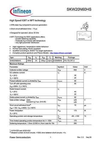
skw20n60hs.pdf

SKW20N60HS High Speed IGBT in NPT-technology C 30% lower Eoff compared to previous generation Short circuit withstand time 10 s G E Designed for operation above 30 kHz NPT-Technology for 600V applications offers - parallel switching capability PG-TO-247-3-21 - moderate Eoff increase with temperature - very tight parameter distribution High ruggednes
spa20n60cfd.pdf
SPA20N60CFD CoolMOSTM Power Transistor Product Summary Features V 600 V DS New revolutionary high voltage technology R 0.22 DS(on),max Intrinsic fast-recovery body diode 1) 20.7 A I D Extremely low reverse recovery charge Ultra low gate charge PG-TO220-3-31 Extreme dv /dt rated High peak current capability Periodic avalanche rated Qualified f
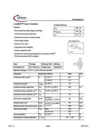
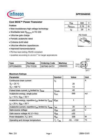
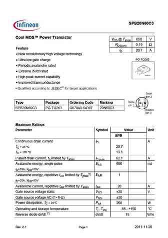
spb20n60s5.pdf
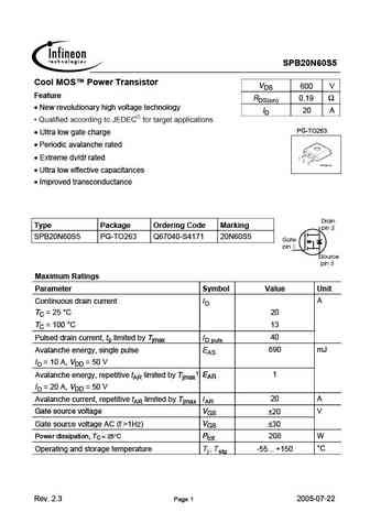
SPB20N60S5 Cool MOS Power Transistor VDS 600 V Feature RDS(on) 0.19 New revolutionary high voltage technology ID 20 A PG-TO263 Ultra low gate charge Periodic avalanche rated Extreme dv/dt rated Ultra low effective capacitances Improved transconductance Type Package Ordering Code Marking SPB20N60S5 PG-TO263 Q67040-S4171 20N60S5 Maximum Ratings Para
sgp20n60hs.pdf
SGP20N60HS SGW20N60HS High Speed IGBT in NPT-technology C 30% lower Eoff compared to previous generation Short circuit withstand time 10 s G E Designed for operation above 30 kHz NPT-Technology for 600V applications offers - parallel switching capability PG-TO-220-3-1 PG-TO-247-3 - moderate Eoff increase with temperature - very tight parameter distri
skw20n60hsg.pdf
SKW20N60HS High Speed IGBT in NPT-technology C 30% lower Eoff compared to previous generation Short circuit withstand time 10 s G E Designed for operation above 30 kHz NPT-Technology for 600V applications offers - parallel switching capability PG-TO-247-3 - moderate Eoff increase with temperature - very tight parameter distribution High ruggedness,
sgp20n60 sgw20n60 rev2 4g.pdf

SGP20N60 SGW20N60 Fast IGBT in NPT-technology C 75% lower Eoff compared to previous generation combined with low conduction losses Short circuit withstand time 10 s G Designed for E - Motor controls - Inverter NPT-Technology for 600V applications offers - very tight parameter distribution - high ruggedness, temperature stable behaviour - paral
spp20n60s5.pdf
SPP20N60S5 Final data SPB20N60S5 Cool MOS Power Transistor VDS 600 V Feature RDS(on) 0.19 New revolutionary high voltage technology ID 20 A Worldwide best RDS(on) in TO 220 P-TO263-3-2 P-TO220-3-1 Ultra low gate charge Periodic avalanche rated Extreme dv/dt rated Ultra low effective capacitances Improved noise immunity Type Package Ordering Cod
aikq120n60ct.pdf
AIKQ120N60CT TRENCHSTOPTM Series Low Loss DuoPack IGBT in TRENCHSTOPTM and Fieldstop technology with soft, fast recovery antiparallel Emitter Controlled diode C Features Automotive AEC-Q101 qualified Designed for DC/AC converters for Automotive Application Very low V 1.5V (typ.) CE(sat) Maximum junction temperature 175 C G Dynamically stress tested E Sho
ikq120n60t.pdf
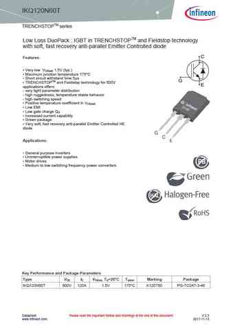
IKQ120N60T TRENCHSTOPTM series Low Loss DuoPack IGBT in TRENCHSTOPTM and Fieldstop technology with soft, fast recovery anti-parallel Emitter Controlled diode C Features Very low V 1.5V (typ.) CE(sat) Maximum junction temperature 175 C Short circuit withstand time 5 s G TRENCHSTOPTM and Fieldstop technology for 600V E applications offers - very tight parameter
ikp20n60t.pdf
IKP20N60T TRENCHSTOP Series Low Loss DuoPack IGBT in TRENCHSTOP and Fieldstop technology with soft, fast recovery anti-parallel Emitter Controlled HE diode C Features Very low VCE(sat) 1.5V (typ.) Maximum Junction Temperature 175 C G Short circuit withstand time 5 s E Designed for - Frequency Converters - Uninterrupted Power Supply
aikw20n60ct.pdf
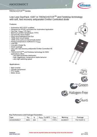
AIKW20N60CT TRENCHSTOPTM Series Low Loss DuoPack IGBT in TRENCHSTOPTM and Fieldstop technology with soft, fast recovery antiparallel Emitter Controlled diode C Features Automotive AEC-Q101 qualified Designed for DC/AC converters for Automotive Application Very low V 1.5V (typ.) CE(sat) Maximum junction temperature 175 C G Dynamically stress tested E Shor
spp20n60s5 .pdf
SPP20N60S5 Cool MOS Power Transistor VDS 600 V Feature RDS(on) 0.19 New revolutionary high voltage technology ID 20 A Worldwide best RDS(on) in TO 220 PG-TO220 Ultra low gate charge 2 Periodic avalanche rated Extreme dv/dt rated 3 2 1 Ultra low effective capacitances P-TO220-3-1 Improved transconductance Type Package Ordering Code Marking
spp20n60cfd.pdf
SPP20N60CFD C I MOS P wer Transist r VDS @ Tjmax 650 V Feature RDS(on) 0.22 New revolutionary high voltage technology ID 20.7 A Worldwide best RDS(on) in TO 220 PG-TO220 Ultra low gate charge Periodic avalanche rated Extreme dv/dt rated High peak current capability Intrinsic fast-recovery body diode Extreme low reverse recovery charge Type Pa

sgb20n60 .pdf
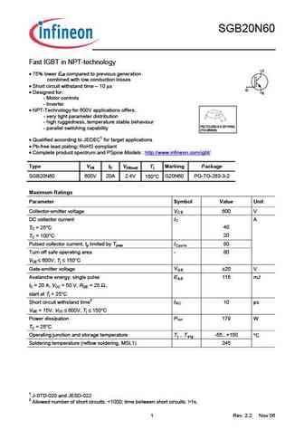
SGB20N60 Fast IGBT in NPT-technology C 75% lower Eoff compared to previous generation combined with low conduction losses Short circuit withstand time 10 s G Designed for E - Motor controls - Inverter NPT-Technology for 600V applications offers - very tight parameter distribution - high ruggedness, temperature stable behaviour PG-TO-263-3-2 (D
spw20n60s5.pdf
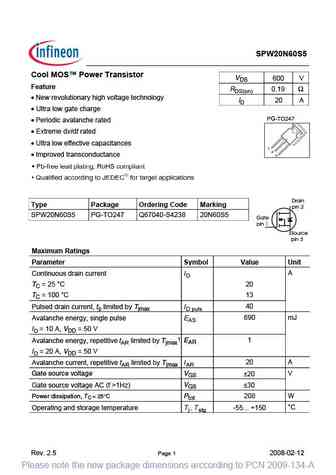
SPW20N60S5 Cool MOS Power Transistor VDS 600 V Feature RDS(on) 0.19 New revolutionary high voltage technology ID 20 A Ultra low gate charge PG-TO247 Periodic avalanche rated Extreme dv/dt rated Ultra low effective capacitances Improved transconductance Type Package Ordering Code Marking SPW20N60S5 PG-TO247 Q67040-S4238 20N60S5 Maximum Ratings Para

ikb20n60t.pdf
IKB20N60T TRENCHSTOP Series p Low Loss DuoPack IGBT in TRENCHSTOP and Fieldstop technology with soft, fast recovery anti-parallel Emitter Controlled HE diode Features C Very low VCE(sat) 1.5V (typ.) Maximum Junction Temperature 175 C Short circuit withstand time 5 s Designed for frequency inverters for washing machines, fans, pumps and vacuum G
sgp20n60 sgw20n60 rev2.pdf
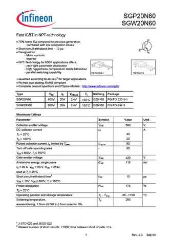
SGP20N60 SGW20N60 Fast IGBT in NPT-technology C 75% lower Eoff compared to previous generation combined with low conduction losses Short circuit withstand time 10 s G Designed for E - Motor controls - Inverter NPT-Technology for 600V applications offers - very tight parameter distribution - high ruggedness, temperature stable behaviour - paral
ikq120n60ta.pdf
IGBT Low Loss DuoPack IGBT in TRENCHSTOPTM and Fieldstop technology with soft, fast recovery antiparallel Emitter Controlled diode IKQ120N60TA 600V low loss switching series third generation Data sheet Industrial Power Control IKQ120N60TA TRENCHSTOPTM series Low Loss DuoPack IGBT in TRENCHSTOPTM and Fieldstop technology with soft, fast recovery antiparallel Emitter Controlled di
ikb20n60trev2 4g.pdf
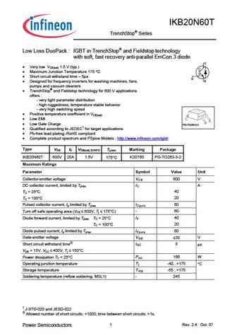
IKB20N60T TrenchStop Series p Low Loss DuoPack IGBT in TrenchStop and Fieldstop technology with soft, fast recovery anti-parallel EmCon 3 diode C Very low VCE(sat) 1.5 V (typ.) Maximum Junction Temperature 175 C Short circuit withstand time 5 s G E Designed for frequency inverters for washing machines, fans, pumps and vacuum cleaners Trench
ikw20n60h3.pdf

IGBT High speed DuoPack IGBT in Trench and Fieldstop technology with soft, fast recovery anti-parallel diode IKW20N60H3 600V high speed switching series third generation Data sheet Industrial Power Control IKW20N60H3 High speed switching series third generation High speed DuoPack IGBT in Trench and Fieldstop technology with soft, fast recovery anti-parallel diode C Features TRE
ikw20n60h3 rev1 2g.pdf
IGBT High speed DuoPack IGBT in Trench and Fieldstop technology with soft, fast recovery anti-parallel diode IKW20N60H3 600V high speed switching series third generation Datasheet Industrial & Multimarket IKW20N60H3 High speed switching series third generation High speed DuoPack IGBT in Trench and Fieldstop technology with soft, fast recovery anti-parallel diode C Features TREN
spw20n60cfd.pdf
Please note the new package dimensions arccording to PCN 2009 1 4 A Please note the new package dimensions arccording to PCN 2009 1 4 A Please note the new package dimensions arccording to PCN 2009 1 4 A Please note the new package dimensions arccording to PCN 2009 1 4 A Please note the new package dimensions arccording to PCN 2009 1 4 A Please note the new package
igp20n60h3.pdf
IGBT High speed IGBT in Trench and Fieldstop technology IGP20N60H3 600V high speed switching series third generation Data sheet Industrial Power Control IGP20N60H3 High speed switching series third generation High speed IGBT in Trench and Fieldstop technology Features C TRENCHSTOPTM technology offering very low turn-off energy low V CEsat low EMI maximum junctio
sgp20n60hs sgw20n60hs rev2.pdf

SGP20N60HS SGW20N60HS High Speed IGBT in NPT-technology C 30% lower Eoff compared to previous generation Short circuit withstand time 10 s G E Designed for operation above 30 kHz NPT-Technology for 600V applications offers - parallel switching capability PG-TO-220-3-1 PG-TO-247-3 - moderate Eoff increase with temperature - very tight parameter distri
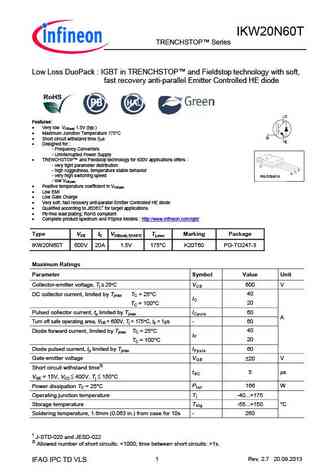
ikp20n60t ikw20n60t rev2 5g.pdf
IKP20N60T TrenchStop Series IKW20N60T Low Loss DuoPack IGBT in TrenchStop and Fieldstop technology with soft, fast recovery anti-parallel EmCon HE diode C Very low VCE(sat) 1.5 V (typ.) Maximum Junction Temperature 175 C Short circuit withstand time 5 s G E Designed for - Frequency Converters - Uninterrupted Power Supply TrenchStop an
spp20n60c3 spi20n60c3 spa20n60c3 spp20n60c3 spi20n60c3 spa20n60c3 rev3.2.pdf
SPP20N60C3 SPI20N60C3, SPA20N60C3 Cool MOS Power Transistor VDS @ Tjmax 650 V Feature RDS(on) 0.19 New revolutionary high voltage technology ID 20.7 A Worldwide best RDS(on) in TO 220 PG-TO220FP PG-TO262 PG-TO220 Ultra low gate charge Periodic avalanche rated 3 Extreme dv/dt rated 2 1 P-TO220-3-31 High peak current capability Improved transco
skw20n60g.pdf
SKW20N60 Fast IGBT in NPT-technology with soft, fast recovery anti-parallel EmCon diode C 75% lower Eoff compared to previous generation combined with low conduction losses Short circuit withstand time 10 s G E Designed for - Motor controls - Inverter NPT-Technology for 600V applications offers - very tight parameter distribution - high ruggedness,

ikw20n60t.pdf
IKW20N60T TRENCHSTOP Series Low Loss DuoPack IGBT in TRENCHSTOP and Fieldstop technology with soft, fast recovery anti-parallel Emitter Controlled HE diode C Features Very low VCE(sat) 1.5V (typ.) Maximum Junction Temperature 175 C G Short circuit withstand time 5 s E Designed for - Frequency Converters - Uninterrupted Power Supply TRENCHSTOP a
igb20n60h3.pdf

IGBT High speed IGBT in Trench and Fieldstop technology IGB20N60H3 600V high speed switching series third generation Data sheet Industrial Power Control IGB20N60H3 High speed switching series third generation High speed IGBT in Trench and Fieldstop technology Features C TRENCHSTOPTM technology offering very low turn-off energy low V CEsat low EMI maximum junctio
aikb20n60ct.pdf
AIKB20N60CT TRENCHSTOPTM Series Low Loss DuoPack IGBT in TRENCHSTOPTM and Fieldstop technology with soft, fast recovery anti-parallel diode C Features Automotive AEC Q101 qualified Designed for DC/AC converters for Automotive Application Very low V 1.5V (typ.) CE(sat) Maximum Junction Temperature 150 C G Dynamically stress tested E Short circuit withstan
sgw20n60hs.pdf
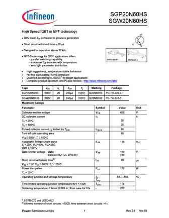
SGP20N60HS SGW20N60HS High Speed IGBT in NPT-technology C 30% lower Eoff compared to previous generation Short circuit withstand time 10 s G E Designed for operation above 30 kHz NPT-Technology for 600V applications offers - parallel switching capability PG-TO-220-3-1 PG-TO-247-3 - moderate Eoff increase with temperature - very tight parameter distri
sgb20n60.pdf

SGB20N60 Fast IGBT in NPT-technology C 75% lower Eoff compared to previous generation combined with low conduction losses Short circuit withstand time 10 s G Designed for E - Motor controls - Inverter NPT-Technology for 600V applications offers - very tight parameter distribution - high ruggedness, temperature stable behaviour PG-TO-263-3-2 (D
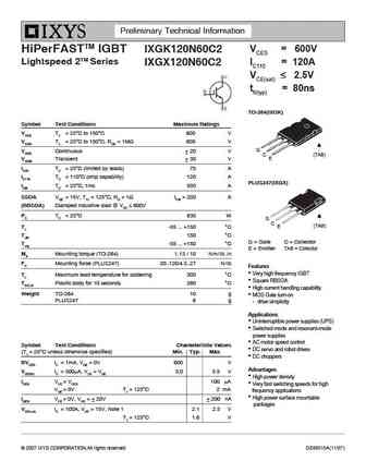
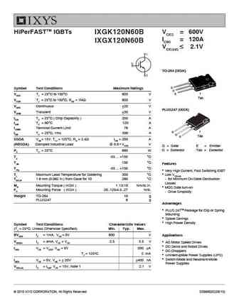
ixgk120n60c2.pdf
Preliminary Technical Information VCES = 600V HiPerFASTTM IGBT IXGK120N60C2 Lightspeed 2TM Series IC110 = 120A IXGX120N60C2 VCE(sat) 2.5V tfi(typ) = 80ns TO-264(IXGK) Symbol Test Conditions Maximum Ratings VCES TJ = 25 C to 150 C 600 V VCGR TJ = 25 C to 150 C, RGE = 1M 600 V G VGES Continuous 20 V C (TAB) E VGEM Transient 30 V IC25 TC = 25
ixgp20n60b.pdf
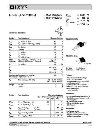
IXGA 20N60B VCES = 600 V HiPerFASTTM IGBT IXGP 20N60B IC25 = 40 A VCE(sat)typ = 1.7 V tfi = 100 ns Preliminary data sheet Symbol Test Conditions Maximum Ratings TO-220AB (IXGP) VCES TJ = 25 C to 150 C 600 V VCGR TJ = 25 C to 150 C; RGE = 1 MW 600 V VGES Continuous 20 V G VGEM Transient 30 V C E IC25 TC = 25 C 40 A IC90 TC = 90 C 20 A TO-263 AA (IXGA) ICM TC = 25 C,
ixkc20n60c.pdf
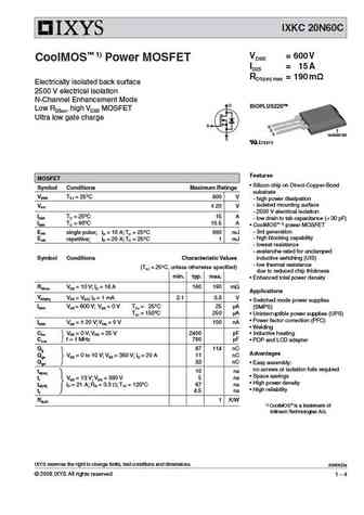
IXKC 20N60C VDSS = 600 V CoolMOS 1) Power MOSFET ID25 = 15 A RDS(on) max = 190 m Electrically isolated back surface 2500 V electrical isolation N-Channel Enhancement Mode D ISOPLUS220TM Low RDSon, high VDSS MOSFET Ultra low gate charge G G D S isolated tab S E72873 Features MOSFET Silicon chip on Direct-Copper-Bond Symbol Conditions Maximum Ratings substrate
ixth15n60 ixtm15n60 ixth20n60 ixtm20n60.pdf
Downloaded from DatasheetLib.com - datasheet search engine Downloaded from DatasheetLib.com - datasheet search engine Downloaded from DatasheetLib.com - datasheet search engine Downloaded from DatasheetLib.com - datasheet search engine
ixgk120n60b3-ixgx120n60b3.pdf
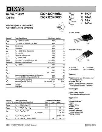
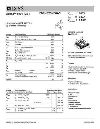
VCES = 600V GenX3TM 600V IXGK120N60B3 IC110 = 120A IXGX120N60B3 IGBTs VCE(sat) 1.8V tfi(typ) = 145ns Medium-Speed-Low-Vsat PT IGBTs for 5-40kHz Switching TO-264 (IXGK) Symbol Test Conditions Maximum Ratings G VCES TJ = 25 C to 150 C 600 V C E VCGR TJ = 25 C to 150 C, RGE = 1M 600 V Tab VGES Continuous 20 V VGEM Transient 30 V PLUS247TM (IXG
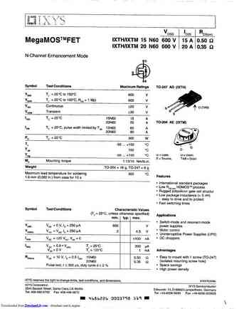
ixth20n60 ixtm20n60.pdf
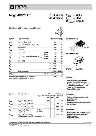
IXTH 20N60 VDSS = 600 V MegaMOSTMFET IXTM 20N60 ID25 = 20 A RDS(on) = 0.35 N-Channel Enhancement Mode Symbol Test Conditions Maximum Ratings TO-247 AD (IXTH) VDSS TJ = 25 C to 150 C 600 V VDGR TJ = 25 C to 150 C; RGS = 1 M 600 V VGS Continuous 20 V D (TAB) VGSM Transient 30 V ID25 TC = 25 C 15N60 15 A TO-204 AE (IXTM) 20N60 20 A IDM TC = 25 C, p
ixgx120n60b3.pdf

VCES = 600V GenX3TM 600V IXGK120N60B3 IC110 = 120A IXGX120N60B3 IGBTs VCE(sat) 1.8V tfi(typ) = 145ns Medium-Speed-Low-Vsat PT IGBTs for 5-40kHz Switching TO-264 (IXGK) Symbol Test Conditions Maximum Ratings G VCES TJ = 25 C to 150 C 600 V C E VCGR TJ = 25 C to 150 C, RGE = 1M 600 V Tab VGES Continuous 20 V VGEM Transient 30 V PLUS247TM (IXG
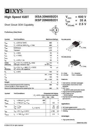
ixsp20n60b2 ixsp20n60b2d1.pdf
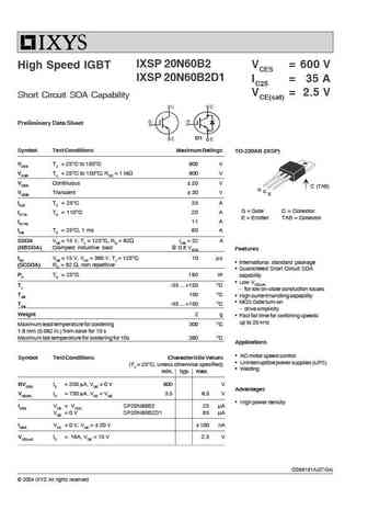
IXSP 20N60B2 VCES = 600 V High Speed IGBT IXSP 20N60B2D1 IC25 = 35 A VCE(sat) = 2.5 V Short Circuit SOA Capability Preliminary Data Sheet D1 Symbol Test Conditions Maximum Ratings TO-220AB (IXSP) VCES TJ = 25 C to 150 C 600 V VCGR TJ = 25 C to 150 C; RGE = 1 M 600 V VGES Continuous 20 V C (TAB) G C VGEM Transient 30 V E IC25 TC = 25 C35 A G = Gate C = Collector
ixgx120n60a3.pdf

GenX3TM A3-Class IXGK120N60A3 VCES = 600V IXGX120N60A3 IC110 = 120A IGBTS VCE(sat) 1.35V Ultra-Low Vsat PT IGBTs for up to 5kHz Switching TO-264 (IXGK) Symbol Test Conditions Maximum Ratings VCES TJ = 25 C to 150 C 600 V VCGR TJ = 25 C to 150 C, RGE = 1M 600 V G (TAB) C VGES Continuous 20 V E E VGEM Transient 30 V IC25 TC = 25 C 200 A PLUS 2
ixgk320n60b3.pdf
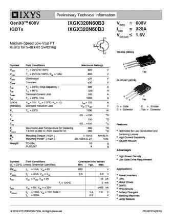
Preliminary Technical Information GenX3TM 600V VCES = 600V IXGK320N60B3 IC90 = 320A IGBTs IXGX320N60B3 VCE(sat) 1.6V Medium-Speed Low-Vsat PT IGBTs for 5-40 kHz Switching TO-264 (IXGK) G Symbol Test Conditions Maximum Ratings C E VCES TJ = 25 C to 150 C 600 V Tab VCGR TJ = 25 C to 150 C, RGE = 1M 600 V VGES Continuous 20 V PLUS247 (IXGX) VGEM T
ixgk120n60c2 ixgx120n60c2.pdf
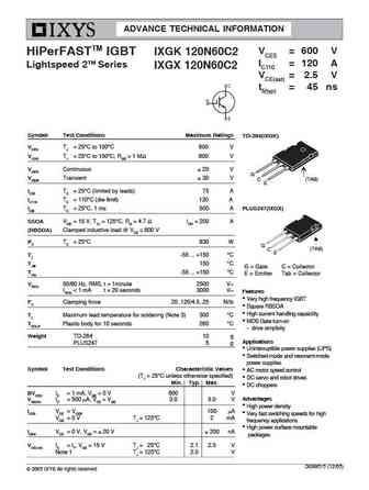
ADVANCE TECHNICAL INFORMATION VCES = 600 V HiPerFASTTM IGBT IXGK 120N60C2 IC110 = 120 A Lightspeed 2TM Series IXGX 120N60C2 VCE(sat) = 2.5 V tfi(typ) = 45 ns Symbol Test Conditions Maximum Ratings TO-264(IXGK) VCES TJ = 25 C to 150 C 600 V VCGR TJ = 25 C to 150 C; RGE = 1 M 600 V VGES Continuous 20 V G VGEM Transient 30 V C (TAB) E IC25 TC = 25 C (limited by leads)
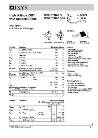
ixdp20n60b.pdf

IXDP 20N60 B VCES = 600 V High Voltage IGBT IXDP 20N60 BD1 IC25 = 32 A with optional Diode VCE(sat) typ = 2.2 V High Speed, Low Saturation Voltage C C TO-220 AB G G G C E C (TAB) E E G = Gate, E = Emitter IXDP 20N60B IXDP 20N60B D1 C = Collector , TAB = Collector Symbol Conditions Maximum Ratings Features NPT IGBT technology VCES TJ = 25 C to 150 C 600 V low switching l
ixgk120n60a3.pdf
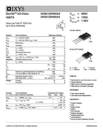
GenX3TM A3-Class IXGK120N60A3 VCES = 600V IXGX120N60A3 IC110 = 120A IGBTS VCE(sat) 1.35V Ultra-Low Vsat PT IGBTs for up to 5kHz Switching TO-264 (IXGK) Symbol Test Conditions Maximum Ratings VCES TJ = 25 C to 150 C 600 V VCGR TJ = 25 C to 150 C, RGE = 1M 600 V G (TAB) C VGES Continuous 20 V E E VGEM Transient 30 V IC25 TC = 25 C 200 A PLUS 2
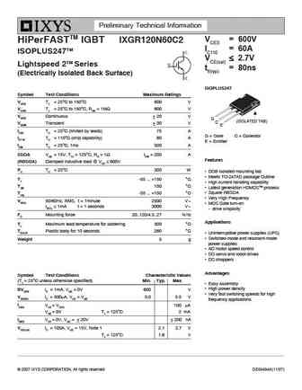
ixgr120n60b.pdf
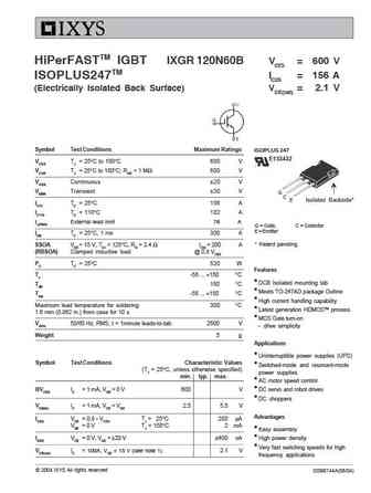
HiPerFASTTM IGBT IXGR 120N60B VCES = 600 V IC25 = 156 A ISOPLUS247TM (Electrically Isolated Back Surface) VCE(sat) = 2.1 V Symbol Test Conditions Maximum Ratings ISOPLUS 247 E153432 VCES TJ = 25 C to 150 C 600 V VCGR TJ = 25 C to 150 C; RGE = 1 M 600 V VGES Continuous 20 V VGEM Transient 30 V G C E Isolated Backside* IC25 TC = 25 C 156 A IC110 TC = 110 C 102 A IL(R
ixsh20n60u1.pdf
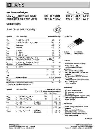
Not for new designs VCES IC25 VCE(sat) Low VCE(sat) IGBT with Diode IXSH 20 N60U1 600 V 40 A 2.5 V High Speed IGBT with Diode IXSH 20 N60AU1 600 V 40 A 3.0 V Combi Packs Short Circuit SOA Capability Symbol Test Conditions Maximum Ratings TO-247 AD VCES TJ = 25 C to 150 C 600 V VCGR TJ = 25 C to 150 C; RGE = 1 M 600 V VGES Continuous 20 V G C VGEM Transient 30 V E IC25 TC
ixgk120n60b ixgx120n60b.pdf
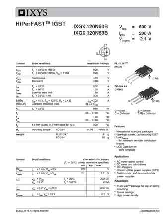
HiPerFASTTM IGBT IXGK 120N60B VCES = 600 V IXGX 120N60B IC25 = 200 A VCE(sat) = 2.1 V Symbol Test Conditions Maximum Ratings PLUS 247TM (IXGX) VCES TJ = 25 C to 150 C 600 V VCGR TJ = 25 C to 150 C; RGS = 1 M 600 V VCES Continuous 20 V (TAB) G VGEM Transient 30 V C E IC25 TC = 25 C 200 A TO-264 AA IC90 TC = 90 C 120 A (IXGK) IL(RMS) External lead limit 76 A ICM TC
ixgh20n60-a ixgm20n60-a.pdf
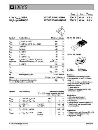
VCES IC25 VCE(sat) Low VCE(sat) IGBT IXGH/IXGM 20 N60 600 V 40 A 2.5 V High speed IGBT IXGH/IXGM 20 N60A 600 V 40 A 3.0 V Symbol Test Conditions Maximum Ratings TO-247 AD (IXGH) VCES TJ = 25 C to 150 C 600 V VCGR TJ = 25 C to 150 C; RGE = 1 M 600 V VGES Continuous 20 V G C VGEM Transient 30 V E IC25 TC = 25 C40 A IC90 TC = 90 C20 A TO-204 AE (IXGM) ICM TC = 25 C, 1 ms
ixgk320n60a3.pdf
GenX3TM 600V IGBTs VCES = 600V IXGK320N60A3 IC25 = 320A IXGX320N60A3 VCE(sat) 1.25V Ultra-Low Vsat PT IGBTs for up to 5kHz Switching TO-264 (IXGK) Symbol Test Conditions Maximum Ratings VCES TJ = 25 C to 150 C 600 V G VCGR TJ = 25 C to 150 C, RGE = 1M 600 V C Tab E E VGES Continuous 20 V VGEM Transient 30 V PLUS247TM (IXGX) IC25 TC = 25 C (C
mmix1g320n60b3.pdf
Advance Technical Information GenX3TM 600V VCES = 600V MMIX1G320N60B3 IC25 = 400A IGBT VCE(sat) 1.50V Medium-Speed Low-Vsat PT IGBTs for 5-40 kHz Switching C G E Symbol Test Conditions Maximum Ratings VCES TJ = 25 C to 150 C 600 V Isolated Tab VCGR TJ = 25 C to 150 C, RGE = 1M 600 V C VGES Continuous 20 V VGEM Transient 30 V IC25 TC = 25 C 4
ixgn120n60a3.pdf
VCES = 600V IXGN120N60A3 GenX3TM 600V IGBT IXGN120N60A3D1 IC110 = 120A VCE(sat) 1.35V Ultra-low Vsat PT IGBTs for up to 5kHz switching SOT-227B, miniBLOC E153432 E E 60A3 60A3D1 G Symbol Test Conditions Maximum Ratings VCES TJ = 25 C to 150 C 600 V E VCGR TJ = 25 C to 150 C, RGE = 1M 600 V C VGES Continuous 20 V G = Gate, C = Collector, E =
ixgn120n60a3d1.pdf

VCES = 600V IXGN120N60A3 GenX3TM 600V IGBT IXGN120N60A3D1 IC110 = 120A VCE(sat) 1.35V Ultra-low Vsat PT IGBTs for up to 5kHz switching SOT-227B, miniBLOC E153432 E E 60A3 60A3D1 G Symbol Test Conditions Maximum Ratings VCES TJ = 25 C to 150 C 600 V E VCGR TJ = 25 C to 150 C, RGE = 1M 600 V C VGES Continuous 20 V G = Gate, C = Collector, E =
ixgk120n60b3.pdf

VCES = 600V GenX3TM 600V IXGK120N60B3 IC110 = 120A IXGX120N60B3 IGBTs VCE(sat) 1.8V tfi(typ) = 145ns Medium-Speed-Low-Vsat PT IGBTs for 5-40kHz Switching TO-264 (IXGK) Symbol Test Conditions Maximum Ratings G VCES TJ = 25 C to 150 C 600 V C E VCGR TJ = 25 C to 150 C, RGE = 1M 600 V Tab VGES Continuous 20 V VGEM Transient 30 V PLUS247TM (IXG
ixsh20n60b2d1.pdf
IXSH 20N60B2D1 VCES = 600 V High Speed IGBT IC25 = 35 A VCE(sat) = 2.5 V Short Circuit SOA Capability Preliminary Data Sheet D1 Symbol Test Conditions Maximum Ratings TO-247 (IXSH) VCES TJ = 25 C to 150 C 600 V VCGR TJ = 25 C to 150 C; RGE = 1 M 600 V VGES Continuous 20 V G VGEM Transient 30 V C E IC25 TC = 25 C35 A G = Gate C = Collector IC110 TC = 110 C20 A E
ixgk120n60b.pdf
HiPerFASTTM IGBTs VCES = 600V IXGK120N60B IC90 = 120A IXGX120N60B VCE(sat) 2.1V TO-264 (IXGK) G Symbol Test Conditions Maximum Ratings C E VCES TJ = 25 C to 150 C 600 V Tab VCGR TJ = 25 C to 150 C, RGE = 1M 600 V VGES Continuous 20 V PLUS247 (IXGX) VGEM Transient 30 V IC25 TC = 25 C ( Chip Capability ) 200 A IC90 TC = 90 C 120 A ILRMS Termin
ixfh20n60q ixft20n60q.pdf
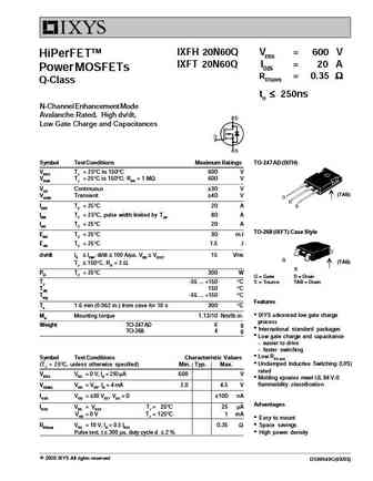
IXFH 20N60Q VDSS = 600 V HiPerFETTM IXFT 20N60Q ID25 = 20 A Power MOSFETs RDS(on) = 0.35 Q-Class trr 250ns N-Channel Enhancement Mode Avalanche Rated, High dv/dt, Low Gate Charge and Capacitances Symbol Test Conditions Maximum Ratings TO-247 AD (IXFH) VDSS TJ = 25 C to 150 C 600 V VDGR TJ = 25 C to 150 C; RGS = 1 M 600 V VGS C
ixfh15n60 ixfh20n60 ixfm15n60 ixfm20n60.pdf
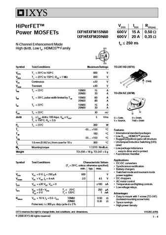
VDSS ID25 RDS(on) HiPerFETTM IXFH/IXFM 15 N60 600 V 15 A 0.50 W Power MOSFETs IXFH/IXFM 20 N60 600 V 20 A 0.35 W trr 250 ns N-Channel Enhancement Mode High dv/dt, Low trr, HDMOSTM Family Symbol Test Conditions Maximum Ratings TO-247 AD (IXFH) VDSS TJ = 25 C to 150 C 600 V VDGR TJ = 25 C to 150 C; RGS = 1 MW 600 V (TAB) VGS Continuous 20 V VGSM Transient 30 V ID25 TC = 2
ixgx320n60b3.pdf

Preliminary Technical Information GenX3TM 600V VCES = 600V IXGK320N60B3 IC90 = 320A IGBTs IXGX320N60B3 VCE(sat) 1.6V Medium-Speed Low-Vsat PT IGBTs for 5-40 kHz Switching TO-264 (IXGK) G Symbol Test Conditions Maximum Ratings C E VCES TJ = 25 C to 150 C 600 V Tab VCGR TJ = 25 C to 150 C, RGE = 1M 600 V VGES Continuous 20 V PLUS247 (IXGX) VGEM T
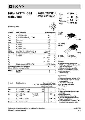
ixgt20n60b.pdf
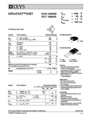
VCES = 600 V IXGH 20N60B HiPerFASTTM IGBT IC25 = 40 A IXGT 20N60B VCE(sat)typ = 1.7 V tfi(typ) = 100 ns Preliminary data sheet Symbol Test Conditions Maximum Ratings TO-268 (D3) (IXGT) VCES TJ = 25 C to 150 C 600 V VCGR TJ = 25 C to 150 C; RGE = 1 MW 600 V G (TAB) E VGES Continuous 20 V VGEM Transient 30 V IC25 TC = 25 C40 A TO-247 AD (IXGH) IC90 TC = 90 C20 A ICM T
ixsp20n60b2d1.pdf
IXSA 20N60B2D1 VCES = 600 V High Speed IGBT IXSP 20N60B2D1 IC25 = 35 A VCE(sat) = 2.5 V Short Circuit SOA Capability Preliminary Data Sheet Symbol Test Conditions Maximum Ratings TO-220 (IXSP) VCES TJ = 25 C to 150 C 600 V VCGR TJ = 25 C to 150 C; RGE = 1 M 600 V C (TAB) VGES Continuous 20 V G C VGEM Transient 30 V E IC25 TC = 25 C35 A IC110 TC = 110 C20 A TO-22
ixgn120n60a3-a3d1.pdf

VCES = 600V IXGN120N60A3 GenX3TM 600V IGBT IXGN120N60A3D1 IC110 = 120A VCE(sat) 1.35V Ultra-low Vsat PT IGBTs for up to 5kHz switching SOT-227B, miniBLOC E153432 E E 60A3 60A3D1 G Symbol Test Conditions Maximum Ratings VCES TJ = 25 C to 150 C 600 V E VCGR TJ = 25 C to 150 C, RGE = 1M 600 V C VGES Continuous 20 V G = Gate, C = Collector, E =
ixsq20n60b2d1.pdf

IXSH 20N60B2D1 VCES = 600 V High Speed IGBT IC25 = 35 A VCE(sat) = 2.5 V Short Circuit SOA Capability Preliminary Data Sheet D1 Symbol Test Conditions Maximum Ratings TO-247 (IXSH) VCES TJ = 25 C to 150 C 600 V VCGR TJ = 25 C to 150 C; RGE = 1 M 600 V VGES Continuous 20 V G VGEM Transient 30 V C E IC25 TC = 25 C35 A G = Gate C = Collector IC110 TC = 110 C20 A E
ixgx120n60c2.pdf

Preliminary Technical Information VCES = 600V HiPerFASTTM IGBT IXGK120N60C2 Lightspeed 2TM Series IC110 = 120A IXGX120N60C2 VCE(sat) 2.5V tfi(typ) = 80ns TO-264(IXGK) Symbol Test Conditions Maximum Ratings VCES TJ = 25 C to 150 C 600 V VCGR TJ = 25 C to 150 C, RGE = 1M 600 V G VGES Continuous 20 V C (TAB) E VGEM Transient 30 V IC25 TC = 25
ixga20n60b.pdf

IXGA 20N60B VCES = 600 V HiPerFASTTM IGBT IXGP 20N60B IC25 = 40 A VCE(sat)typ = 1.7 V tfi = 100 ns Preliminary data sheet Symbol Test Conditions Maximum Ratings TO-220AB (IXGP) VCES TJ = 25 C to 150 C 600 V VCGR TJ = 25 C to 150 C; RGE = 1 MW 600 V VGES Continuous 20 V G VGEM Transient 30 V C E IC25 TC = 25 C 40 A IC90 TC = 90 C 20 A TO-263 AA (IXGA) ICM TC = 25 C,
ixgx120n60b.pdf

HiPerFASTTM IGBTs VCES = 600V IXGK120N60B IC90 = 120A IXGX120N60B VCE(sat) 2.1V TO-264 (IXGK) G Symbol Test Conditions Maximum Ratings C E VCES TJ = 25 C to 150 C 600 V Tab VCGR TJ = 25 C to 150 C, RGE = 1M 600 V VGES Continuous 20 V PLUS247 (IXGX) VGEM Transient 30 V IC25 TC = 25 C ( Chip Capability ) 200 A IC90 TC = 90 C 120 A ILRMS Termin
ixgr120n60c2.pdf
Preliminary Technical Information VCES = 600V HiPerFASTTM IGBT IXGR120N60C2 IC110 = 60A ISOPLUS247TM VCE(sat) 2.7V Lightspeed 2TM Series tfi(typ) = 80ns (Electrically Isolated Back Surface) ISOPLUS247 Symbol Test Conditions Maximum Ratings VCES TJ = 25 C to 150 C 600 V VCGR TJ = 25 C to 150 C, RGE = 1M 600 V VGES Continuous 20 V G (ISOLATED TAB)
ixdp20n60bd1.pdf
IXDP 20N60 B VCES = 600 V High Voltage IGBT IXDP 20N60 BD1 IC25 = 32 A with optional Diode VCE(sat) typ = 2.2 V High Speed, Low Saturation Voltage C C TO-220 AB G G G C E C (TAB) E E G = Gate, E = Emitter IXDP 20N60B IXDP 20N60B D1 C = Collector , TAB = Collector Symbol Conditions Maximum Ratings Features NPT IGBT technology VCES TJ = 25 C to 150 C 600 V low switching l
ixkp20n60c5m.pdf
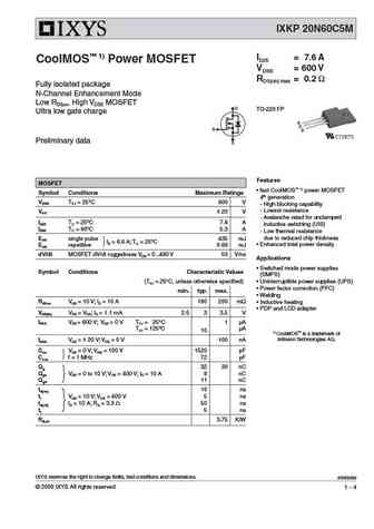
IXKP 20N60C5M ID25 = 7.6 A CoolMOS 1) Power MOSFET VDSS = 600 V RDS(on) max = 0.2 Fully isolated package N-Channel Enhancement Mode Low RDSon, High VDSS MOSFET D TO-220 FP Ultra low gate charge G D G S Preliminary data S Features MOSFET fast CoolMOS 1) power MOSFET Symbol Conditions Maximum Ratings 4th generation VDSS TVJ = 25 C 600 V - High blocking capabi
ixgt20n60bd1.pdf
IXGH 20N60BD1 HiPerFASTTM IGBT VCES = 600 V IXGT 20N60BD1 with Diode IC25 = 40 A VCE(sat)typ = 1.7 V tfi(typ) = 100 ns Preliminary data Symbol Test Conditions Maximum Ratings TO-268 (IXGT) VCES TJ = 25 C to 150 C 600 V G VCGR TJ = 25 C to 150 C; RGE = 1 MW 600 V E C (TAB) VGES Continuous 20 V VGEM Transient 30 V TO-247 AD IC25 TC = 25 C40 A (IXGH) IC90 TC = 90 C20 A
ixgh20n60bd1.pdf

IXGH 20N60BD1 HiPerFASTTM IGBT VCES = 600 V IXGT 20N60BD1 with Diode IC25 = 40 A VCE(sat)typ = 1.7 V tfi(typ) = 100 ns Preliminary data Symbol Test Conditions Maximum Ratings TO-268 (IXGT) VCES TJ = 25 C to 150 C 600 V G VCGR TJ = 25 C to 150 C; RGE = 1 MW 600 V E C (TAB) VGES Continuous 20 V VGEM Transient 30 V TO-247 AD IC25 TC = 25 C40 A (IXGH) IC90 TC = 90 C20 A
ixsh20n60au1.pdf

Not for new designs VCES IC25 VCE(sat) Low VCE(sat) IGBT with Diode IXSH 20 N60U1 600 V 40 A 2.5 V High Speed IGBT with Diode IXSH 20 N60AU1 600 V 40 A 3.0 V Combi Packs Short Circuit SOA Capability Symbol Test Conditions Maximum Ratings TO-247 AD VCES TJ = 25 C to 150 C 600 V VCGR TJ = 25 C to 150 C; RGE = 1 M 600 V VGES Continuous 20 V G C VGEM Transient 30 V E IC25 TC
ixsa20n60b2d1.pdf

IXSA 20N60B2D1 VCES = 600 V High Speed IGBT IXSP 20N60B2D1 IC25 = 35 A VCE(sat) = 2.5 V Short Circuit SOA Capability Preliminary Data Sheet Symbol Test Conditions Maximum Ratings TO-220 (IXSP) VCES TJ = 25 C to 150 C 600 V VCGR TJ = 25 C to 150 C; RGE = 1 M 600 V C (TAB) VGES Continuous 20 V G C VGEM Transient 30 V E IC25 TC = 25 C35 A IC110 TC = 110 C20 A TO-22
ixgh20n60b.pdf

VCES = 600 V IXGH 20N60B HiPerFASTTM IGBT IC25 = 40 A IXGT 20N60B VCE(sat)typ = 1.7 V tfi(typ) = 100 ns Preliminary data sheet Symbol Test Conditions Maximum Ratings TO-268 (D3) (IXGT) VCES TJ = 25 C to 150 C 600 V VCGR TJ = 25 C to 150 C; RGE = 1 MW 600 V G (TAB) E VGES Continuous 20 V VGEM Transient 30 V IC25 TC = 25 C40 A TO-247 AD (IXGH) IC90 TC = 90 C20 A ICM T
ixgn320n60a3.pdf
VCES = 600V IXGN320N60A3 GenX3TM 600V IGBT IC25 = 320A VCE(sat) 1.25V Ultra-Low-Vsat PT IGBT for up to 5kHz Switching E SOT-227B, miniBLOC Symbol Test Conditions Maximum Ratings E153432 VCES TJ = 25 C to 150 C 600 V E VCGR TJ = 25 C to 150 C, RGE = 1M 600 V G VGES Continuous 20 V VGEM Transient 30 V E IC25 TC = 25 C (Chip Capability) 320 A
ixgx320n60a3.pdf

GenX3TM 600V IGBTs VCES = 600V IXGK320N60A3 IC25 = 320A IXGX320N60A3 VCE(sat) 1.25V Ultra-Low Vsat PT IGBTs for up to 5kHz Switching TO-264 (IXGK) Symbol Test Conditions Maximum Ratings VCES TJ = 25 C to 150 C 600 V G VCGR TJ = 25 C to 150 C, RGE = 1M 600 V C Tab E E VGES Continuous 20 V VGEM Transient 30 V PLUS247TM (IXGX) IC25 TC = 25 C (C
fcp20n60 fcpf20n60.pdf

Is Now Part of To learn more about ON Semiconductor, please visit our website at www.onsemi.com Please note As part of the Fairchild Semiconductor integration, some of the Fairchild orderable part numbers will need to change in order to meet ON Semiconductor s system requirements. Since the ON Semiconductor product management systems do not have the ability to manage part nomenclatur
fca20n60.pdf
FCA20N60 N-Channel SuperFET MOSFET 600 V, 20 A, 190 m Description SuperFET MOSFET is ON Semiconductor s first genera-tion Features of high voltage super-junction (SJ) MOSFET family that is 650V @ TJ = 150 C utilizing charge balance technology for outstanding low on- resistance and lower gate charge performance. This technology Typ. RDS(on) = 150 m is tailored to
fgp20n60ufd.pdf

Is Now Part of To learn more about ON Semiconductor, please visit our website at www.onsemi.com Please note As part of the Fairchild Semiconductor integration, some of the Fairchild orderable part numbers will need to change in order to meet ON Semiconductor s system requirements. Since the ON Semiconductor product management systems do not have the ability to manage part nomenclatur
hgtg20n60c3 hgtp20n60c3 hgt1s20n60c3s.pdf

Is Now Part of To learn more about ON Semiconductor, please visit our website at www.onsemi.com Please note As part of the Fairchild Semiconductor integration, some of the Fairchild orderable part numbers will need to change in order to meet ON Semiconductor s system requirements. Since the ON Semiconductor product management systems do not have the ability to manage part nomenclatur
fgb20n60sfd-f085.pdf
FGB20N60SFD-F085 600V, 20A Field Stop IGBT General Description Features Using novel field-stop IGBT t echnology, ON Semiconductor s High current capability new series of field-stop IGBTs offers the optimum Low saturation voltage VCE(sat) = 2.2V @ IC = 20A performance for automotive chargers, inverters, and other applications where low conduction and switching losses are
fgh20n60sfdtu fgh20n60sfdtu-f085.pdf
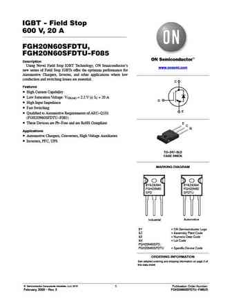
IGBT - Field Stop 600 V, 20 A FGH20N60SFDTU, FGH20N60SFDTU-F085 Description Using Novel Field Stop IGBT Technology, ON Semiconductor s www.onsemi.com new series of Field Stop IGBTs offer the optimum performance for Automotive Chargers, Inverter, and other applications where low conduction and switching losses are essential. C Features High Current Capability Low Saturati
hgtg20n60a4 hgtp20n60a4.pdf
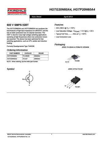
HGTG20N60A4, HGTP20N60A4 Data Sheet April 2013 File Number Features 600 V SMPS IGBT 40 A, 600 V @ TC = 110 C The HGTG20N60A4 and HGTP20N60A4 are combines the best features of high input impedance of a MOSFET and the Low Saturation Voltage VCE(sat) = 1.8 V @ IC = 20 A low on-state conduction loss of a bipolar transistor. This Typical Fall Time............55ns at TJ = 1

fcb20n60f.pdf

Is Now Part of To learn more about ON Semiconductor, please visit our website at www.onsemi.com Please note As part of the Fairchild Semiconductor integration, some of the Fairchild orderable part numbers will need to change in order to meet ON Semiconductor s system requirements. Since the ON Semiconductor product management systems do not have the ability to manage part nomenclatur
fcb20n60.pdf

Is Now Part of To learn more about ON Semiconductor, please visit our website at www.onsemi.com Please note As part of the Fairchild Semiconductor integration, some of the Fairchild orderable part numbers will need to change in order to meet ON Semiconductor s system requirements. Since the ON Semiconductor product management systems do not have the ability to manage part nomenclatur
apt20n60bc3.pdf
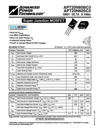
APT20N60BC3 APT20N60SC3 600V 20.7A 0.190 Super Junction MOSFET D3PAK TO-247 COOLMOS Power Semiconductors Ultra low RDS(ON) Low Miller Capacitance D Ultra Low Gate Charge, Qg Avalanche Energy Rated G TO-247 or Surface Mount D3PAK Package S MAXIMUM RATINGS All Ratings TC = 25 C unless otherwise specified. Symbol Parameter APT17N80BC3_S
fmw20n60s1hf.pdf
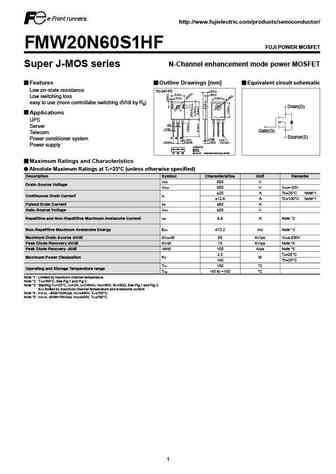
http //www.fujielectric.com/products/semiconductor/ FMW20N60S1HF FUJI POWER MOSFET Super J-MOS series N-Channel enhancement mode power MOSFET Features Outline Drawings [mm] Equivalent circuit schematic Low on-state resistance TO-247-P2 Low switching loss easy to use (more controllabe switching dV/dt by R ) g Drain(D) Applications UPS Server Gate(G) Telecom Source(S)
fmv20n60s1.pdf
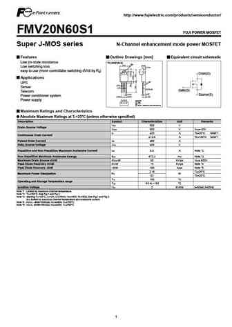
http //www.fujielectric.com/products/semiconductor/ FMV20N60S1 FUJI POWER MOSFET Super J-MOS series N-Channel enhancement mode power MOSFET Features Outline Drawings [mm] Equivalent circuit schematic Low on-state resistance TO-220F(SLS) Low switching loss easy to use (more controllabe switching dV/dt by R ) g Drain(D) Applications UPS Server Gate(G) Telecom Source(S) Power condi
fmp20n60s1.pdf
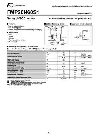
http //www.fujielectric.com/products/semiconductor/ FMP20N60S1 FUJI POWER MOSFET Super J-MOS series N-Channel enhancement mode power MOSFET Features Outline Drawings [mm] Equivalent circuit schematic Low on-state resistance 4.5 0.2 TO-220 10+0.5 0 1.3 0.2 Low switching loss easy to use (more controllabe switching dV/dt by R ) g Drain(D) Applications UPS 1.2 0.2 Server PRE-S
fmh20n60s1.pdf
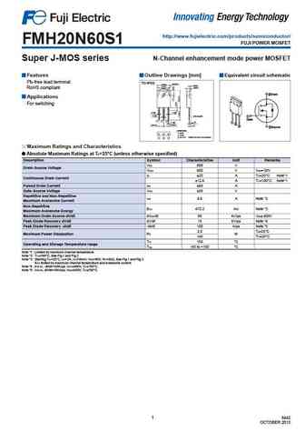
http //www.fujielectric.com/products/semiconductor/ FMH20N60S1 FUJI POWER MOSFET Super J-MOS series N-Channel enhancement mode power MOSFET Features Outline Drawings [mm] Equivalent circuit schematic Pb-free lead terminal TO-3P(Q) 3.2 0.1 15.5max 1.5 0.2 13 0.2 4.5 0.2 RoHS compliant 10 0.2 Drain Applications For switching +0.3 +0.3 1.6 -0.1 1.6 -0.1 +0.3 2.2 -0
hgtp20n60c3r.pdf
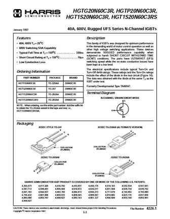
HGTG20N60C3R, HGTP20N60C3R, S E M I C O N D U C T O R HGT1S20N60C3R, HGT1S20N60C3RS 40A, 600V, Rugged UFS Series N-Channel IGBTs January 1997 Features Description 40A, 600V TJ = 25oC This family of IGBTs was designed for optimum performance in the demanding world of motor control operation as well as 600V Switching SOA Capability other high voltage switching applications. These
hgtg20n60c3r.pdf

HGTG20N60C3R, HGTP20N60C3R, S E M I C O N D U C T O R HGT1S20N60C3R, HGT1S20N60C3RS 40A, 600V, Rugged UFS Series N-Channel IGBTs January 1997 Features Description 40A, 600V TJ = 25oC This family of IGBTs was designed for optimum performance in the demanding world of motor control operation as well as 600V Switching SOA Capability other high voltage switching applications. These
kgf20n60pa.pdf
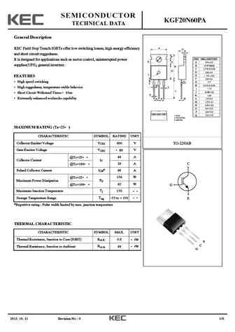
SEMICONDUCTOR KGF20N60PA TECHNICAL DATA General Description KEC Field Stop Trench IGBTs offer low switching losses, high energy efficiency and short circuit ruggedness. It is designed for applications such as motor control, uninterrupted power supplies(UPS), general inverters. FEATURES High speed switching High ruggedness, temperature stable behavior Short Circuit Withstand Ti
kgt20n60kda.pdf
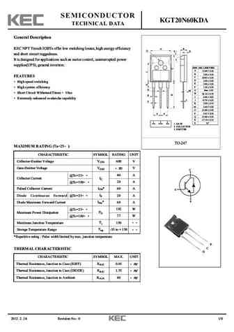
SEMICONDUCTOR KGT20N60KDA TECHNICAL DATA General Description KEC NPT Trench IGBTs offer low switching losses, high energy efficiency B A O S K and short circuit ruggedness. It is designed for applications such as motor control, uninterrupted power supplies(UPS), general inverters. DIM MILLIMETERS _ + A 15.90 0.30 _ B 5.00 + 0.20 FEATURES _ C 20.85 + 0.30 _ D 3.00 + 0.20
kgf20n60kda.pdf
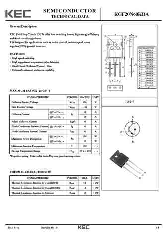
SEMICONDUCTOR KGF20N60KDA TECHNICAL DATA General Description KEC Field Stop Trench IGBTs offer low switching losses, high energy efficiency and short circuit ruggedness. It is designed for applications such as motor control, uninterrupted power supplies(UPS), general inverters. FEATURES High speed switching High ruggedness, temperature stable behavior Short Circuit Withstand T
20n60a msafx20n60a.pdf
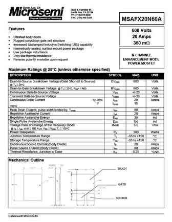
2830 S. Fairview St. Santa Ana, CA 92704 PH (714) 979-8220 FAX (714) 966-5256 MSAFX20N60A Features 600 Volts Ultrafast body diode 20 Amps Rugged polysilicon gate cell structure 350 m Increased Unclamped Inductive Switching (UIS) capability Hermetically sealed, surface mount power package Low package inductance N-CHANNEL Very low thermal resistance
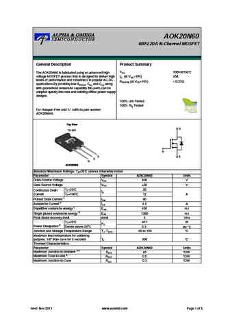
aok20n60.pdf

AOK20N60 600V,20A N-Channel MOSFET General Description Product Summary VDS 700V@150 The AOK20N60 is fabricated using an advanced high voltage MOSFET process that is designed to deliver high ID (at VGS=10V) 20A levels of performance and robustness in popular AC-DC RDS(ON) (at VGS=10V)
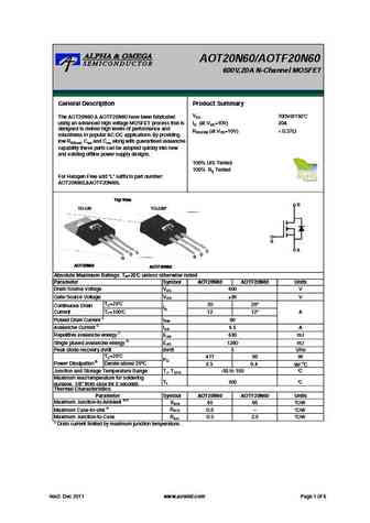
aotf20n60.pdf

AOT20N60/AOTF20N60 600V,20A N-Channel MOSFET General Description Product Summary VDS 700V@150 The AOT20N60 & AOTF20N60 have been fabricated using an advanced high voltage MOSFET process that is ID (at VGS=10V) 20A designed to deliver high levels of performance and RDS(ON) (at VGS=10V)
aot20n60 aotf20n60.pdf

AOT20N60/AOTF20N60 600V,20A N-Channel MOSFET General Description Product Summary VDS 700V@150 The AOT20N60 & AOTF20N60 have been fabricated using an advanced high voltage MOSFET process that is ID (at VGS=10V) 20A designed to deliver high levels of performance and RDS(ON) (at VGS=10V)
aok20n60l.pdf
AOK20N60 600V,20A N-Channel MOSFET General Description Product Summary VDS 700V@150 The AOK20N60 is fabricated using an advanced high voltage MOSFET process that is designed to deliver high ID (at VGS=10V) 20A levels of performance and robustness in popular AC-DC RDS(ON) (at VGS=10V)
aot20n60.pdf
AOT20N60/AOTF20N60 600V,20A N-Channel MOSFET General Description Product Summary VDS 700V@150 The AOT20N60 & AOTF20N60 have been fabricated using an advanced high voltage MOSFET process that is ID (at VGS=10V) 20A designed to deliver high levels of performance and RDS(ON) (at VGS=10V)
aot20n60l.pdf

AOT20N60/AOTF20N60 600V,20A N-Channel MOSFET General Description Product Summary VDS 700V@150 The AOT20N60 & AOTF20N60 have been fabricated using an advanced high voltage MOSFET process that is ID (at VGS=10V) 20A designed to deliver high levels of performance and RDS(ON) (at VGS=10V)

mp20n60ei.pdf
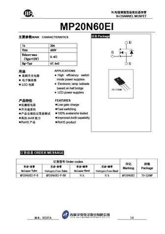
N R N-CHANNEL MOSFET MP20N60EI Package MAIN CHARACTERISTICS ID 20A VDSS 600V Rdson-max 0.4 Vgs=10V Qg-Typ 67.6nC APPLICATIONS High efficiency switch mode power supplies Electronic lamp ballasts LED based on half bridge LE
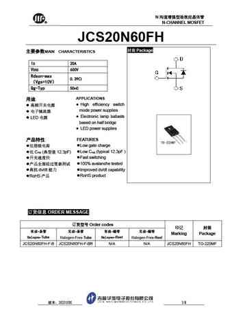
jcs20n60fh.pdf
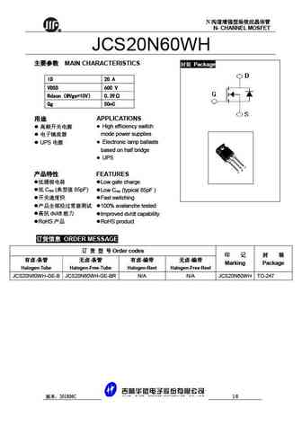
N R N-CHANNEL MOSFET JCS20N60FH Package MAIN CHARACTERISTICS ID 20A VDSS 600V Rdson-max 0.39 Vgs=10V Qg-Typ 50nC APPLICATIONS High efficiency switch mode power supplies Electronic lamp ballasts LED based on half bridge LE
ssf20n60h.pdf
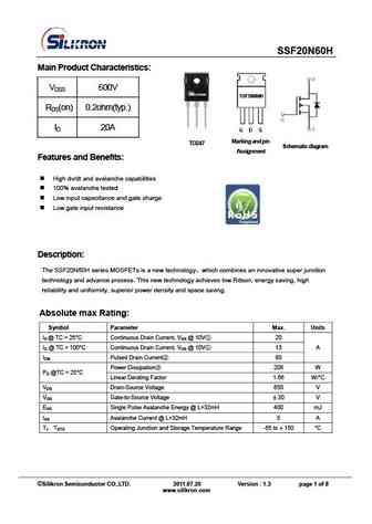
SSF20N60H Main Product Characteristics VDSS 600V RDS(on) 0.2ohm(typ.) ID 20A Marking a nd p in TO247 Sche ma ti c di agr a m Assignment Features and Benefits High dv/dt and avalanche capabilities 100% avalanche tested Low input capacitance and gate charge Low gate input resistance Description The SSF20N60H series MOSFETs is a new technology w
brf20n60.pdf
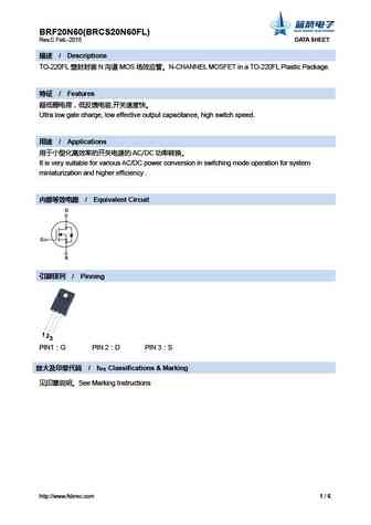
BRF20N60(BRCS20N60FL) Rev.C Feb.-2015 DATA SHEET / Descriptions TO-220FL N MOS N-CHANNEL MOSFET in a TO-220FL Plastic Package. / Features , Ultra low gate charge, low effective output capacitance, high switch speed. / Applications
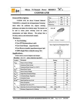
cs20n60 anh.pdf

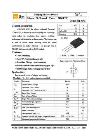
Silicon N-Channel Power MOSFET R CS20N60 ANH VDSS 600 V General Description ID 20 A CS20N60 ANH, the silicon N-channel Enhanced PD(TC=25 ) 250 W VDMOSFETs, is obtained by the self-aligned planar Technology RDS(ON)Typ 0.36 which reduce the conduction loss, improve switching performance and enhance the avalanche energy. The transistor can be used in various po
cs20n60 a8h.pdf
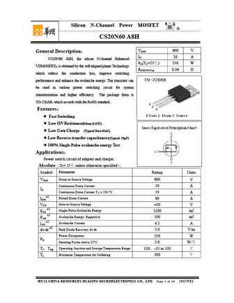
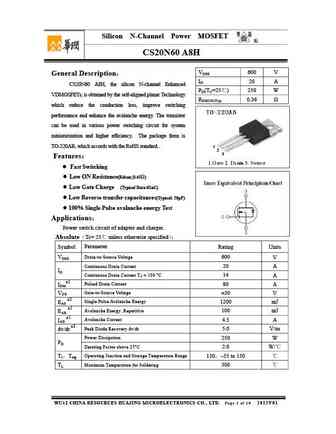
Silicon N-Channel Power MOSFET R CS20N60 A8H VDSS 600 V General Description ID 20 A CS20N60 A8H, the silicon N-channel Enhanced PD(TC=25 ) 250 W VDMOSFETs, is obtained by the self-aligned planar Technology RDS(ON)Typ 0.36 which reduce the conduction loss, improve switching performance and enhance the avalanche energy. The transistor can be used in various po
cs20n60f a9h.pdf
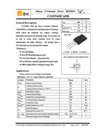
Silicon N-Channel Power MOSFET R CS20N60F A9H VDSS 600 V General Description ID 20 A CS20N60F A9H, the silicon N-channel Enhanced PD(TC=25 ) 85 W VDMOSFETs, is obtained by the self-aligned planar Technology RDS(ON)Typ 0.36 which reduce the conduction loss, improve switching performance and enhance the avalanche energy. The transistor can be used in various
cs20n60.pdf
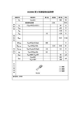
CS20N60 N PD TC=25 300 W 2.38 W/ ID VGS=10V,TC=25 20 A VGS 20 V Tjm +150 Tstg -55 +150 RthJC 0.42 /W BVDSS VGS=0V,ID=0.25mA 600 V RDS on VGS=10V,ID=10A 0.32 0.46 VGS th VDS=VGS,ID=0.25m
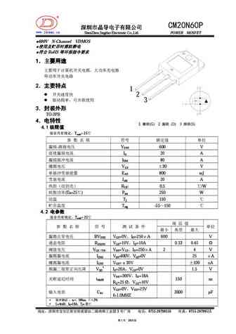
cm20n60.pdf
R CM20N60 www.jdsemi.cn ShenZhen Jingdao Electronic Co.,Ltd. POWER MOSFET 600V N-Channel VDMOS RoHS 1 2 3
f20n60.pdf
F20N60 20A 600V N-channel Enhancement Mode Power MOSFET 1 Description These N-channel enhanced vdmosfets, is obtained by the self-aligned V DSS = 600V planar technology which reduce the conduction loss, improve switching I = 20.0A D performance and enhance the avalanche energy. Which accords with the RoHS standard. TO-220F provides insulation voltage rated at 2000V R DS(on) TYP)
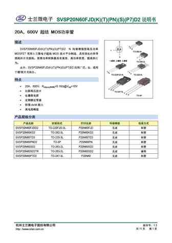
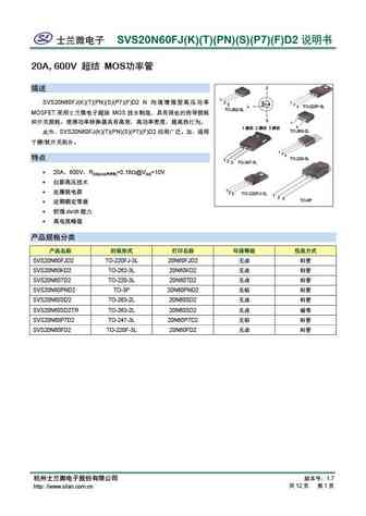
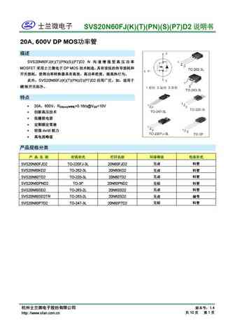
svsp20n60fjdd2 svsp20n60kd2 svsp20n60td2 svsp20n60pnd2 svsp20n60sd2 svsp20n60sd2tr svsp20n60p7d2.pdf
svs20n60fjd2 svs20n60kd2 svs20n60td2 svs20n60pnd2 svs20n60sd2 svs20n60sd2tr svs20n60p7d2 svs20n60fd2.pdf
svs20n60fjd2 svs20n60kd2 svs20n60td2 svs20n60pnd2 svs20n60sd2 svs20n60sd2tr svs20n60p7d2.pdf
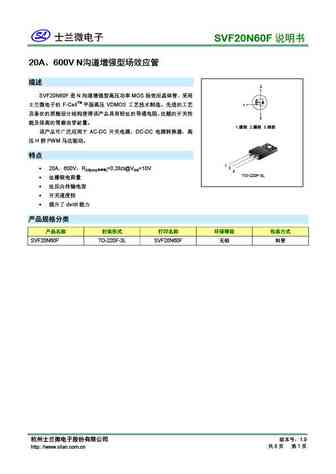
svf20n60f svf20n60pn.pdf
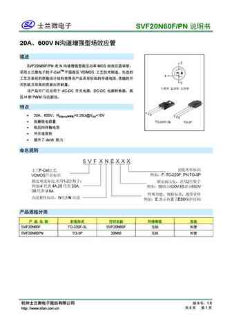
SVF20N60F/PN 20A 600V N SVF20N60F/PN N MOS F-CellTM VDMOS
msw20n60.pdf
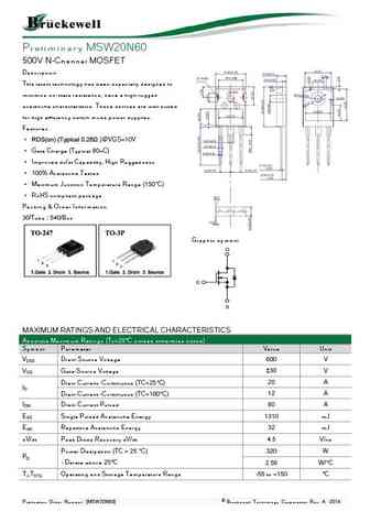
Preliminary MSW20N60 500V N-Channel MOSFET Description This latest technology has been especially designed to minimize on-state resistance, have a high rugged avalanche characteristics. These devices are well suited for high efficiency switch mode power supplies. Features RDS(on) (Typical 0.26 )@VGS=10V Gate Charge (Typical 80nC) Improved dv/dt Capability, High
wff20n60s.pdf
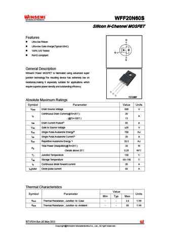
WFF20N60S WFF20N60S WFF20N60S WFF20N60S Silicon N-Channel MOSFET Silicon N-Channel MOSFET Silicon N-Channel MOSFET Silicon N-Channel MOSFET Features Ultra low Rdson Ultra-low Gate charge(Typical 68nC) 100% UIS Tested RoHS compliant General Description Winsemi Power MOSFET is fabricated using advanced super junction technology.The resulting device has extremely low
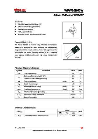
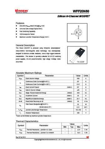
wfw20n60w.pdf
WFW20N60W WFW20N60W WFW20N60W WFW20N60W Silicon N-Channel MOSFET Silicon N-Channel MOSFET Silicon N-Channel MOSFET Silicon N-Channel MOSFET Features 20A,600V,R (Max0.39 )@V =10V DS(on) GS Ultra-low Gate charge(Typical 150nC) Fast Switching Capability 100%Avalanche Tested Maximum Junction Temperature Range(150 ) General Description This Power MOSFET is pro
wff20n60.pdf
WFF20N60 WFF20N60 WFF20N60 WFF20N60 Silicon N-Channel MOSFET Silicon N-Channel MOSFET Silicon N-Channel MOSFET Silicon N-Channel MOSFET Features 20A,600V,R (Max0.39 )@V =10V DS(on) GS Ultra-low Gate charge(Typical 50nC) Fast Switching Capability 100%Avalanche Tested Maximum Junction Temperature Range(150 ) General Description This Power MOSFET is produced
bl20n60-p bl20n60-a bl20n60-w bl20n60-f.pdf
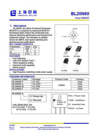
BL20N60 Power MOSFET 1 Description Step-Down Converter BL20N60, the silicon N-channel Enhanced , MOSFETs, is obtained by advanced MOSFET technology which reduce the conduction loss, improve switching performance and enhance the avalanche energy. The transistor is suitable device for SMPS, high speed switching and general purpose applications. KEY CHARACTERISTICS Pa
cs20n60fa9h.pdf
CS20N60FA9H 600V Silicon N-Channel Power MOSFET Features Outline Fast switching. TO-220F ESD improved capability. 0.189(4.80) 0.173(4.40) Low gate charge. 0.409(10.40) 0.378(9.60) 0.114(2.90) Low reverse transfer capacitances. 0.098(2.50) 100% single pulse avalanche energy test. 0.638(16.20) 0.606(15.40) Marking code Mechanical data G D S Ep
jfhm20n60e.pdf
JFHM20N60E 600V N-Channel MOSFET General Description This Power MOSFET is produced using advanced planar stripe DMOS technology. This advanced technology has been especially tailored to minimize on-state resistance, provide superior switching performance, and withstand high energy pulse in the avalanche and commutation mode. These devices are well suited for high efficiency
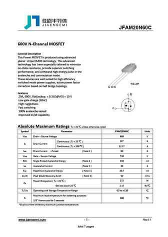
jfam20n60e.pdf
JFAM20N60E 600V N-Channel MOSFET General Description This Power MOSFET is produced using advanced planar stripe DMOS technology. This advanced technology has been especially tailored to minimize on-state resistance, provide superior switching performance, and withstand high energy pulse in the avalanche and commutation mode. These devices are well suited for high efficiency
jffm20n60c.pdf

JFFM20N60C 600V N-Channel MOSFET General Description This Power MOSFET is produced using advanced planar stripe DMOS technology. This advanced technology has been especially tailored to minimize on-state resistance, provide superior switching performance, and withstand high energy pulse in the avalanche and commutation mode. These devices are well suited for high efficiency
jfhm20n60c.pdf
JFHM20N60C 600V N-Channel MOSFET General Description This Power MOSFET is produced using advanced planar stripe DMOS technology. This advanced technology has been especially tailored to minimize on-state resistance, provide superior switching performance, and withstand high energy pulse in the avalanche and commutation mode. These devices are well suited for high efficiency
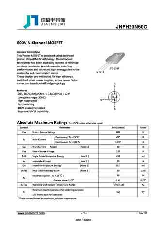
jnfh20n60c.pdf
JNFH20N60C 600V N-Channel MOSFET General Description This Power MOSFET is produced using advanced planar stripe DMOS technology. This advanced technology has been especially tailored to minimize on-state resistance, provide superior switching performance, and withstand high energy pulse in the avalanche and commutation mode. These devices are well suited for high efficiency
jnfh20n60e.pdf
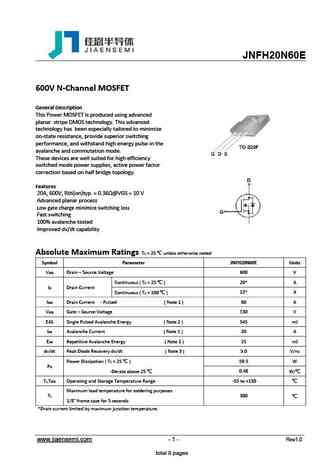
JNFH20N60E 600V N-Channel MOSFET General Description This Power MOSFET is produced using advanced planar stripe DMOS technology. This advanced technology has been especially tailored to minimize on-state resistance, provide superior switching performance, and withstand high energy pulse in the avalanche and commutation mode. These devices are well suited for high efficiency
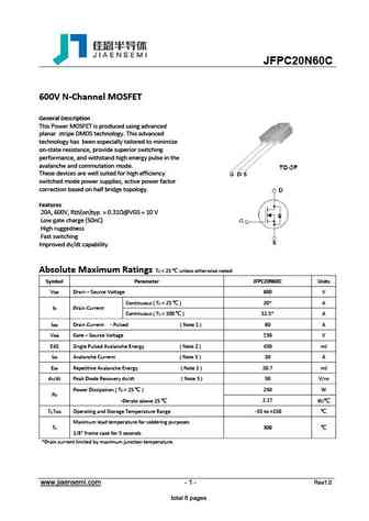
jfpc20n60c.pdf
JFPC20N60C 600V N-Channel MOSFET General Description This Power MOSFET is produced using advanced planar stripe DMOS technology. This advanced technology has been especially tailored to minimize on-state resistance, provide superior switching performance, and withstand high energy pulse in the avalanche and commutation mode. These devices are well suited for high efficiency
jfam20n60d.pdf

JFAM20N60D 600V N-Channel MOSFET General Description This Power MOSFET is produced using advanced planar stripe DMOS technology. This advanced technology has been especially tailored to minimize on-state resistance, provide superior switching performance, and withstand high energy pulse in the avalanche and commutation mode. These devices are well suited for high efficiency
jfam20n60c.pdf
JFAM20N60C 600V N-Channel MOSFET General Description This Power MOSFET is produced using advanced planar stripe DMOS technology. This advanced technology has been especially tailored to minimize on-state resistance, provide superior switching performance, and withstand high energy pulse in the avalanche and commutation mode. These devices are well suited for high efficiency
ncep020n60agu.pdf
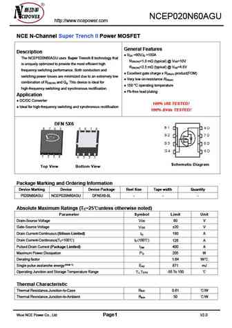
NCEP020N60AGU http //www.ncepower.com NCE N-Channel Super Trench II Power MOSFET General Features Description V =60V,I =180A DS D The NCEP020N60AGU uses Super Trench II technology that R =1.8 m (typical) @ V =10V DS(ON) GS is uniquely optimized to provide the most efficient high R =2.5 m (typical) @ V =4.5V DS(ON) GS frequency switching performance. Both conduction and
nceap020n60gu.pdf
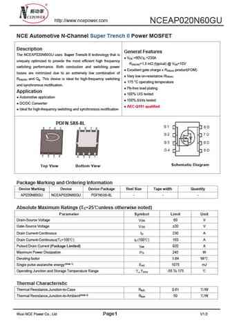
http //www.ncepower.com NCEAP020N60GU NCE Automotive N-Channel Super Trench II Power MOSFET Description General Features The NCEAP020N60GU uses Super Trench II technology that is V =60V,I =230A DS D uniquely optimized to provide the most efficient high frequency R =1.8 m (typical) @ V =10V DS(ON) GS switching performance. Both conduction and switching power Excellent gate
ncep020n60gu.pdf
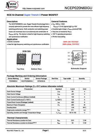
http //www.ncepower.com NCEP020N60GU NCE N-Channel Super Trench II Power MOSFET Description General Features The NCEP020N60GU uses Super Trench II technology that is V =60V,I =180A DS D uniquely optimized to provide the most efficient high frequency R =1.8 m (typical) @ V =10V DS(ON) GS switching performance. Both conduction and switching power Excellent gate charge x R product
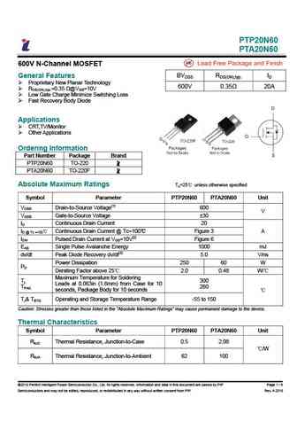
ptp20n60a pta20n60a.pdf
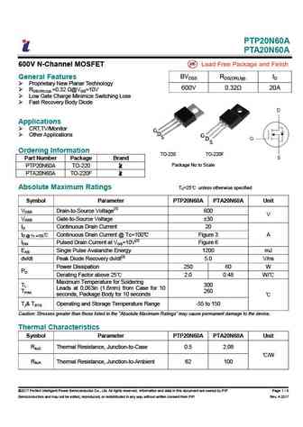
PTP20N60A PTA20N60A 600V N-Channel MOSFET General Features BVDSS RDS(ON),typ. ID Proprietary New Planar Technology 600V 0.32 20A RDS(ON),typ.=0.32 @VGS=10V Low Gate Charge Minimize Switching Loss Fast Recovery Body Diode Applications CRT,TV/Monitor G D S Other Applications G D S Ordering Information TO-220 TO-220F Part Number Pa
ptp20n60 pta20n60.pdf
PTP20N60 PTA20N60 600V N-Channel MOSFET General Features BVDSS RDS(ON),typ. ID Proprietary New Planar Technology 600V 0.35 20A RDS(ON),typ.=0.35 @VGS=10V Low Gate Charge Minimize Switching Loss Fast Recovery Body Diode Applications CRT,TV/Monitor Other Applications Ordering Information Part Number Package Brand PTP20N60 TO-220 PTA20N60 TO-2
ps20n600a.pdf

PS20N600A 600V Single Channel NMOSEFT Revision 1.0 Update Date Jan. 2012 ProsPower Microelectronics Co., Ltd PS20N600A 600V Single Channel NMOSFET 2. Applications 1. General Description Power factor correction (PFC) The PS20N600A uses advanced high voltage Switched mode power supplies (SMPS) technology and design to provide excellent Rds(on) Uninterruptible P
swf20n60k.pdf
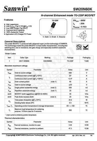
SW20N60K N-channel Enhanced mode TO-220F MOSFET Features TO-220F BVDSS 600V ID 20A High ruggedness Low RDS(ON) (Typ 0.15 )@VGS=10V RDS(ON) 0.15 Low Gate Charge (Typ 60nC) Improved dv/dt Capability 2 1 100% Avalanche Tested 2 3 Application LED,Charger,PC Power 1 1. Gate 2. Drain 3. Source 3 General Description This power
sw20n60k swf20n60k.pdf

SW20N60K N-channel Enhanced mode TO-220F MOSFET Features TO-220F BVDSS 600V ID 20A High ruggedness Low RDS(ON) (Typ 0.15 )@VGS=10V RDS(ON) 0.15 Low Gate Charge (Typ 60nC) Improved dv/dt Capability 2 1 100% Avalanche Tested 2 3 Application LED,Charge,PC Power 1 1. Gate 2. Drain 3. Source 3 General Description This power
hia20n60bp.pdf
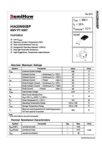
Dec 2013 VCES = 600 V IC = 20 A HIA20N60BP VCE(sat) typ = 2.2 V 600V PT IGBT TO-247 FEATURES Low VCE(sat) Maximum Junction Temperature 150 G C E Short Circuit Withstand Time 5 Designed for Operation Between 1-20KHz Very tight Parameter Distribution High Ruggedness, Temperature stable behavior Absolute Maximum Ratings Symbol Parameter Value Units VCES Collector-
hih20n60bp.pdf
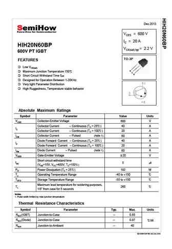
Dec 2013 VCES = 600 V IC = 20 A HIH20N60BP VCE(sat) typ = 2.2 V 600V PT IGBT TO-3P FEATURES Low VCE(sat) G Maximum Junction Temperature 150 C E Short Circuit Withstand Time 5 Designed for Operation Between 1-20KHz Very tight Parameter Distribution High Ruggedness, Temperature stable behavior Absolute Maximum Ratings Symbol Parameter Value Units VCES Collector-E
tgpf20n60fdr.pdf

TGPF20N60FDR Field Stop Trench IGBT Features 600V Field Stop Trench IGBT Technology High Speed Switching Low Conduction Loss Positive Temperature Coefficient Easy Parallel Operation Short Circuit Withstanding Time 5 s 175 Operating Temperature RoHS Compliant JEDEC Qualification Applications Motor Drive, Air Conditioner, Inverter, Solar Devic
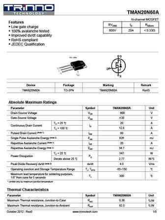
tman20n60a.pdf
TMAN20N60A N-channel MOSFET Features BVDSS ID RDS(on) Low gate charge 600V 20A
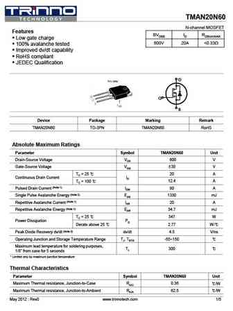
tman20n60.pdf
TMAN20N60 N-channel MOSFET Features BVDSS ID RDS(on)MAX Low gate charge 600V 20A
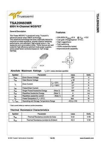
tsa20n60mr.pdf
TSA20N60MR 600V N-Channel MOSFET General Description Features This Power MOSFET is produced using Truesemi s 20A,600V,RDS(on)=0.4 @ VGS =10V advanced planar stripe DMOS technology. This advanced technology has been especially tailored to Low gate charge(typical 57nC) minimize on-state resistance, provide superior switching High ruggedness performance, and withs
tsf20n60mr.pdf

TSF20N60MR 600V N-Channel MOSFET General Description Features This Power MOSFET is produced using Truesemi s 20A,600V,RDS(on)=0.4 @ VGS =10V advanced planar stripe DMOS technology. This advanced technology has been especially tailored to Low gate charge(typical 57nC) minimize on-state resistance, provide superior switching High ruggedness performance, and wi
cs20n60anh.pdf
Silicon N-Channel Power MOSFET R CS20N60 ANH VDSS 600 V General Description ID 20 A CS20N60 ANH, the silicon N-channel Enhanced PD(TC=25 ) 250 W VDMOSFETs, is obtained by the self-aligned planar Technology RDS(ON)Typ 0.36 which reduce the conduction loss, improve switching performance and enhance the avalanche energy. The transistor can be used in various po
cs20n60fa9h.pdf
Huajing Discrete Devices R Silicon N-Channel Power MOSFET CS20N60F A9H VDSS 600 V General Description ID 20 A CS20N60F A9H, the silicon N-channel Enhanced PD(TC=25 ) 85 W VDMOSFETs, is obtained by the self-aligned planar Technology RDS(ON)Typ 0.36 which reduce the conduction loss, improve switching performance and enhance the avalanche energy. The transisto
cs20n60a8h.pdf
Silicon N-Channel Power MOSFET R CS20N60 A8H VDSS 600 V General Description ID 20 A CS20N60 A8H, the silicon N-channel Enhanced PD(TC=25 ) 250 W VDMOSFETs, is obtained by the self-aligned planar Technology RDS(ON)Typ 0.36 which reduce the conduction loss, improve switching performance and enhance the avalanche energy. The transistor can be used in various po
cs20n60f cs20n60p.pdf
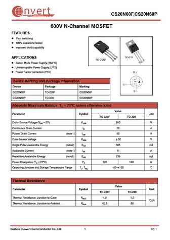
nvert CS20N60F,CS20N60P Suzhou Convert Semiconductor Co ., Ltd. 600V N-Channel MOSFET FEATURES Fast switching 100% avalanche tested Improved dv/dt capability APPLICATIONS Switch Mode Power Supply (SMPS) Uninterruptible Power Supply (UPS) Power Factor Correction (PFC) Device Marking and Package Information Device Package Marking CS20N60F TO-220F CS20N60F CS
cs20n60f cs20n60p cs20n60w cs20n60v.pdf
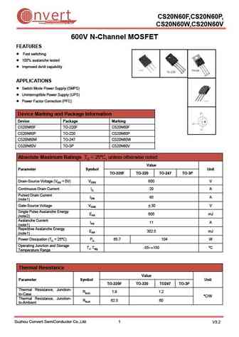
CS20N60F,CS20N60P, nvert Suzhou Convert Semiconductor Co ., Ltd. CS20N60W,CS20N60V 600V N-Channel MOSFET FEATURES Fast switching 100% avalanche tested Improved dv/dt capability APPLICATIONS Switch Mode Power Supply (SMPS) Uninterruptible Power Supply (UPS) Power Factor Correction (PFC) Device Marking and Package Information Device Package Marking CS20N60F
csfr20n60f.pdf
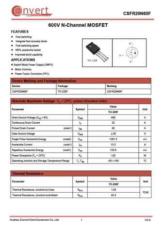
nvert CSFR20N60F Suzhou Convert Semiconductor Co ., Ltd. 600V N-Channel MOSFET FEATURES Fast switching Integrate fast recovery diode Fast switching speed 100% avalanche tested Improved dv/dt capability APPLICATIONS Switch Mode Power Supply (SMPS) Motor Controls Power Factor Correction (PFC) Device Marking and Package Information Device Package Marki
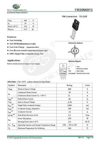
fir20n60fg.pdf
FIR20N60FG N-Channel Power MOSFET PIN Connection TO-220F VDSS 600 V ID 20 A PD(TC=25 ) 250 W RDS(ON) 0.35 G Features D S Fast Switching g Schematic dia ram Low ON Resistance(Rdso D Low Gate Charge (Typical Data 70nC) Low Reverse transfer capacitances(Typical 32pF) G 100% Single Pulse avalanche energy Test S Applications Marking Diagr
ha20n60.pdf
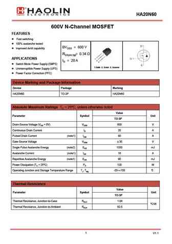
HA20N60 600V N-Channel MOSFET FEATURES Fast switching 100% avalanche tested BVDSS = 600 V Improved dv/dt capability RDS(on) typ = 0.34 1 APPLICATIONS 2 ID = 20 A 3 Switch Mode Power Supply (SMPS) 1.Gate 2. Drain 3. Source Uninterruptible Power Supply (UPS) Power Factor Correction (PFC) Device Marking and Package Information Device Package Marking
hf20n60 hp20n60.pdf
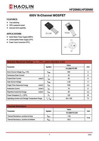
HF20N60,HP20N60 600V N-Channel MOSFET FEATURES Fast switching 100% avalanche tested Improved dv/dt capability APPLICATIONS Switch Mode Power Supply (SMPS) Uninterruptible Power Supply (UPS) Power Factor Correction (PFC) Absolute Maximum Ratings TC = 25 unless otherwise noted C, Value Parameter Symbol Unit TO-220 TO-220F/ Drain-Source Voltage (VGS = 0V)
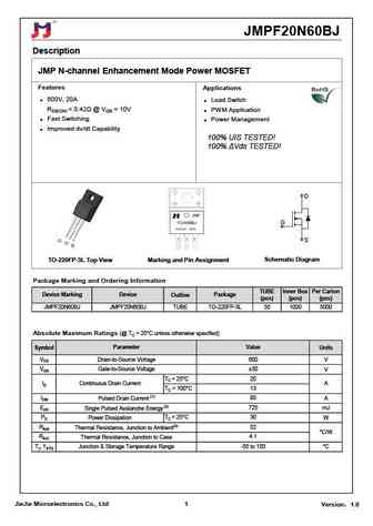
jmpf20n60bj.pdf
JMPF20N60BJ Description JMP N-channel Enhancement Mode Power MOSFET Features Applications 600V, 20A Load Switch RDS(ON)
jmpc20n60bj.pdf
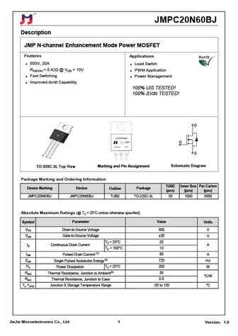
JMPC20N60BJ Description JMP N-channel Enhancement Mode Power MOSFET Features Applications 600V, 20A Load Switch RDS(ON)
lnc20n60 lnd20n60 lnb20n60.pdf
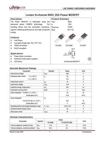
LNC20N60/ LND20N60/LNB20N60 Lonten N-channel 600V, 20A Power MOSFET Description Product Summary The Power MOSFET is fabricated using the V 600V DSS advanced planer VDMOS technology. The I 20A D resulting device has low conduction resistance, R 0.45 DS(on),max superior switching performance and high avalanche Q 63.7 nC g,typ energy. Features Low R DS(on) Low gate charge
sig20n60p1a.pdf
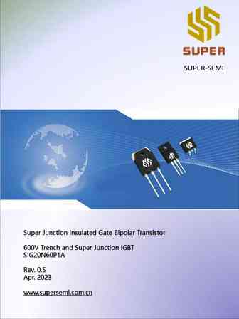
SUPER-SEMI Super Junction Insulated Gate Bipolar Transistor 600V Trench and Super Junction IGBT SIG20N60P1A Rev. 0.5 Apr. 2023 www.supersemi.com.cn SIG20N60P1A 600V Trench and Super Junction IGBT General Description Super-Semi Trench and Super Junction IGBTs, VCE 600 V designed according to the superjunction (SJ) IC 20 A principle. The SJ-IGBT series provides low VCE(sat) I
ssf20n60s ssp20n60s ssb20n60s.pdf
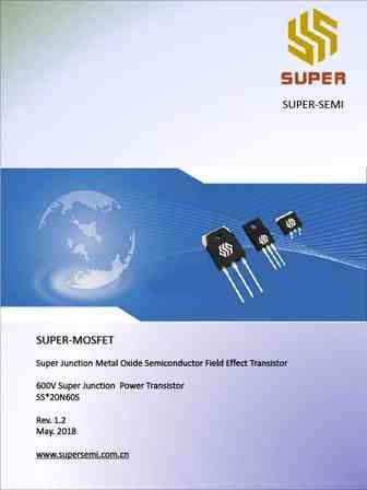
SUPER-SEMI SUPER-MOSFET Super Junction Metal Oxide Semiconductor Field Effect Transistor 600V Super Junction Power Transistor SS*20N60S Rev. 1.2 May. 2018 www.supersemi.com.cn September, 2013 SJ-FET SSF20N60S/SSP20N60S/SSB20N60S 600V N-Channel MOSFET Description Features SJ-FET is new generation of high voltage MOSFET family that Multi-Epi process SJ-FET is
sig20n60f.pdf

SUPER-SEMI Super Junction Insulated Gate Bipolar Transistor 600V Trench and Super Junction IGBT SIG20N60F Rev. 0.5 Apr. 2023 www.supersemi.com.cn SIG20N60F 600V Trench and Super Junction IGBT General Description Super-Semi Trench and Super Junction IGBTs, VCE 600 V designed according to the superjunction (SJ) IC 20 A principle. The SJ-IGBT series provides low VCE(sat) IC=20
sig20n60f sig20n60p.pdf
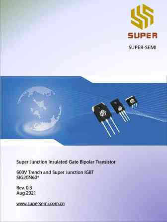
SUPER-SEMI Super Junction Insulated Gate Bipolar Transistor 600V Trench and Super Junction IGBT SIG20N60* Rev. 0.3 Aug.2021 www.supersemi.com.cn SIG20N60F/SIG20N60P 600V Trench and Super Junction IGBT General Description Super-Semi Trench and Super Junction IGBTs, VCE 600 V designed according to the superjunction (SJ) IC 20 A principle. The SJ-IGBT series provides low VCE(sat
ssw20n60s ssa20n60s.pdf

SUPER-SEMI SUPER-MOSFET Super Junction Metal Oxide Semiconductor Field Effect Transistor 600V Super Junction Power Transistor SS*20N60S Rev. 1.2 May. 2018 www.supersemi.com.cn September, 2013 SJ-FET SSW20N60S/SSA20N60S 600V N-Channel MOSFET Description Features SJ-FET is new generation of high voltage MOSFET family that Multi-Epi process SJ-FET is utilizing
dgw20n60ctl.pdf
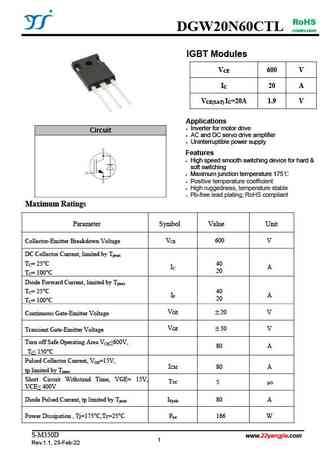
RoHS DGW20N60CTL COMPLIANT IGBT Modules IGBT Descrete V 600 V CE I 20 A C V I =20A 1.9 V CE(SAT) C Applications Inverter for motor drive Circuit AC and DC servo drive amplifier Uninterruptible power supply Features High speed smooth switching device for hard & soft switching Maximum junction temperature 175 Positive temperature
hm20n60a.pdf
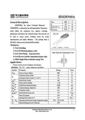
HM20N60A VDSS 600 V General Description ID 20 A HM20N60A, the silicon N-channel Enhanced PD(TC=25 ) 250 W VDMOSFETs, is obtained by the self-aligned planar Technology RDS(ON)Typ 0.36 which reduce the conduction loss, improve switching performance and enhance the avalanche energy. The transistor can be used in various power switching circuit for system miniaturiza
hm20n60.pdf
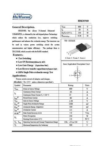
20N60 VDSS 600 V General Description ID 20 A HM20N60, the silicon N-channel Enhanced PD(TC=25 ) 250 W VDMOSFETs, is obtained by the self-aligned planar Technology RDS(ON)Typ 0.36 which reduce the conduction loss, improve switching performance and enhance the avalanche energy. The transistor can be used in various power switching circuit for system miniaturizati
hm20n60f.pdf
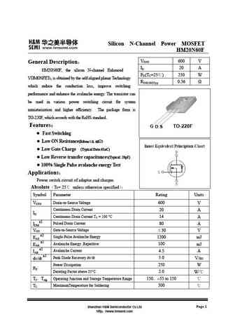
Silicon N-Channel Power MOSFET HM20N60F VDSS 600 V General Description ID 20 A HM20N60F, the silicon N-channel Enhanced PD(TC=25 ) 250 W VDMOSFETs, is obtained by the self-aligned planar Technology RDS(ON)Typ 0.36 which reduce the conduction loss, improve switching performance and enhance the avalanche energy. The transistor can be used in various power switching
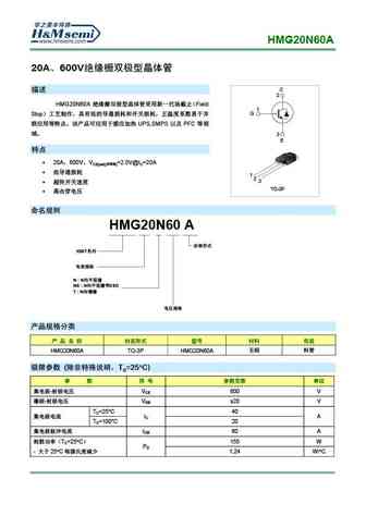
md20n60.pdf
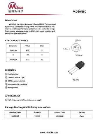
Description MD20N60,the silicon N-channel Enhanced MOSFETs,is obtained by advanced MOSFET technology which reduce the conduction loss improve switching performance and enhance the avalanche energy. The transistor is suitable device for SMPS, high speed switching and general purpose applications. KEY CHARACTERISTICS Parameter Value Unit VDS@Tj.max 600 V ID 20 A RDS(ON).TyP 0.39
ixfm20n60.pdf
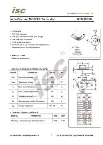
Isc N-Channel MOSFET Transistor IXFM20N60 FEATURES With To-3 package Low input capacitance and gate charge Low gate input resistance 100% avalanche tested Minimum Lot-to-Lot variations for robust device performance and reliable operation APPLICATIONS Switching applications ABSOLUTE MAXIMUM RATINGS(T =25 ) a SYMBOL PARAMETER VALUE UNIT V Drain-Source Voltage 600
spa20n60c3.pdf
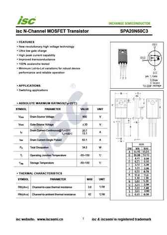
INCHANGE Semiconductor isc N-Channel MOSFET Transistor SPA20N60C3 FEATURES New revolutionary high voltage technology Ultra low gate charge High peak current capability Improved transconductance 100% avalanche tested Minimum Lot-to-Lot variations for robust device performance and reliable operation APPLICATIONS Switching applications ABSOLUTE MAXIMUM RATINGS(T =25
spp20n60c3.pdf
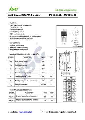
isc N-Channel MOSFET Transistor SPP20N60C3 ISPP20N60C3 FEATURES Static drain-source on-resistance RDS(on) 0.19 Enhancement mode Fast Switching Speed 100% avalanche tested Minimum Lot-to-Lot variations for robust device performance and reliable operation DESCRIPTION Ultra low gate charge High peak current capability Improved transconductance ABSOLUTE M
spa20n60cfd.pdf
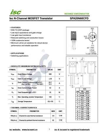
INCHANGE Semiconductor Isc N-Channel MOSFET Transistor SPA20N60CFD FEATURES With TO-220F package Low input capacitance and gate charge Low gate input resistance Reduced switching and conduction losses 100% avalanche tested Minimum Lot-to-Lot variations for robust device performance and reliable operation APPLICATIONS Switching applications ABSOLUTE MAXIMUM RATING
spb20n60s5.pdf
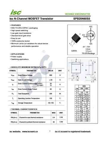
INCHANGE Semiconductor isc N-Channel MOSFET Transistor SPB20N60S5 FEATURES With TO-263( D2PAK ) packaging High speed switching Low gate input resistance Standard level gate drive Easy to use 100% avalanche tested Minimum Lot-to-Lot variations for robust device performance and reliable operation APPLICATIONS Power supply Switching applications ABSOLUTE MAXIM
fmv20n60s1.pdf
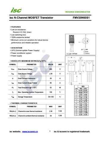
isc N-Channel MOSFET Transistor FMV20N60S1 FEATURES Low on-resistance RDS(on) 0.19 (max) Low switching loss 100% avalanche tested Minimum Lot-to-Lot variations for robust device performance and reliable operation DESCRITION UPS (Uninterruptible Power Supply) Power conditioner system Power supply ABSOLUTE MAXIMUM RATINGS(T =25 ) a SYMBOL PARAMETER VALU
fmp20n60s1.pdf
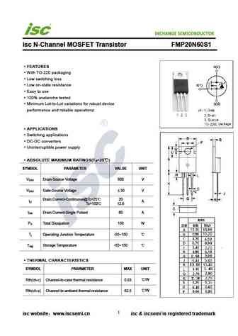
INCHANGE Semiconductor isc N-Channel MOSFET Transistor FMP20N60S1 FEATURES With TO-220 packaging Low switching loss Low on-state resistance Easy to use 100% avalanche tested Minimum Lot-to-Lot variations for robust device performance and reliable operationz APPLICATIONS Switching applications DC-DC converters Uninterruptible power supply ABSOLUTE MAXIMUM RA
aotf20n60.pdf
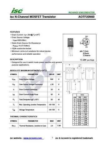
isc N-Channel MOSFET Transistor AOTF20N60 FEATURES Drain Current I = 20A@ T =25 D C Drain Source Voltage- V =600V(Min) DSS Static Drain-Source On-Resistance R =0.37 (Max) DS(on) 100% avalanche tested Minimum Lot-to-Lot variations for robust device performance and reliable operation DESCRIPTION Designed for use in switch mode power supplies and general purpo
spp20n60s5.pdf
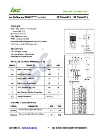
isc N-Channel MOSFET Transistor SPP20N60S5 ISPP20N60S5 FEATURES Static drain-source on-resistance RDS(on) 0.19 Enhancement mode Fast Switching Speed 100% avalanche tested Minimum Lot-to-Lot variations for robust device performance and reliable operation DESCRIPTION Ultra low gate charge Ultra low effective capacitance Improved transconductance ABSOLUT
spp20n60cfd.pdf
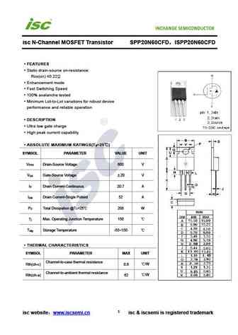
isc N-Channel MOSFET Transistor SPP20N60CFD ISPP20N60CFD FEATURES Static drain-source on-resistance RDS(on) 0.22 Enhancement mode Fast Switching Speed 100% avalanche tested Minimum Lot-to-Lot variations for robust device performance and reliable operation DESCRIPTION Ultra low gate charge High peak current capability ABSOLUTE MAXIMUM RATINGS(T =25 ) a
spw20n60c3.pdf
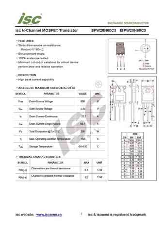
isc N-Channel MOSFET Transistor SPW20N60C3 ISPW20N60C3 FEATURES Static drain-source on-resistance RDS(on) 190m Enhancement mode 100% avalanche tested Minimum Lot-to-Lot variations for robust device performance and reliable operation DESCRITION High peak current capability ABSOLUTE MAXIMUM RATINGS(T =25 ) a SYMBOL PARAMETER VALUE UNIT V Drain-Source Voltage
spw20n60s5.pdf
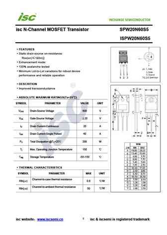
isc N-Channel MOSFET Transistor SPW20N60S5 ISPW20N60S5 FEATURES Static drain-source on-resistance RDS(on) 190m Enhancement mode 100% avalanche tested Minimum Lot-to-Lot variations for robust device performance and reliable operation DESCRITION Improved transconductance ABSOLUTE MAXIMUM RATINGS(T =25 ) a SYMBOL PARAMETER VALUE UNIT V Drain-Source Voltage 60
spb20n60c3.pdf
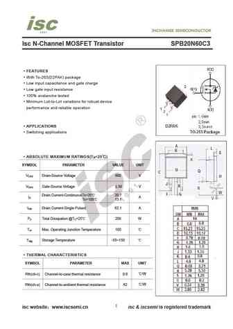
Isc N-Channel MOSFET Transistor SPB20N60C3 FEATURES With To-263(D2PAK) package Low input capacitance and gate charge Low gate input resistance 100% avalanche tested Minimum Lot-to-Lot variations for robust device performance and reliable operation APPLICATIONS Switching applications ABSOLUTE MAXIMUM RATINGS(T =25 ) a SYMBOL PARAMETER VALUE UNIT V Drain-Source Vo
ixkp20n60c5.pdf
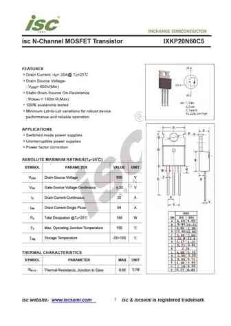
isc N-Channel MOSFET Transistor IXKP20N60C5 FEATURES Drain Current I = 20A@ T =25 D C Drain Source Voltage- V = 600V(Min) DSS Static Drain-Source On-Resistance R = 180m (Max) DS(on) 100% avalanche tested Minimum Lot-to-Lot variations for robust device performance and reliable operation APPLICATIONS Switched mode power supplies Uninterruptible power suppli
spw20n60cfd.pdf
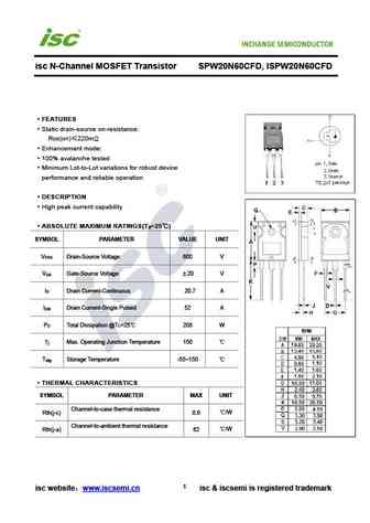
isc N-Channel MOSFET Transistor SPW20N60CFD, ISPW20N60CFD FEATURES Static drain-source on-resistance RDS(on) 220m Enhancement mode 100% avalanche tested Minimum Lot-to-Lot variations for robust device performance and reliable operation DESCRIPTION High peak current capability ABSOLUTE MAXIMUM RATINGS(T =25 ) a SYMBOL PARAMETER VALUE UNIT V Drain-Source Volt
aok20n60l.pdf
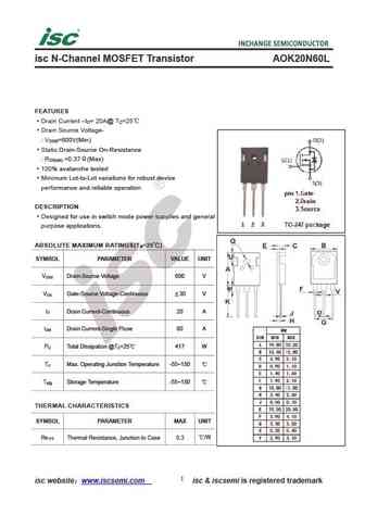
isc N-Channel MOSFET Transistor AOK20N60L FEATURES Drain Current I = 20A@ T =25 D C Drain Source Voltage- V =600V(Min) DSS Static Drain-Source On-Resistance R =0.37 (Max) DS(on) 100% avalanche tested Minimum Lot-to-Lot variations for robust device performance and reliable operation DESCRIPTION Designed for use in switch mode power supplies and general purpo
aot20n60.pdf
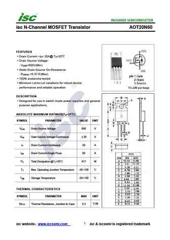
isc N-Channel MOSFET Transistor AOT20N60 FEATURES Drain Current I = 20A@ T =25 D C Drain Source Voltage- V =600V(Min) DSS Static Drain-Source On-Resistance R =0.37 (Max) DS(on) 100% avalanche tested Minimum Lot-to-Lot variations for robust device performance and reliable operation DESCRIPTION Designed for use in switch mode power supplies and general purpos
spi20n60c3.pdf
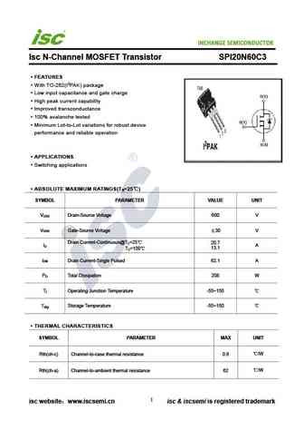
INCHANGE Semiconductor Isc N-Channel MOSFET Transistor SPI20N60C3 FEATURES With TO-262(I2PAK) package Low input capacitance and gate charge High peak current capability Improved transconductance 100% avalanche tested Minimum Lot-to-Lot variations for robust device performance and reliable operation APPLICATIONS Switching applications ABSOLUTE MAXIMUM RATINGS(T =2
fmh20n60s1.pdf
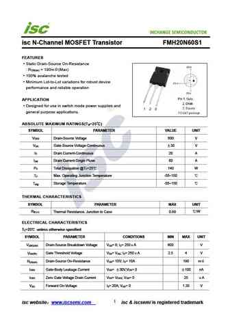
isc N-Channel MOSFET Transistor FMH20N60S1 FEATURES Static Drain-Source On-Resistance R = 190m (Max) DS(on) 100% avalanche tested Minimum Lot-to-Lot variations for robust device performance and reliable operation APPLICATION Designed for use in switch mode power supplies and general purpose applications. ABSOLUTE MAXIMUM RATINGS(T =25 ) a SYMBOL PARAMETER VALUE UNIT V
Otros transistores... 7N60Z, 7N60K, 8N60, 10N60, 10N60K, 12N60, 15N60, 18N60, IRFP064N, 22N60, UF601, UK2996, 1N60A, 1N60, 1N60P, 1N60Z, 2N60L
🌐 : EN ES РУ

Liste
Recientemente añadidas las descripciónes de los transistores:
MOSFET: RM50P30DF | CRTT095N12N | CRSS028N10N | CRST030N10N | CRJQ80N65F | ASDM20N20KQ | ASDM20N100Q | ASDM12N65F | ASDM100R750PKQ | ASDM100R160NKQ | ASDM100R090NP | ASDM100R066NQ | ASDM100R045NQ | ASDM100N34KQ | ASDM100N15KQ | FTF30P35D
Popular searches
2sc2705 | bc239 | 2sc3264 | mp38a | bc546 transistor | bd243 | 2sk170 datasheet | 2n7000 equivalent