9N50 Datasheet. Equivalente. Reemplazo. Hoja de especificaciones. Principales características
Número de Parte: 9N50 📄📄
Tipo de FET: MOSFET
Polaridad de transistor: N
ESPECIFICACIONES MÁXIMAS
Pdⓘ - Máxima disipación de potencia: 44 W
|Vds|ⓘ - Voltaje máximo drenador-fuente: 500 V
|Vgs|ⓘ - Voltaje máximo fuente-puerta: 30 V
|Id|ⓘ - Corriente continua de drenaje: 9 A
Tjⓘ - Temperatura máxima de unión: 150 °C
CARACTERÍSTICAS ELÉCTRICAS
trⓘ - Tiempo de subida: 65 nS
Cossⓘ - Capacitancia de salida: 130 pF
RDSonⓘ - Resistencia estado encendido drenaje a fuente: 0.7 Ohm
Encapsulados: TO-220F
📄📄 Copiar
Búsqueda de reemplazo de 9N50 MOSFET
- Selecciónⓘ de transistores por parámetros
9N50 datasheet
9n50.pdf
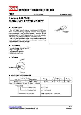
UNISONIC TECHNOLOGIES CO., LTD 9N50 Power MOSFET Preliminary 9 Amps, 500 Volts N-CHANNEL POWER MOSFET DESCRIPTION The UTC 9N50 is an N-channel mode power MOSFET using UTC s advanced technology to provide customers planar stripe and DMOS technology. This technology allows a minimum on-state resistance, superior switching performance. It also can withstand high energy puls
fqp9n50c.pdf
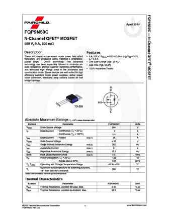
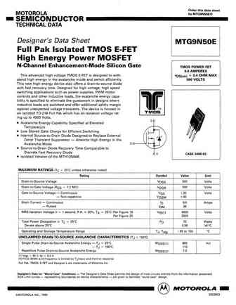
April 2014 FQP9N50C N-Channel QFET MOSFET 500 V, 9 A, 800 m Description Features These N-Channel enhancement mode power field effect 9 A, 500 V, RDS(on) = 800 m (Max.) @ VGS = 10 V, transistors are produced using Fairchild s proprietary, ID = 4.5 A planar stripe, DMOS technology. This advanced Low Gate Charge (Typ. 28 nC) technology has been especially tailored to minim
fqpf9n50ydtu fqpf9n50 fqpf9n50t.pdf

April 2000 TM QFET QFET QFET QFET 500V N-ChanneI MOSFET GeneraI Description Features These N-Channel enhancement mode power field effect 5.3A, 500V, RDS(on) = 0.73 @VGS = 10 V transistors are produced using Fairchild s proprietary, Low gate charge ( typical 28 nC) planar stripe, DMOS technology. Low Crss ( typical 20 pF) This advanced technology has been
fqa9n50.pdf
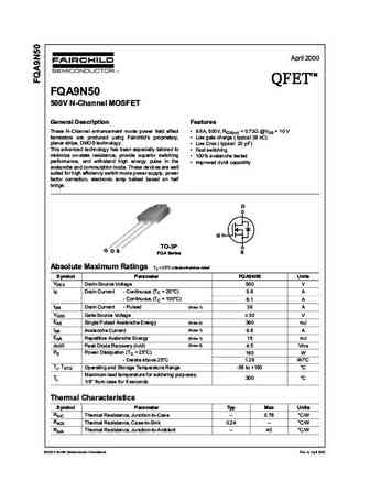
April 2000 TM QFET QFET QFET QFET 500V N-ChanneI MOSFET GeneraI Description Features These N-Channel enhancement mode power field effect 9.6A, 500V, RDS(on) = 0.73 @VGS = 10 V transistors are produced using Fairchild s proprietary, Low gate charge ( typical 28 nC) planar stripe, DMOS technology. Low Crss ( typical 20 pF) This advanced technology has been e
fqb9n50ctm fqb9n50c fqi9n50c fqi9n50ctu.pdf
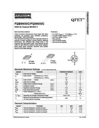
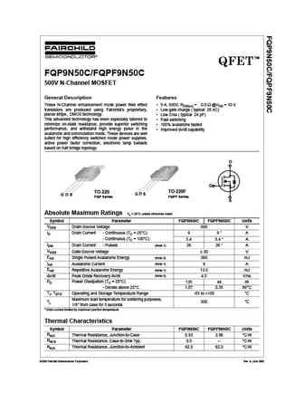
TM QFET FQB9N50C/FQI9N50C 500V N-Channel MOSFET General Description Features These N-Channel enhancement mode power field effect 9 A, 500V, RDS(on) = 0.8 @VGS = 10 V transistors are produced using Fairchild s proprietary, Low gate charge ( typical 28 nC) planar stripe, DMOS technology. Low Crss ( typical 24 pF) This advanced technology has been especially tailored to
fqb9n50cftm.pdf
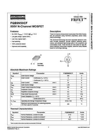
October 2006 TM FRFET FQB9N50CF 500V N-Channel MOSFET Features Description 9A, 500V, RDS(on) = 0.85 @VGS = 10 V These N-Channel enhancement mode power field effect transis- tors are produced using Fairchild s proprietary, planar stripe, Low gate charge ( typical 28nC) DMOS technology. Low Crss ( typical 24pF) This advanced technology has been especially tailored to
fqp9n50.pdf
April 2000 TM QFET QFET QFET QFET 500V N-ChanneI MOSFET GeneraI Description Features These N-Channel enhancement mode power field effect 9.0A, 500V, RDS(on) = 0.73 @VGS = 10 V transistors are produced using Fairchild s proprietary, Low gate charge ( typical 28 nC) planar stripe, DMOS technology. Low Crss ( typical 20 pF) This advanced technology has been e
fqpf9n50ct fqpf9n50cydtu.pdf

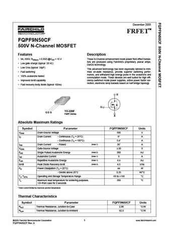
TM QFET FQP9N50C/FQPF9N50C 500V N-Channel MOSFET General Description Features These N-Channel enhancement mode power field effect 9 A, 500V, RDS(on) = 0.8 @VGS = 10 V transistors are produced using Fairchild s proprietary, Low gate charge ( typical 28 nC) planar stripe, DMOS technology. Low Crss ( typical 24 pF) This advanced technology has been especially tailored to
fqpf9n50cf.pdf
December 2005 TM FRFET FQPF9N50CF 500V N-Channel MOSFET Features Description 9A, 500V, RDS(on) = 0.85 @VGS = 10 V These N-Channel enhancement mode power field effect transis- tors are produced using Fairchild s proprietary, planar stripe, Low gate charge (typical 28 nC) DMOS technology. Low Crss (typical 24pF) This advanced technology has been especially tailored to
fqb9n50tm fqi9n50tu.pdf
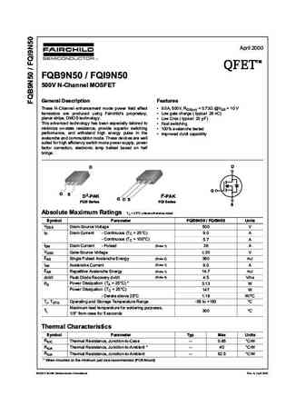
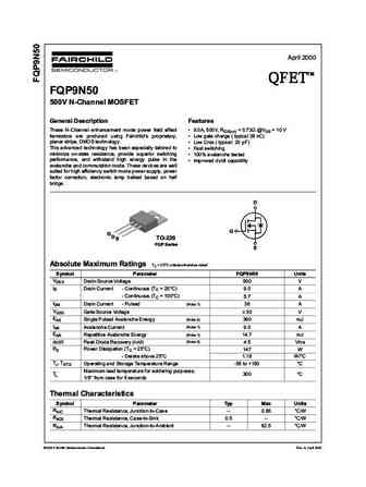
April 2000 TM QFET QFET QFET QFET FQB9N50 / FQI9N50 500V N-ChanneI MOSFET GeneraI Description Features These N-Channel enhancement mode power field effect 9.0A, 500V, RDS(on) = 0.73 @VGS = 10 V transistors are produced using Fairchild s proprietary, Low gate charge ( typical 28 nC) planar stripe, DMOS technology. Low Crss ( typical 20 pF) This advanced technology
fqaf9n50.pdf
April 2000 TM QFET QFET QFET QFET 500V N-ChanneI MOSFET GeneraI Description Features These N-Channel enhancement mode power field effect 7.2A, 500V, RDS(on) = 0.73 @VGS = 10 V transistors are produced using Fairchild s proprietary, Low gate charge ( typical 28 nC) planar stripe, DMOS technology. Low Crss ( typical 20 pF) This advanced technology has been
fqp9n50c fqpf9n50c.pdf
TM QFET FQP9N50C/FQPF9N50C 500V N-Channel MOSFET General Description Features These N-Channel enhancement mode power field effect 9 A, 500V, RDS(on) = 0.8 @VGS = 10 V transistors are produced using Fairchild s proprietary, Low gate charge ( typical 28 nC) planar stripe, DMOS technology. Low Crss ( typical 24 pF) This advanced technology has been especially tailored to
fqpf9n50c.pdf
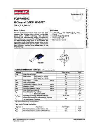
November 2013 FQPF9N50C N-Channel QFET MOSFET 500 V, 9 A, 800 m Description Features These N-Channel enhancement mode power field effect 9 A, 500 V, RDS(on) = 800 m (Max.) @ VGS = 10 V, transistors are produced using Fairchild s proprietary, ID = 4.5 A planar stripe, DMOS technology. This advanced Low Gate Charge (Typ. 28 nC) technology has been especially tailored to m
zxtd09n50de6.pdf
A Product Line of Diodes Incorporated ZXTD09N50DE6 50V DUAL NPN LOW SATURATION SWITCHING TRANSISTOR IN SOT26 Features Mechanical Data BVCEO > 50V Case SOT26 IC = 1A High Continuous Current Case Material Molded Plastic, Green Molding Compound; High Gain UL Flammability Classification Rating 94V-0 RSAT = 160m for Low Equivalent On Resistance
zxtd09n50de6 d619sot23-6.pdf
ZXTD09N50DE6 E6 SuperSOT DUAL 50V NPN SILICON LOW SATURATION SWITCHING TRANSISTOR SUMMARY VCEO=50V; RSAT = 160m ; IC= 1A DESCRIPTION A dual NPN low saturation transistor combination contained in a single 6 lead SOT23 package. Each transistor is the equivalent to the ZUMT619 device. FEATURES SOT23-6 Low Equivalent On Resistance Low Saturation Voltage IC=1A Continuous Col
fqb9n50c.pdf

Is Now Part of To learn more about ON Semiconductor, please visit our website at www.onsemi.com Please note As part of the Fairchild Semiconductor integration, some of the Fairchild orderable part numbers will need to change in order to meet ON Semiconductor s system requirements. Since the ON Semiconductor product management systems do not have the ability to manage part nomenclatur
fqpf9n50cf.pdf

Is Now Part of To learn more about ON Semiconductor, please visit our website at www.onsemi.com Please note As part of the Fairchild Semiconductor integration, some of the Fairchild orderable part numbers will need to change in order to meet ON Semiconductor s system requirements. Since the ON Semiconductor product management systems do not have the ability to manage part nomenclatur
tsm9n50ci tsm9n50cz.pdf
Preliminary TSM9N50 500V N-Channel Power MOSFET TO-220 ITO-220 Pin Definition PRODUCT SUMMARY 1. Gate 2. Drain VDS (V) RDS(on)( ) ID (A) 3. Source 500 0.85 @ VGS =10V 4.8 General Description The TSM9N50 N-Channel enhancement mode Power MOSFET is produced by planar stripe DMOS technology. This advanced technology has been especially tailored to minimize on-state resista
kf9n50p-f.pdf
KF9N50P/F SEMICONDUCTOR N CHANNEL MOS FIELD TECHNICAL DATA EFFECT TRANSISTOR General Description KF9N50P This planar stripe MOSFET has better characteristics, such as fast switching time, low on resistance, low gate charge and excellent DIM avalanche characteristics. It is mainly suitable for electronic ballast and switching mode power supplies. FEATURES VDSS(Min.)= 500V, ID= 9
kq9n50p f.pdf
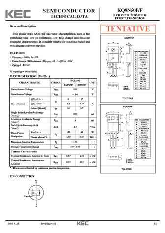
KQ9N50P/F SEMICONDUCTOR N CHANNEL MOS FIELD TECHNICAL DATA EFFECT TRANSISTOR General Description TENTATIVE This planar stripe MOSFET has better characteristics, such as fast switching time, low on resistance, low gate charge and excellent KQ9N50P avalanche characteristics. It is mainly suitable for electronic ballast and A O C switching mode power supplies. F E DIM MILLIMETERS
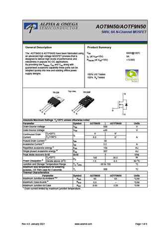
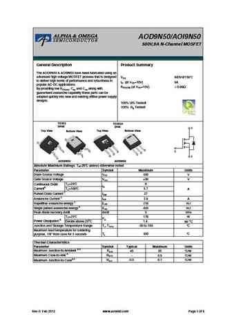
aod9n50 aoi9n50.pdf

AOD9N50/AOI9N50 500V,9A N-Channel MOSFET General Description Product Summary The AOD9N50 & AOI9N50 have been fabricated using an advanced high voltage MOSFET process that is designed VDS 600V@150 to deliver high levels of performance and robustness in ID (at VGS=10V) 9A popular AC-DC applications. RDS(ON) (at VGS=10V)
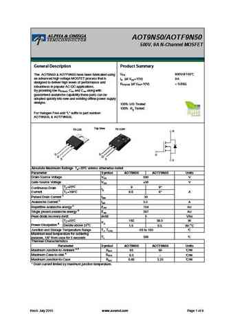
aot9n50 aotf9n50.pdf
AOT9N50/AOTF9N50 500V, 9A N-Channel MOSFET General Description Product Summary VDS 600V@150 The AOT9N50 & AOTF9N50 have been fabricated using an advanced high voltage MOSFET process that is ID (at VGS=10V) 9A designed to deliver high levels of performance and RDS(ON) (at VGS=10V)
aod9n50.pdf
AOD9N50/AOI9N50 500V,9A N-Channel MOSFET General Description Product Summary The AOD9N50 & AOI9N50 have been fabricated using an advanced high voltage MOSFET process that is designed VDS 600V@150 to deliver high levels of performance and robustness in ID (at VGS=10V) 9A popular AC-DC applications. RDS(ON) (at VGS=10V)
aotf9n50.pdf
AOT9N50/AOTF9N50 500V, 9A N-Channel MOSFET General Description Product Summary VDS 600V@150 The AOT9N50 & AOTF9N50 have been fabricated using an advanced high voltage MOSFET process that is ID (at VGS=10V) 9A designed to deliver high levels of performance and RDS(ON) (at VGS=10V)
aoi9n50.pdf

AOD9N50/AOI9N50 500V,9A N-Channel MOSFET General Description Product Summary The AOD9N50 & AOI9N50 have been fabricated using an advanced high voltage MOSFET process that is designed VDS 600V@150 to deliver high levels of performance and robustness in ID (at VGS=10V) 9A popular AC-DC applications. RDS(ON) (at VGS=10V)
aot9n50.pdf

AOT9N50/AOTF9N50 500V, 9A N-Channel MOSFET General Description Product Summary VDS 600V@150 The AOT9N50 & AOTF9N50 have been fabricated using an advanced high voltage MOSFET process that is ID (at VGS=10V) 9A designed to deliver high levels of performance and RDS(ON) (at VGS=10V)
ap09n50i-hf.pdf
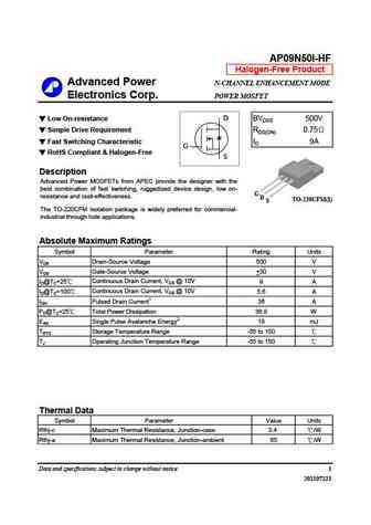
AP09N50I-HF Halogen-Free Product Advanced Power N-CHANNEL ENHANCEMENT MODE Electronics Corp. POWER MOSFET D Low On-resistance BVDSS 500V Simple Drive Requirement RDS(ON) 0.75 Fast Switching Characteristic ID 9A G RoHS Compliant & Halogen-Free S Description Advanced Power MOSFETs from APEC provide the designer with the best combination of fast switching, ruggedized
ap09n50i.pdf
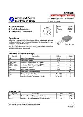
AP09N50I RoHS-compliant Product Advanced Power N-CHANNEL ENHANCEMENT MODE Electronics Corp. POWER MOSFET D Low On-resistance BVDSS 500V Simple Drive Requirement RDS(ON) 0.75 Fast Switching Characteristic ID 9A G S Description Advanced Power MOSFETs from APEC provide the designer with the best combination of fast switching, ruggedized device design, low on- G resistan
ap09n50p-hf.pdf
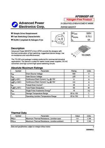
AP09N50P-HF Halogen-Free Product Advanced Power N-CHANNEL ENHANCEMENT MODE Electronics Corp. POWER MOSFET D Simple Drive Requirement BVDSS 500V Fast Switching Characteristic RDS(ON) 0.75 RoHS Compliant & Halogen-Free ID 9A G S Description Advanced Power MOSFETs from APEC provide the designer with the best combination of fast switching, ruggedized device design, low G
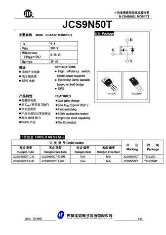
jcs9n50ct jcs9n50ft.pdf
N R N-CHANNEL MOSFET JCS9N50T Package MAIN CHARACTERISTICS ID 9 A VDSS 500 V Rdson-max 0.75 @Vgs=10V Qg-typ 29 nC APPLICATIONS High efficiency switch mode power supplies Electronic lamp ballasts UPS based on half bridge
jcs9n50vc jcs9n50rc jcs9n50cc jcs9n50fc.pdf
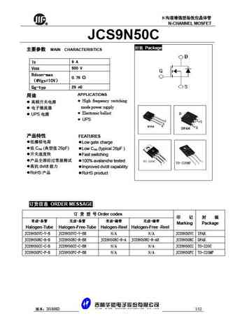
N R N-CHANNEL MOSFET JCS9N50C Package MAIN CHARACTERISTICS ID 9 A VDSS 500 V Rdson-max 0.75 @Vgs=10V Qg-typ 29 nC APPLICATIONS High frequency switching mode power supply Electronic ballast UPS UPS FEATURE
mtn9n50fp.pdf
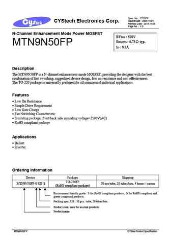
Spec. No. C720FP Issued Date 2009.10.01 CYStech Electronics Corp. Revised Date 2014.11.06 Page No. 1/ 9 N-Channel Enhancement Mode Power MOSFET BVDSS 500V RDS(ON) 0.78 typ. MTN9N50FP ID 8.5A Description The MTN9N50FP is a N-channel enhancement-mode MOSFET, providing the designer with the best combination of fast switching, ruggedized device design, low on
itp09n50a.pdf
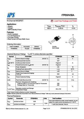
ITP09N50A N-Channel MOSFET Pb Lead Free Package and Finish Applications VDSS RDS(ON) (Typ.) ID Adaptor Charger 500 V 0.55 9.0 A SMPS Standby Power Features RoHS Compliant D Low ON Resistance Low Gate Charge Peak Current vs Pulse Width Curve G G D S Ordering Information PART NUMBER PACKAGE BRAND TO-220 S Not to Scale ITP09N50A TO-220 ITP0
kqb9n50.pdf
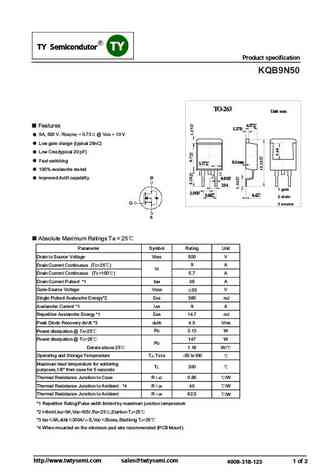
SMD Type IC SMD Type IC SMD Type IC SMD Type IC SMD Type IC SMD Type IC SMD Type IC SMD Type Transistors SMD Type Transistors SMD Type Transistors SMD Type Transistors SMD Type Transistors SMD Type Transistors SMD Type Transistors SMDType SMDType IC Product specification KQB9N50 TO-263 Unit mm 4.57+0.2 Features -0.2 +0.1 1.27-0.1 9A, 500 V. RDS(ON) =0.73 @VGS =10 V Low
mdf9n50bth mdp9n50bth.pdf
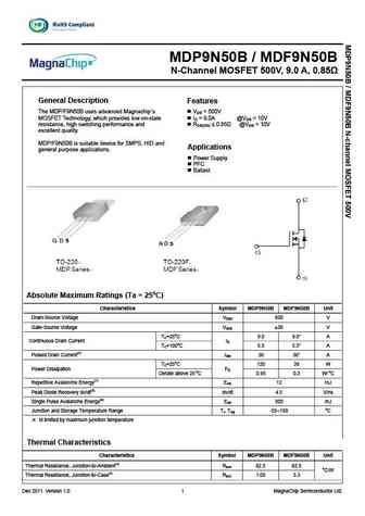
MDP9N50B / MDF9N50B N-Channel MOSFET 500V, 9.0 A, 0.85 General Description Features The MDP/F9N50B uses advanced Magnachip s VDS = 500V MOSFET Technology, which provides low on-state ID = 9.0A @VGS = 10V resistance, high switching performance and RDS(ON) 0.85 @VGS = 10V excellent quality. MDP/F9N50B is suitable device for SMPS, HID and Applications general purpo
mdf9n50fth.pdf
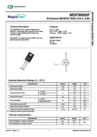
MDF9N50F N-Channel MOSFET 500V, 8.0 A, 0.9 General Description Features The MDF9N50F uses advanced Magnachip s V = 500V DS MOSFET Technology, which provides low on-state I = 8.0A @V = 10V D GS resistance, high switching performance and RDS(ON) 0.9 @VGS = 10V excellent quality. Applications MDF9N50F is suitable device for SMPS, HID and general purp
mdp9n50th.pdf
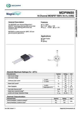
MDP9N50 N-Channel MOSFET 500V, 9.0 A, 0.85 General Description Features The MDP9N50 uses advanced Magnachip s V = 500V DS MOSFET Technology, which provides low on-state ID = 9.0A @VGS = 10V resistance, high switching performance and R
sfp9n50.pdf
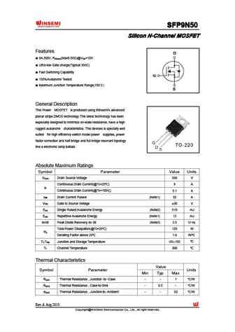
SFP9N50 SFP9N50 SFP9N50 SFP9N50 Silicon N-Channel MOSFET Silicon N-Channel MOSFET Silicon N-Channel MOSFET Silicon N-Channel MOSFET Features 9A,500V, R (Max0.85 )@V =10V DS(on) GS Ultra-low Gate charge(Typical 30nC) Fast Switching Capability 100%Avalanche Tested Maximum Junction Temperature Range(150 ) General Description This Power MOSFET is produced usi
wff9n50.pdf
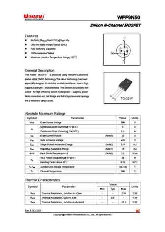
WFF9N50 WFF9N50 WFF9N50 WFF9N50 Silicon N-Channel MOSFET Silicon N-Channel MOSFET Silicon N-Channel MOSFET Silicon N-Channel MOSFET Features 9A,500V, R (Max0.75 )@V =10V DS(on) GS Ultra-low Gate charge(Typical 30nC) Fast Switching Capability 100%Avalanche Tested Maximum Junction Temperature Range(150 ) General Description This Power MOSFET is produced usi
bl9n50-p bl9n50-a bl9n50-u bl9n50-d.pdf
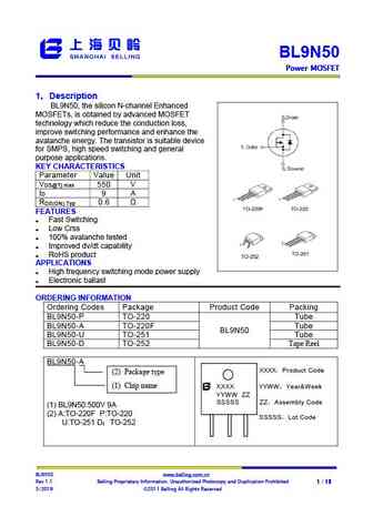
BL9N50 Power MOSFET Power MOSFET Power MOSFET Power MOSFET 1 Description BL9N50, the silicon N-channel Enhanced MOSFETs, is obtained by advanced MOSFET technology which reduce the conduction loss, improve switching performance and enhance the avalanche energy. The transistor is suitable device for SMPS, high speed switching and general purpose applications.
gpt09n50-d-g.pdf
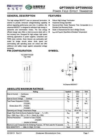
GPT09N50 GPT09N50D POWER FIELD EFFECT TRANSISTOR GENERAL DESCRIPTION FEATURES This high voltage MOSFET uses an advanced termination Robust High Voltage Termination scheme to provide enhanced voltage-blocking capability Avalanche Energy Specified without degrading performance over time. In addition, this Source-to-Drain Diode Recovery Time Comparable to a advanced MOSFET is des
jfpc9n50c jffm9n50c.pdf
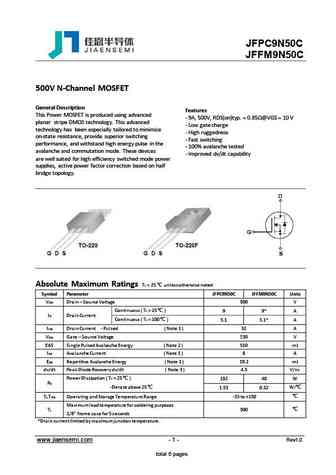
JFPC9N50C JFFM9N50C 500V N-Channel MOSFET General Description Features This Power MOSFET is produced using advanced - 9A, 500V, RDS(on)typ. = 0.85 @VGS = 10 V planar stripe DMOS technology. This advanced - Low gate charge technology has been especially tailored to minimize - High ruggedness on-state resistance, provide superior switching - Fast switching performance,
ptp09n50 pta09n50.pdf
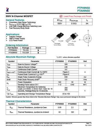
PTP09N50 PTA09N50 500V N-Channel MOSFET General Features BVDSS RDS(ON),typ. ID Proprietary New Planar Technology 500V 0.55 9A RDS(ON),typ.=0.55 @VGS=10V Low Gate Charge Minimize Switching Loss Fast Recovery Body Diode Applications Adaptor Charger SMPS Power Supply LCD Panel Power Ordering Information Part Number Package Brand PTP09N50
swf9n50d swp9n50d swd9n50d.pdf
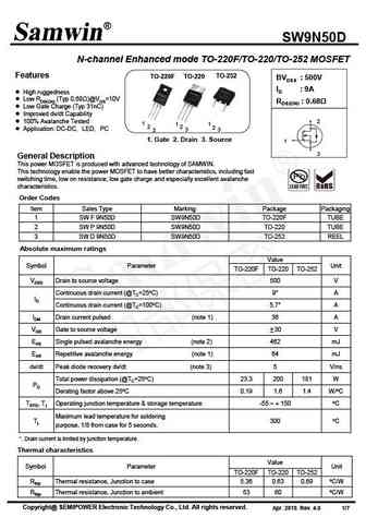
SW9N50D N-channel Enhanced mode TO-220F/TO-220/TO-252 MOSFET Features TO-252 TO-220F TO-220 BVDSS 500V ID 9A High ruggedness Low RDS(ON) (Typ 0.68 )@VGS=10V RDS(ON) 0.68 Low Gate Charge (Typ 31nC) Improved dv/dt Capability 100% Avalanche Tested 2 1 1 1 2 2 2 Application DC-DC LED PC 3 3 3 1. Gate 2. Drain 3. Source
hfp9n50.pdf
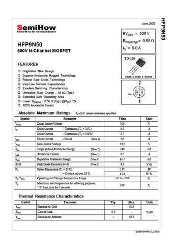
June 2005 BVDSS = 500 V RDS(on) typ HFP9N50 ID = 9.0 A 500V N-Channel MOSFET TO-220 FEATURES Originative New Design 1 2 3 Superior Avalanche Rugged Technology 1.Gate 2. Drain 3. Source Robust Gate Oxide Technology Very Low Intrinsic Capacitances Excellent Switching Characteristics Unrivalled Gate Charge 35 nC (Typ.) Extended Safe Operating Area Lower RDS(O
hfw9n50.pdf
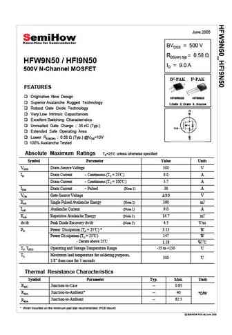
June 2005 BVDSS = 500 V RDS(on) typ HFW9N50 / HFI9N50 ID = 9.0 A 500V N-Channel MOSFET D2-PAK I2-PAK FEATURES Originative New Design HFW9N50 HFI9N50 Superior Avalanche Rugged Technology 1.Gate 2. Drain 3. Source Robust Gate Oxide Technology Very Low Intrinsic Capacitances Excellent Switching Characteristics Unrivalled Gate Charge 35 nC (Typ.) Extended Safe Op
hfs9n50.pdf
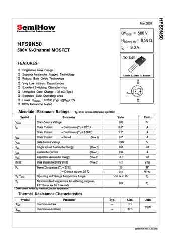
Mar 2008 BVDSS = 500 V RDS(on) typ HFS9N50 ID = 9.0 A 500V N-Channel MOSFET TO-220F FEATURES 1 Originative New Design 2 3 Superior Avalanche Rugged Technology 1.Gate 2. Drain 3. Source Robust Gate Oxide Technology Very Low Intrinsic Capacitances Excellent Switching Characteristics Unrivalled Gate Charge 35 nC (Typ.) Extended Safe Operating Area Lower RDS(
msk9n50f msk9n50t.pdf
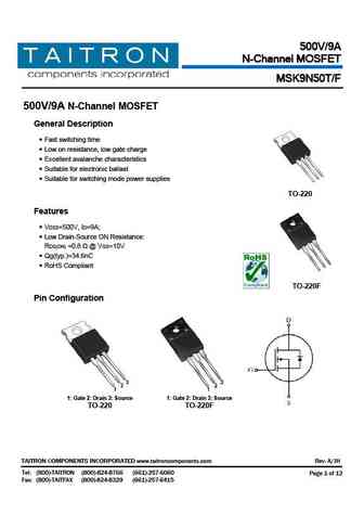
500V/9A N-Channel MOSFET MSK9N50T/F 500V/9A N-Channel MOSFET General Description Fast switching time Low on resistance, low gate charge Excellent avalanche characteristics Suitable for electronic ballast Suitable for switching mode power supplies TO-220 Features VDSS=500V, ID=9A; Low Drain-Source ON Resistance RDS(ON) =0.8 @ VGS=10V
tmp9n50 tmpf9n50.pdf
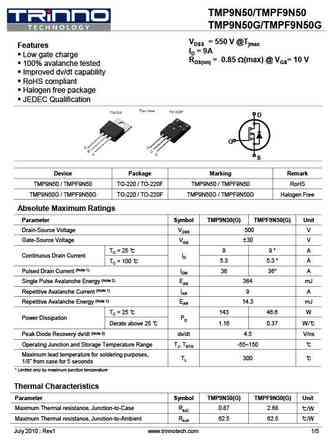
TMP9N50/TMPF9N50 TMP9N50G/TMPF9N50G VDSS = 550 V @Tjmax Features ID = 9A Low gate charge RDS(on) = 0.85 W(max) @ VGS= 10 V 100% avalanche tested Improved dv/dt capability RoHS compliant Halogen free package JEDEC Qualification D G S Device Package Marking Remark TMP9N50 / TMPF9N50 TO-220 / TO-220F TMP9N50 / TMPF9N50 RoHS TMP9N50G / TMPF9N50G TO-220 / T
tmp9n50s tmpf9n50s.pdf
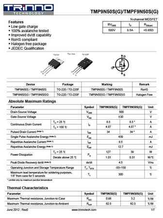
TMP9N50S(G)/TMPF9N50S(G) N-channel MOSFET Features BVDSS ID RDS(on) Low gate charge 500V 8.5A
qm09n50f.pdf
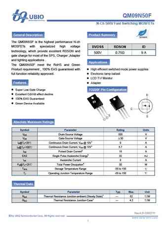
QM09N50F 1 2011-06-15 - 1 - N-Ch 500V Fast Switching MOSFETs General Description Product Summery The QM09N50F is the highest performance N-ch MOSFETs with specialized high voltage BVDSS RDSON ID technology, which provide excellent RDSON and 500V 0.75 9 A gate charge for most of the SPS, Charger ,Adapter and lighting applications . Applications The QM09N50F m
wmk9n50d1b wml9n50d1b wmo9n50d1b.pdf
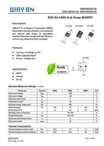
WMK9N50D1B WML9N50D1B WMO9N50D1B 500V 9A 0.68 N-ch Power MOSFET Description TO-252 TO-220 TO-220F WMOSTM D1 is Wayon s 1st generation VDMOS TAB TAB family that is dramatic reduction in on-resistance and ultra-low gate charge for applications requiring high power density and high efficiency. D G And it is very robust and RoHS compliant. S G D S G D S
fir9n50fg.pdf
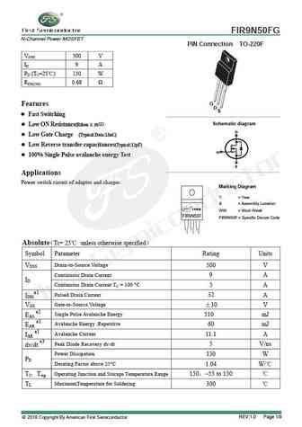
FIR9N50FG N-Channel Power MOSFET PIN Connection TO-220F VDSS 500 V ID 9 A PD (TC=25 ) 130 W RDS(ON) 0.68 G Features D S Fast Switching g Schematic dia ram ) Low ON Resistance(Rdson 0.85 D Low Gate Charge (Typical Data 13nC) Low Reverse transfer capacitances(Typical 12pF) G 100% Single Pulse avalanche energy Test S Applications Power switch circu
spc9n50g.pdf
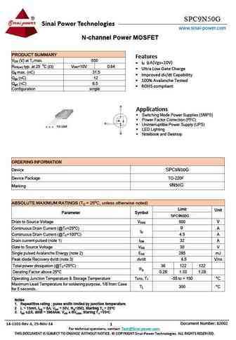
SPC9N50G Sinai Power Technologies www.sinai-power.com N-channel Power MOSFET PRODUCT SUMMARY Features V (V) at T max. 550 DS J A(Vgs=10V) ID 9 o R typ. at 25 C ( ) V =10V 0.64 DS(on) GS Ultra Low Gate Charge Q max. (nC) 31.5 g Improved dv/dt Capability Q (nC) 12 gs 100% Avalanche Tested Q (nC) 6.5 gd ROHS compliant Configuration sing
fxn9n50f.pdf
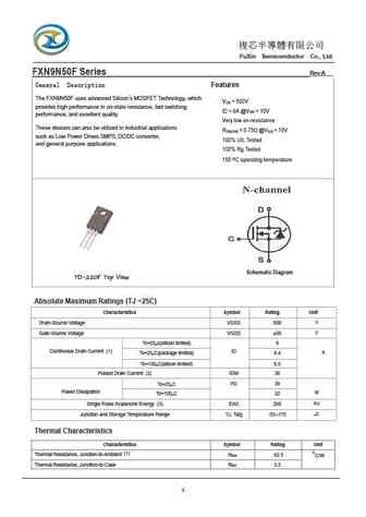
FuXin Semiconductor Co., Ltd. FXN9N50F Series Rev.A General Description Features The FXN9N50F uses advanced Silicon s MOSFET Technology, which V = 500V DS provides high performance in on-state resistance, fast switching ID = 9A @V = 10V GS performance, and excellent quality. Very low on-resistance These devices can also be utilized in industrial appl
mdf9n50bth.pdf
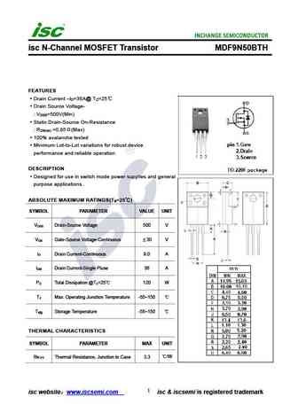
isc N-Channel MOSFET Transistor MDF9N50BTH FEATURES Drain Current I =36A@ T =25 D C Drain Source Voltage- V =500V(Min) DSS Static Drain-Source On-Resistance R =0.85 (Max) DS(on) 100% avalanche tested Minimum Lot-to-Lot variations for robust device performance and reliable operation DESCRIPTION Designed for use in switch mode power supplies and general purpo
aod9n50.pdf
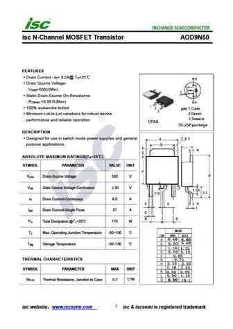
isc N-Channel MOSFET Transistor AOD9N50 FEATURES Drain Current I = 9.0A@ T =25 D C Drain Source Voltage- V =500V(Min) DSS Static Drain-Source On-Resistance R =0.86 (Max) DS(on) 100% avalanche tested Minimum Lot-to-Lot variations for robust device performance and reliable operation DESCRIPTION Designed for use in switch mode power supplies and general purpos
aotf9n50.pdf
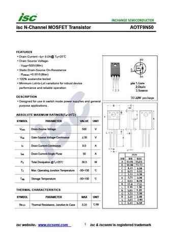
isc N-Channel MOSFET Transistor AOTF9N50 FEATURES Drain Current I = 9.0A@ T =25 D C Drain Source Voltage- V =500V(Min) DSS Static Drain-Source On-Resistance R =0.85 (Max) DS(on) 100% avalanche tested Minimum Lot-to-Lot variations for robust device performance and reliable operation DESCRIPTION Designed for use in switch mode power supplies and general purpo
mdp9n50bth.pdf
isc N-Channel MOSFET Transistor MDP9N50BTH FEATURES Drain Current I = 9A@ T =25 D C Drain Source Voltage V = 500V(Min) DSS Static Drain-Source On-Resistance R = 0.85 (Max) @V = 10V DS(on) GS 100% avalanche tested Minimum Lot-to-Lot variations for robust device performance and reliable operation DESCRIPTION motor drive, DC-DC converter, power switch and solen
aoi9n50.pdf
isc N-Channel MOSFET Transistor AOI9N50 FEATURES Drain Current I = 9.0A@ T =25 D C Drain Source Voltage- V =500V(Min) DSS Static Drain-Source On-Resistance R =0.86 (Max) DS(on) 100% avalanche tested Minimum Lot-to-Lot variations for robust device performance and reliable operation DESCRIPTION Designed for use in switch mode power supplies and general purpos
mdp9n50th.pdf
isc N-Channel MOSFET Transistor MDP9N50TH FEATURES Drain Current I = 9A@ T =25 D C Drain Source Voltage V = 500V(Min) DSS Static Drain-Source On-Resistance R = 0.85 (Max) @V = 10V DS(on) GS 100% avalanche tested Minimum Lot-to-Lot variations for robust device performance and reliable operation DESCRIPTION motor drive, DC-DC converter, power switch and soleno
aot9n50.pdf
isc N-Channel MOSFET Transistor AOT9N50 FEATURES Drain Current I = 9.0A@ T =25 D C Drain Source Voltage- V =500V(Min) DSS Static Drain-Source On-Resistance R =0.85 (Max) DS(on) 100% avalanche tested Minimum Lot-to-Lot variations for robust device performance and reliable operation DESCRIPTION Designed for use in switch mode power supplies and general purpos
apn9n50d.pdf
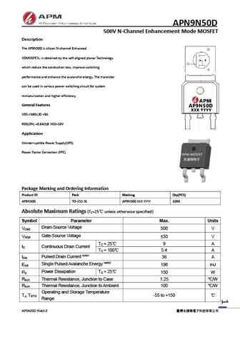
APN9N50D 500V N-Channel Enhancement Mode MOSFET Description The AP9N50D is silicon N-channel Enhanced VDMOSFETs, is obtained by the self-aligned planar Technology which reduce the conduction loss, improve switching performance and enhance the avalanche energy. The transistor can be used in various power switching circuit for system miniaturization and higher efficiency. Gener
Otros transistores... 3N60, 3N60A, 3N60Z, 3N60K, 4N60, 4N60Z, 4N60K, 8N50H, AO3400, 10N50, 11N50, 12N50, 13N50, 14N50, 15N50, 16N50, 18N50
🌐 : EN ES РУ

Liste
Recientemente añadidas las descripciónes de los transistores:
MOSFET: BCD70N07A | BCD90N03 | BCD80N06 | T50N06 | H50N06 | BCD12N65 | BCT12N65 | BCD4N65 | BCT4N65 | BCD7N65 | BCT7N65 | BCT20N65 | ASDM30P100KQ | ASDM30N90Q | ASDM30N75KQ | ASDM30N150Q
Popular searches
2sb560 | tip31c transistor equivalent | 2sc1815 datasheet | mj15015 | 13003 transistor datasheet | 2n3416 | bdx53c | k3563