12N50 Datasheet. Equivalente. Reemplazo. Hoja de especificaciones. Principales características
Número de Parte: 12N50 📄📄
Tipo de FET: MOSFET
Polaridad de transistor: N
ESPECIFICACIONES MÁXIMAS
Pdⓘ - Máxima disipación de potencia: 195 W
|Vds|ⓘ - Voltaje máximo drenador-fuente: 500 V
|Vgs|ⓘ - Voltaje máximo fuente-puerta: 30 V
|Id|ⓘ - Corriente continua de drenaje: 12 A
Tjⓘ - Temperatura máxima de unión: 150 °C
CARACTERÍSTICAS ELÉCTRICAS
trⓘ - Tiempo de subida: 54 nS
Cossⓘ - Capacitancia de salida: 198 pF
RDSonⓘ - Resistencia estado encendido drenaje a fuente: 0.42 Ohm
📄📄 Copiar
Búsqueda de reemplazo de 12N50 MOSFET
- Selecciónⓘ de transistores por parámetros
12N50 datasheet
12n50.pdf
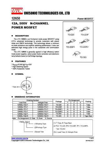
UNISONIC TECHNOLOGIES CO., LTD 12N50 Power MOSFET 12A, 500V N-CHANNEL POWER MOSFET DESCRIPTION The UTC 12N50 is an N-channel mode power MOSFET using UTC s advanced technology to provide customers with planar stripe and DMOS technology. This technology allows a minimum on-state resistance and superior switching performance. It also can withstand high energy pulse in the av
12n50.pdf
isc N-Channel MOSFET Transistor 12N50 FEATURES Drain Current I = 12A@ T =25 D C Drain Source Voltage- V = 500V(Min) DSS Static Drain-Source On-Resistance R = 0.5 (Max) DS(on) Fast Switching Minimum Lot-to-Lot variations for robust device performance and reliable operation APPLICATIONS Switch mode power supply. ABSOLUTE MAXIMUM RATINGS(T =25 ) a SYMBO
hgth12n40c1d hgth12n40e1d hgth12n50c1d hgth12n50e1d.pdf
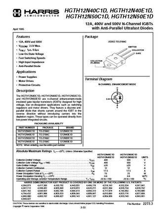
HGTH12N40C1D, HGTH12N40E1D, S E M I C O N D U C T O R HGTH12N50C1D, HGTH12N50E1D 12A, 400V and 500V N-Channel IGBTs with Anti-Parallel Ultrafast Diodes April 1995 Features Package JEDEC TO-218AC 12A, 400V and 500V VCE(ON) 2.5V Max. EMITTER TFALL 1 s, 0.5 s COLLECTOR GATE Low On-State Voltage Fast Switching Speeds COLLECTOR High Input Impedance (FLANG
hgth12n40c1 hgth12n40e1 hgth12n50c1 hgth12n50e1 hgtm12n40c1 hgtm12n40e1 hgtm12n50c1 hgtm12n50e1 hgtp10n40c1 hgtp10n40e1 hgtp10n50c1 hgtp10n50e1.pdf
hgth12n40c1 hgth12n40e1 hgth12n50c1 hgth12n50e1 hgtp10n40c1 hgtp10n40e1 hgtp10n50c1 hgtp10n50e1.pdf
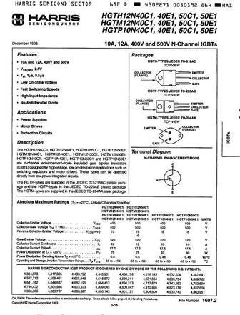
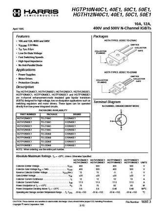
HGTP10N40C1, 40E1, 50C1, 50E1, S E M I C O N D U C T O R HGTH12N40C1, 40E1, 50C1, 50E1 10A, 12A, 400V and 500V N-Channel IGBTs April 1995 Features Packages HGTH-TYPES JEDEC TO-218AC 10A and 12A, 400V and 500V EMITTER VCE(ON) 2.5V Max. COLLECTOR TFI 1 s, 0.5 s GATE COLLECTOR (FLANGE) Low On-State Voltage Fast Switching Speeds High Input Impedance
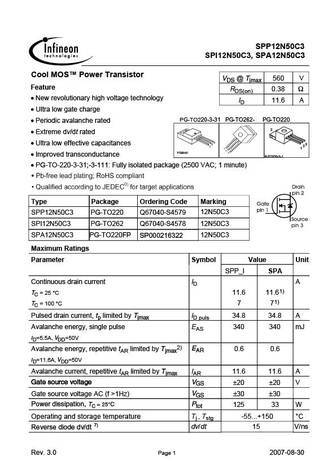
spa12n50c3 spi12n50c3 spp12n50c3.pdf
SPP12N50C3 SPI12N50C3, SPA12N50C3 Cool MOS Power Transistor VDS @ Tjmax 560 V Feature RDS(on) 0.38 New revolutionary high voltage technology ID 11.6 A Ultra low gate charge PG-TO220-3-31 PG-TO262- PG-TO220 Periodic avalanche rated 2 Extreme dv/dt rated 3 Ultra low effective capacitances 2 3 2 1 1 P-TO220-3-31 Improved transconductance P-TO220-3
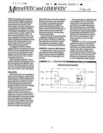
ixth12n45ma ixth12n45mb ixth12n50ma ixth12n50mb ixth15n35ma ixth15n35mb ixth15n40ma ixth15n40mb ixtz42n20mb ixtz67n10ma ixtz67n10mb.pdf
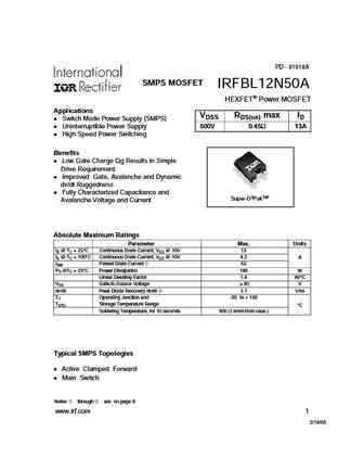
irfbl12n50a.pdf
PD - 91818A SMPS MOSFET IRFBL12N50A HEXFET Power MOSFET Applications VDSS RDS(on) max ID Switch Mode Power Supply (SMPS) Uninterruptible Power Supply 500V 0.45 13A High Speed Power Switching Benefits Low Gate Charge Qg Results in Simple Drive Requirement Improved Gate, Avalanche and Dynamic dv/dt Ruggedness Fully Characterized Capacitance and Super-D2PakTM Avalanche V
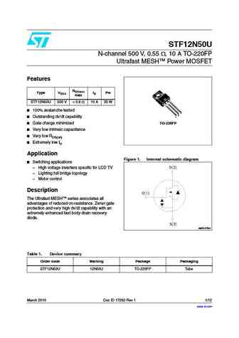
stf12n50u.pdf
STF12N50U N-channel 500 V, 0.55 , 10 A TO-220FP Ultrafast MESH Power MOSFET Features RDS(on) Type VDSS ID Pw max STF12N50U 500 V
stf12n50m2.pdf
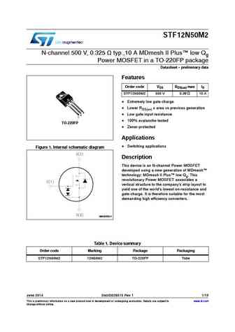
STF12N50M2 N-channel 500 V, 0.325 typ.,10 A MDmesh II Plus low Qg Power MOSFET in a TO-220FP package Datasheet - preliminary data Features Order code VDS RDS(on) max ID STF12N50M2 500 V 0.38 10 A Extremely low gate charge Lower RDS(on) x area vs previous generation 3 2 Low gate input resistance 1 100% avalanche tested TO-220FP Zener-protected Appli
stp12n50m2.pdf
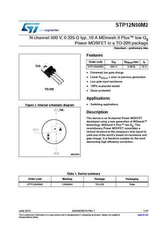
STP12N50M2 N-channel 500 V, 0.325 typ.,10 A MDmesh II Plus low Qg Power MOSFET in a TO-220 package Datasheet - preliminary data Features Order code VDS RDS(on) max ID TAB STP12N50M2 500 V 0.38 10 A Extremely low gate charge Lower RDS(on) x area vs previous generation 3 Low gate input resistance 2 1 100% avalanche tested TO-220 Zener-protected Appl
std12n50m2.pdf
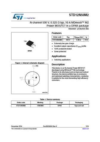
STD12N50M2 N-channel 500 V, 0.325 typ.,10 A MDmesh M2 Power MOSFET in a DPAK package Datasheet - production data Features Order code VDS RDS(on) max ID STD12N50M2 500 V 0.38 10 A TAB Extremely low gate charge 3 Excellent output capacitance (COSS) profile 1 100% avalanche tested DPAK Zener-protected Applications Switching applications Figure 1. Int
fdp12n50nz fdpf12n50nz.pdf
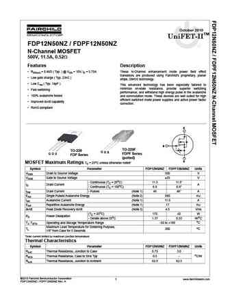
October 2010 UniFET-IITM FDP12N50NZ / FDPF12N50NZ N-Channel MOSFET 500V, 11.5A, 0.52 Features Description RDS(on) = 0.46 ( Typ. ) @ VGS = 10V, ID = 5.75A These N-Channel enhancement mode power field effect transistors are produced using Fairchild s proprietary, planar Low gate charge ( Typ. 23nC ) stripe, DMOS technology. Low Crss ( Typ. 14pF ) This advanced tech
fqb12n50tm am002 fqi12n50tu.pdf
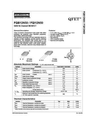
TM QFET FQB12N50 / FQI12N50 500V N-Channel MOSFET General Description Features These N-Channel enhancement mode power field effect 12.1A, 500V, RDS(on) = 0.49 @VGS = 10 V transistors are produced using Fairchild s proprietary, Low gate charge ( typical 39 nC) planar stripe, DMOS technology. Low Crss ( typical 25 pF) This advanced technology has been especially tailored
fdb12n50f.pdf
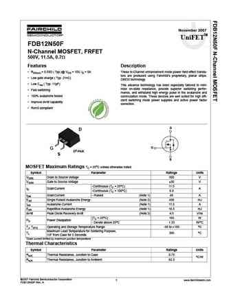
November 2007 UniFETTM FDB12N50F tm N-Channel MOSFET, FRFET 500V, 11.5A, 0.7 Features Description RDS(on) = 0.59 ( Typ.)@ VGS = 10V, ID = 6A These N-Channel enhancement mode power field effect transis- tors are produced using Fairchild s proprietary, planar stripe, Low gate charge ( Typ. 21nC) DMOS technology. Low Crss ( Typ. 11pF) This advance technology has b
fdp12n50 fdpf12n50.pdf
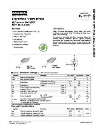
June 2007 UniFETTM FDP12N50 / FDPF12N50 tm N-Channel MOSFET 500V, 11.5A, 0.65 Features Description RDS(on) = 0.55 (Typ.)@ VGS = 10V, ID = 6A These N-Channel enhancement mode power field effect transistors are produced using Fairchild s proprietary, planar Low gate charge ( Typ. 22nC) stripe, DMOS technology. Low Crss ( Typ. 11pF) This advanced technology has be
fdb12n50tm.pdf
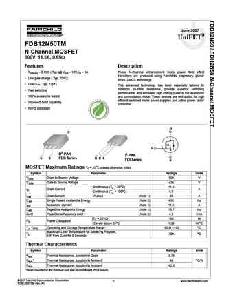
June 2007 UniFETTM FDB12N50TM tm N-Channel MOSFET 500V, 11.5A, 0.65 Features Description RDS(on) = 0.55 ( Typ.)@ VGS = 10V, ID = 6A These N-Channel enhancement mode power field effect transistors are produced using Fairchild s proprietary, planar Low gate charge ( Typ. 22nC) stripe, DMOS technology. Low Crss ( Typ. 12pF) This advanced technology has been especi
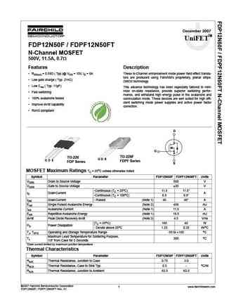
fdp12n50f fdpf12n50ft.pdf
December 2007 UniFETTM FDP12N50F / FDPF12N50FT tm N-Channel MOSFET 500V, 11.5A, 0.7 Features Description RDS(on) = 0.59 ( Typ.)@ VGS = 10V, ID = 6A These N-Channel enhancement mode power field effect transis- tors are produced using Fairchild s proprietary, planar stripe, Low gate charge ( Typ. 21nC) DMOS technology. Low Crss ( Typ. 11pF) This advance technolog
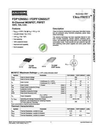
fdp12n50u fdpf12n50ut.pdf
November 2007 Ultra FRFETTM FDP12N50U / FDPF12N50UT tm N-Channel MOSFET, FRFET 500V, 10A, 0.8 Features Description RDS(on) = 0.65 ( Typ.)@ VGS = 10V, ID = 5A These N-Channel enhancement mode power field effect transis- tors are produced using Fairchild s proprietary, planar stripe, Low gate charge ( Typ. 21nC) DMOS technology. Low Crss ( Typ. 11pF) This advance
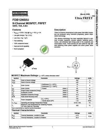
fdb12n50u.pdf
March 2008 TM Ultra FRFET FDB12N50U tm N-Channel MOSFET, FRFET 500V, 10A, 0.8 Features Description RDS(on) = 0.65 ( Typ.)@ VGS = 10V, ID = 5A These N-Channel enhancement mode power field effect transis- tors are produced using Fairchild s proprietary, planar stripe, Low gate charge ( Typ. 21nC) DMOS technology. Low Crss ( Typ. 11pF) This advance technology has
fdpf12n50nzt.pdf
October 2010 UniFET-IITM FDP12N50NZ / FDPF12N50NZ N-Channel MOSFET 500V, 11.5A, 0.52 Features Description RDS(on) = 0.46 ( Typ. ) @ VGS = 10V, ID = 5.75A These N-Channel enhancement mode power field effect transistors are produced using Fairchild s proprietary, planar Low gate charge ( Typ. 23nC ) stripe, DMOS technology. Low Crss ( Typ. 14pF ) This advanced tech
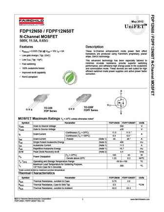
fdp12n50 fdpf12n50t.pdf
May 2012 UniFETTM FDP12N50 / FDPF12N50T tm N-Channel MOSFET 500V, 11.5A, 0.65 Features Description RDS(on) = 0.55 (Typ.)@ VGS = 10V, ID = 6A These N-Channel enhancement mode power field effect transistors are produced using Fairchild s proprietary, planar Low gate charge ( Typ. 22nC) stripe, DMOS technology. Low Crss ( Typ. 11pF) This advanced technology has be
sihb12n50e.pdf
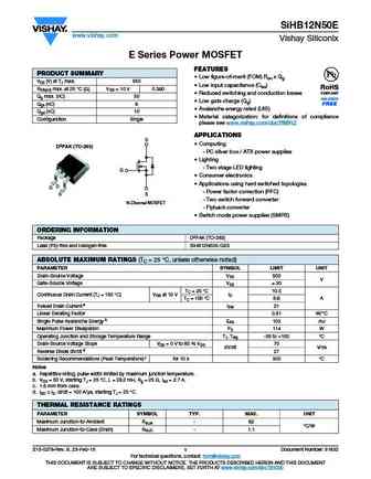
SiHB12N50E www.vishay.com Vishay Siliconix E Series Power MOSFET FEATURES PRODUCT SUMMARY Low figure-of-merit (FOM) Ron x Qg VDS (V) at TJ max. 550 Low input capacitance (Ciss) RDS(on) max. at 25 C ( ) VGS = 10 V 0.380 Reduced switching and conduction losses Qg max. (nC) 50 Low gate charge (Qg) Qgs (nC) 6 Avalanche energy rated (UIS) Qgd (nC) 10 Materi
sihd12n50e.pdf
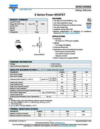
SiHD12N50E www.vishay.com Vishay Siliconix E Series Power MOSFET FEATURES PRODUCT SUMMARY Low figure-of-merit (FOM) Ron x Qg VDS (V) at TJ max. 550 Low input capacitance (Ciss) RDS(on) max. at 25 C ( ) VGS = 10 V 0.380 Reduced switching and conduction losses Qg max. (nC) 50 Low gate charge (Qg) Qgs (nC) 6 Avalanche energy rated (UIS) Qgd (nC) 10 Materi
sihp12n50c sihb12n50c sihf12n50c.pdf
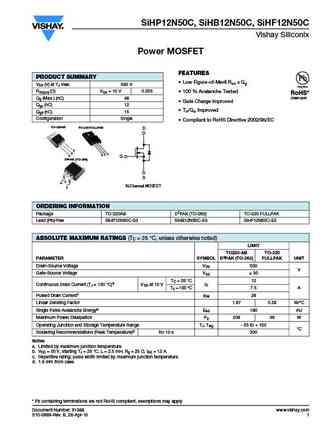
SiHP12N50C, SiHB12N50C, SiHF12N50C Vishay Siliconix Power MOSFET FEATURES PRODUCT SUMMARY Low Figure-of-Merit Ron x Qg VDS (V) at TJ max. 560 V RDS(on) ( )VGS = 10 V 0.555 100 % Avalanche Tested Qg (Max.) (nC) 48 Gate Charge Improved Qgs (nC) 12 Trr/Qrr Improved Qgd (nC) 15 Configuration Single Compliant to RoHS Directive 2002/95/EC TO-220AB TO-220 FULLPAK
sihp12n50e.pdf
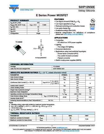
SiHP12N50E www.vishay.com Vishay Siliconix E Series Power MOSFET FEATURES PRODUCT SUMMARY Low figure-of-merit (FOM) Ron x Qg VDS (V) at TJ max. 550 Low input capacitance (Ciss) RDS(on) max. at 25 C ( ) VGS = 10 V 0.380 Reduced switching and conduction losses Qg max. (nC) 50 Low gate charge (Qg) Qgs (nC) 6 Avalanche energy rated (UIS) Qgd (nC) 10 Materi
sihb12n50c sihf12n50c sihp12n50c.pdf
SiHP12N50C, SiHB12N50C, SiHF12N50C Vishay Siliconix Power MOSFET FEATURES PRODUCT SUMMARY Low Figure-of-Merit Ron x Qg VDS (V) at TJ max. 560 V RDS(on) ( )VGS = 10 V 0.555 100 % Avalanche Tested Qg (Max.) (nC) 48 Gate Charge Improved Qgs (nC) 12 Trr/Qrr Improved Qgd (nC) 15 Configuration Single Compliant to RoHS Directive 2002/95/EC TO-220AB TO-220 FULLPAK
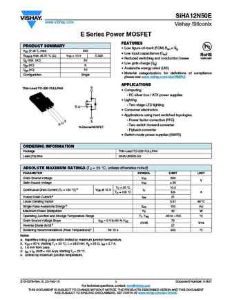
siha12n50e.pdf
SiHA12N50E www.vishay.com Vishay Siliconix E Series Power MOSFET FEATURES PRODUCT SUMMARY Low figure-of-merit (FOM) Ron x Qg VDS (V) at TJ max. 550 Low input capacitance (Ciss) RDS(on) max. at 25 C ( ) VGS = 10 V 0.380 Reduced switching and conduction losses Qg max. (nC) 50 Low gate charge (Qg) Qgs (nC) 6 Avalanche energy rated (UIS) Qgd (nC) 10 Materi
zxt12n50dx.pdf
ZXT12N50DX SuperSOT4 DUAL 50V NPN SILICON LOW SATURATION SWITCHING TRANSISTOR SUMMARY VCEO=50V; RSAT = 45m ; IC= 3A DESCRIPTION This new 4th generation ultra low saturation transistor utilises the Zetex matrix structure combined with advanced assembly techniques to give extremely low on state losses. This makes it ideal for high efficiency, low voltage switching applications. MSOP8
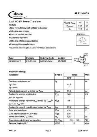
spb12n50c3.pdf
SPB12N50C3 Cool MOS Power Transistor VDS @ Tjmax 560 V Feature RDS(on) 0.38 New revolutionary high voltage technology ID 11.6 A Ultra low gate charge PG-TO263 Periodic avalanche rated Extreme dv/dt rated Ultra low effective capacitances Improved transconductance - Type Package Ordering Code Marking 12N50C3 SPB12N50C3 PG-TO263 Q67040-S4641 Maximum
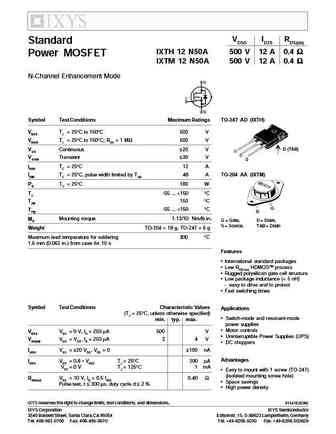
ixth12n50a ixtm12n50a.pdf
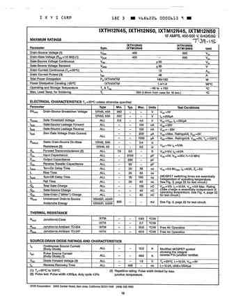
VDSS ID25 RDS(on) Standard IXTH 12 N50A 500 V 12 A 0.4 Power MOSFET IXTM 12 N50A 500 V 12 A 0.4 N-Channel Enhancement Mode Symbol Test Conditions Maximum Ratings TO-247 AD (IXTH) VDSS TJ = 25 C to 150 C 500 V VDGR TJ = 25 C to 150 C; RGS = 1 M 500 V D (TAB) VGS Continuous 20 V VGSM Transient 30 V ID25 TC = 25 C12 A IDM TC
ixti12n50p.pdf
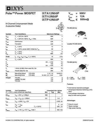
VDSS = 500V PolarTM Power MOSFET IXTA12N50P ID25 = 12A IXTI12N50P RDS(on) 500m IXTP12N50P N-Channel Enhancement Mode Avalanche Rated TO-263 (IXTA) Symbol Test Conditions Maximum Ratings G VDSS TJ = 25 C to 150 C 500 V S (TAB) VDGR TJ = 25 C to 150 C, RGS = 1M 500 V VGSS Continuous 30 V VGSM Transient 40 V Leaded TO-263 (IXTI) ID25
fdpf12n50ft.pdf
Is Now Part of To learn more about ON Semiconductor, please visit our website at www.onsemi.com Please note As part of the Fairchild Semiconductor integration, some of the Fairchild orderable part numbers will need to change in order to meet ON Semiconductor s system requirements. Since the ON Semiconductor product management systems do not have the ability to manage part nomenclatur
fdb12n50f.pdf
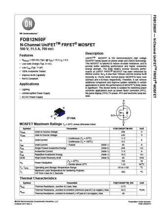
FDB12N50F N-Channel UniFETTM FRFET MOSFET 500 V, 11.5 A, 700 m Description Features UniFETTM MOSFET is ON Semiconductor s high voltage RDS(on) = 590 m (Typ.) @ VGS = 10 V, ID = 6 A MOSFET family based on planar stripe and DMOS technology. This MOSFET is tailored to reduce on-state resistance, and to Low Gate Charge (Typ. 21 nC) provide better switching performa
fdpf12n50ut.pdf
Is Now Part of To learn more about ON Semiconductor, please visit our website at www.onsemi.com Please note As part of the Fairchild Semiconductor integration, some of the Fairchild orderable part numbers will need to change in order to meet ON Semiconductor s system requirements. Since the ON Semiconductor product management systems do not have the ability to manage part nomenclatur
fdb12n50tm.pdf
Is Now Part of To learn more about ON Semiconductor, please visit our website at www.onsemi.com Please note As part of the Fairchild Semiconductor integration, some of the Fairchild orderable part numbers will need to change in order to meet ON Semiconductor s system requirements. Since the ON Semiconductor product management systems do not have the ability to manage part nomenclatur
fdp12n50 fdpf12n50t.pdf
Is Now Part of To learn more about ON Semiconductor, please visit our website at www.onsemi.com Please note As part of the Fairchild Semiconductor integration, some of the Fairchild orderable part numbers will need to change in order to meet ON Semiconductor s system requirements. Since the ON Semiconductor product management systems do not have the ability to manage part nomenclatur
fmc12n50es.pdf
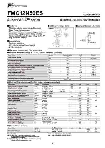
FMC12N50ES FUJI POWER MOSFET Super FAP-E3S series N-CHANNEL SILICON POWER MOSFET Features Outline Drawings [mm] Equivalent circuit schematic Maintains both low power loss and low noise T-Pack (S) Lower R (on) characteristic DS More controllable switching dv/dt by gate resistance Drain(D) Smaller V ringing waveform during switching GS Narrow band of the gate threshold voltage (3.7 0.
fmc12n50e.pdf
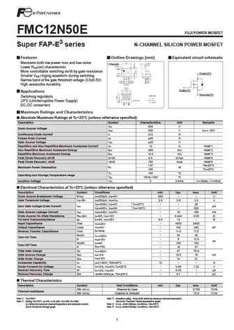
FMC12N50E FUJI POWER MOSFET Super FAP-E3 series N-CHANNEL SILICON POWER MOSFET Features Outline Drawings [mm] Equivalent circuit schematic Maintains both low power loss and low noise T-Pack(S) Lower R (on) characteristic DS More controllable switching dv/dt by gate resistance Drain(D) Smaller V ringing waveform during switching GS Narrow band of the gate threshold voltage (3.0 0.5V)
fmi12n50es.pdf
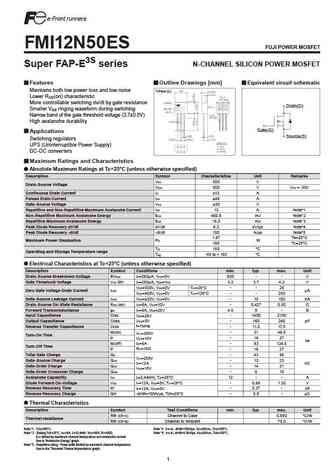
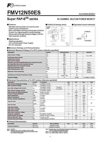
FMI12N50ES FUJI POWER MOSFET Super FAP-E3S series N-CHANNEL SILICON POWER MOSFET Features Outline Drawings [mm] Equivalent circuit schematic Maintains both low power loss and low noise T-Pack (L) Lower R (on) characteristic DS More controllable switching dv/dt by gate resistance Drain(D) Smaller V ringing waveform during switching GS Narrow band of the gate threshold voltage (3.7 0.
fmi12n50e.pdf
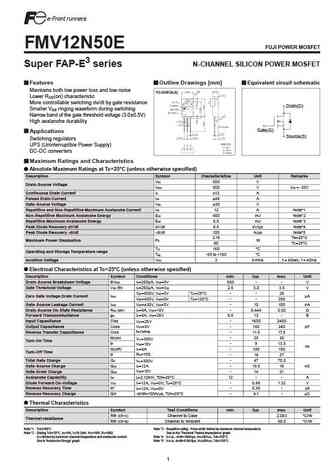
FMI12N50E FUJI POWER MOSFET Super FAP-E3 series N-CHANNEL SILICON POWER MOSFET Features Outline Drawings [mm] Equivalent circuit schematic Maintains both low power loss and low noise T-Pack(L) Lower R (on) characteristic DS More controllable switching dv/dt by gate resistance Drain(D) Smaller V ringing waveform during switching GS Narrow band of the gate threshold voltage (3.0 0.5V)
fmp12n50es.pdf
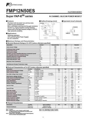
FMP12N50ES FUJI POWER MOSFET Super FAP-E3S series N-CHANNEL SILICON POWER MOSFET Features Outline Drawings [mm] Equivalent circuit schematic Maintains both low power loss and low noise TO-220AB Lower R (on) characteristic DS More controllable switching dv/dt by gate resistance Drain(D) Smaller V ringing waveform during switching GS Narrow band of the gate threshold voltage (3.7 0.5V
fml12n50es.pdf
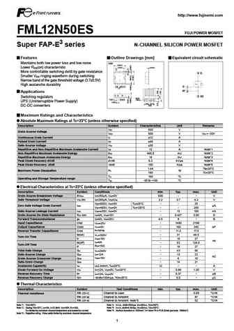
http //www.fujisemi.com FML12N50ES FUJI POWER MOSFET Super FAP-E3 series N-CHANNEL SILICON POWER MOSFET Features Outline Drawings [mm] Equivalent circuit schematic Maintains both low power loss and low noise TFP 9.0 0.2 7.0 0.2 0.4 0.1 Lower R (on) characteristic DS 4 More controllable switching dv/dt by gate resistance 4 D Smaller V ringing waveform during switching GS Narrow
fmv12n50es.pdf
FMV12N50ES FUJI POWER MOSFET Super FAP-E3S series N-CHANNEL SILICON POWER MOSFET Features Outline Drawings [mm] Equivalent circuit schematic Maintains both low power loss and low noise TO-220F (SLS) Lower R (on) characteristic DS More controllable switching dv/dt by gate resistance Drain(D) Smaller V ringing waveform during switching GS Narrow band of the gate threshold voltage (3.
fmp12n50e.pdf
FMP12N50E FUJI POWER MOSFET Super FAP-E3 series N-CHANNEL SILICON POWER MOSFET Features Outline Drawings [mm] Equivalent circuit schematic Maintains both low power loss and low noise TO-220AB Lower R (on) characteristic DS More controllable switching dv/dt by gate resistance Drain(D) Smaller V ringing waveform during switching GS Narrow band of the gate threshold voltage (3.0 0.5V)
fmv12n50e.pdf
FMV12N50E FUJI POWER MOSFET Super FAP-E3 series N-CHANNEL SILICON POWER MOSFET Features Outline Drawings [mm] Equivalent circuit schematic Maintains both low power loss and low noise TO-220F(SLS) Lower R (on) characteristic DS More controllable switching dv/dt by gate resistance Drain(D) Smaller V ringing waveform during switching GS Narrow band of the gate threshold voltage (3.0 0.
msaer12n50a msafr12n50a.pdf
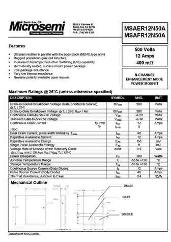
2830 S. Fairview St. Santa Ana, CA 92704 PH (714) 979-8220 MSAER12N50A FAX (714) 966-5256 MSAFR12N50A Features 500 Volts Ultrafast rectifier in parallel with the body diode (MSAE type only) 12 Amps Rugged polysilicon gate cell structure Increased Unclamped Inductive Switching (UIS) capability 400 m Hermetically sealed, surface mount power package Low p
12n50a.pdf
2830 S. Fairview St. Santa Ana, CA 92704 PH (714) 979-8220 MSAER12N50A FAX (714) 966-5256 MSAFR12N50A Features 500 Volts Ultrafast rectifier in parallel with the body diode (MSAE type only) 12 Amps Rugged polysilicon gate cell structure Increased Unclamped Inductive Switching (UIS) capability 400 m Hermetically sealed, surface mount power package Low p
aob12n50l.pdf
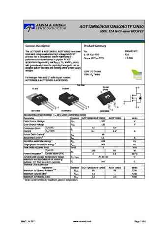
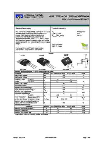
AOT12N50/AOB12N50/AOTF12N50 500V, 12A N-Channel MOSFET General Description Product Summary VDS 600V@150 The AOT12N50 & AOB12N50 & AOTF12N50 have been fabricated using an advanced high voltage MOSFET ID (at VGS=10V) 12A process that is designed to deliver high levels of RDS(ON) (at VGS=10V)
aotf12n50.pdf
AOT12N50/AOB12N50/AOTF12N50 500V, 12A N-Channel MOSFET General Description Product Summary VDS 600V@150 The AOT12N50 & AOB12N50 & AOTF12N50 have been fabricated using an advanced high voltage MOSFET ID (at VGS=10V) 12A process that is designed to deliver high levels of RDS(ON) (at VGS=10V)
aow12n50.pdf
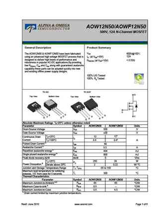
AOW12N50/AOWF12N50 500V, 12A N-Channel MOSFET General Description Product Summary VDS The AOW12N50 & AOWF12N50 have been fabricated 600V@150 12A using an advanced high voltage MOSFET process that is ID (at VGS=10V) designed to deliver high levels of performance and
aowf12n50.pdf
AOW12N50/AOWF12N50 500V, 12A N-Channel MOSFET General Description Product Summary VDS The AOW12N50 & AOWF12N50 have been fabricated 600V@150 12A using an advanced high voltage MOSFET process that is ID (at VGS=10V) designed to deliver high levels of performance and
aot12n50.pdf
AOT12N50/AOB12N50/AOTF12N50 500V, 12A N-Channel MOSFET General Description Product Summary VDS 600V@150 The AOT12N50 & AOB12N50 & AOTF12N50 have been fabricated using an advanced high voltage MOSFET ID (at VGS=10V) 12A process that is designed to deliver high levels of RDS(ON) (at VGS=10V)
aot12n50 aob12n50 aotf12n50.pdf
AOT12N50/AOB12N50/AOTF12N50 500V, 12A N-Channel MOSFET General Description Product Summary VDS 600V@150 The AOT12N50 & AOB12N50 & AOTF12N50 have been fabricated using an advanced high voltage MOSFET ID (at VGS=10V) 12A process that is designed to deliver high levels of RDS(ON) (at VGS=10V)
aow12n50 aowf12n50.pdf
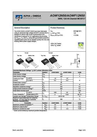
AOW12N50/AOWF12N50 500V, 12A N-Channel MOSFET General Description Product Summary VDS 600V@150 The AOW12N50 & AOWF12N50 have been fabricated using an advanced high voltage MOSFET process that is ID (at VGS=10V) 12A designed to deliver high levels of performance and RDS(ON) (at VGS=10V)
aob12n50.pdf
AOT12N50/AOB12N50/AOTF12N50 500V, 12A N-Channel MOSFET General Description Product Summary VDS 600V@150 The AOT12N50 & AOB12N50 & AOTF12N50 have been fabricated using an advanced high voltage MOSFET ID (at VGS=10V) 12A process that is designed to deliver high levels of RDS(ON) (at VGS=10V)
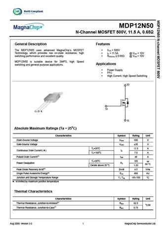
mdp12n50th.pdf
MDP12N50 N-Channel MOSFET 500V, 11.5 A, 0.65 General Description Features The MDP12N50 uses advanced MagnaChip s MOSFET V = 500V DS Technology, which provides low on-state resistance, high I = 11.5A @ V = 10V D GS switching performance and excellent quality. R 0.65 @ V = 10V DS(ON) GS MDP12N50 is suitable device for SMPS, high Speed Applications switching and ge
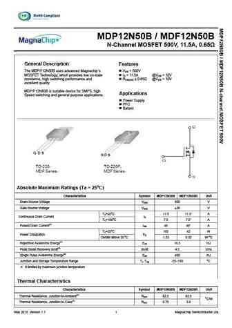
mdf12n50bth mdp12n50bth.pdf
MDP12N50B / MDF12N50B N-Channel MOSFET 500V, 11.5A, 0.65 General Description Features The MDP/F12N50B uses advanced Magnachip s VDS = 500V MOSFET Technology, which provides low on-state ID = 11.5A @VGS = 10V resistance, high switching performance and RDS(ON) 0.65 @VGS = 10V excellent quality. MDP/F12N50B is suitable device for SMPS, high Applications Speed switc
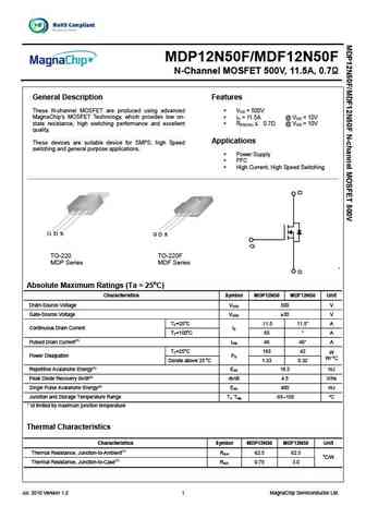
mdf12n50fth mdp12n50fth.pdf
MDP12N50F/MDF12N50F N-Channel MOSFET 500V, 11.5A, 0.7 General Description Features These N-channel MOSFET are produced using advanced V = 500V DS MagnaChip s MOSFET Technology, which provides low on- I = 11.5A @ V = 10V D GS state resistance, high switching performance and excellent R 0.7 @ V = 10V DS(ON) GS quality. Applications These devices are suitable devic
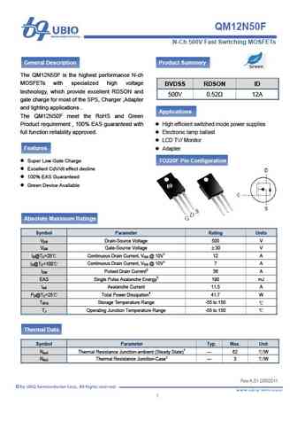
qm12n50f.pdf
QM12N50F 1 2011-07-01 - 1 - N-Ch 500V Fast Switching MOSFETs General Description Product Summery The QM12N50F is the highest performance N-ch MOSFETs with specialized high voltage BVDSS RDSON ID technology, which provide excellent RDSON and 500V 0.52 12A gate charge for most of the SPS, Charger ,Adapter and lighting applications . Applications The QM12N50F m
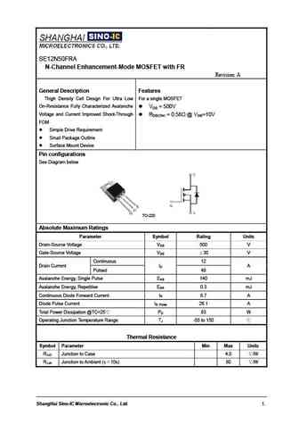
se12n50fra.pdf
SE12N50FRA N-Channel Enhancement-Mode MOSFET with FR Revision A General Description Features Thigh Density Cell Design For Ultra Low For a single MOSFET On-Resistance Fully Characterized Avalanche VDS = 500V Voltage and Current Improved Shoot-Through RDS(ON) = 0.58 @ VGS=10V FOM Simple Drive Requirement Small Package Outline Surface Mount Device
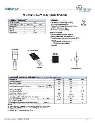
fdb12n50f.pdf
FDB12N50F www.VBsemi.tw Power MOSFET N-Channel 650V (D-S) FEATURES PRODUCT SUMMARY VDS (V) at TJ max. 670 Low figure-of-merit (FOM) Ron x Qg Low input capacitance (Ciss) RDS(on) max. at 25 C ( ) VGS = 10 V 0.67 Reduced switching and conduction losses Qg max. (nC) 41 Ultra low gate charge (Qg) Qgs (nC) 5 Avalanche energy rated (UIS) Qgd (nC) 22 Configurati
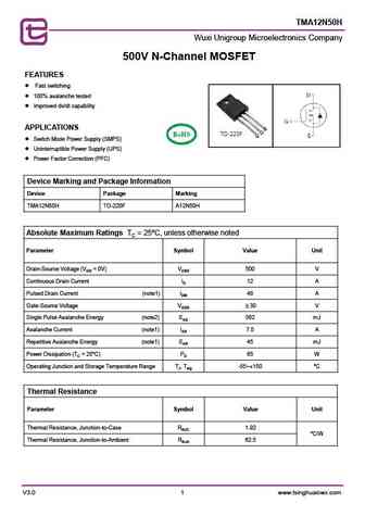
tma12n50h.pdf
TMA12N50H Wuxi Unigroup Microelectronics Company 500V N-Channel MOSFET FEATURES Fast switching 100% avalanche tested Improved dv/dt capability APPLICATIONS Switch Mode Power Supply (SMPS) Uninterruptible Power Supply (UPS) Power Factor Correction (PFC) Device Marking and Package Information Device Package Marking TMA12N50H TO-220F A12N50H Abs
mdp12n50bth.pdf
isc N-Channel MOSFET Transistor MDP12N50BTH FEATURES Drain Current I = 11.5A@ T =25 D C Drain Source Voltage V = 500V(Min) DSS Static Drain-Source On-Resistance R = 0.65 (Max) @V = 10V DS(on) GS 100% avalanche tested Minimum Lot-to-Lot variations for robust device performance and reliable operation DESCRIPTION motor drive, DC-DC converter, power switch and s
aotf12n50.pdf
isc N-Channel MOSFET Transistor AOTF12N50 FEATURES Drain Current I =12A@ T =25 D C Drain Source Voltage- V =500V(Min) DSS Static Drain-Source On-Resistance R = 0.52 (Max) DS(on) 100% avalanche tested Minimum Lot-to-Lot variations for robust device performance and reliable operation DESCRIPTION Designed for use in switch mode power supplies and general purpo
aow12n50.pdf
isc N-Channel MOSFET Transistor AOW12N50 FEATURES Drain Current I =12A@ T =25 D C Drain Source Voltage- V =500V(Min) DSS Static Drain-Source On-Resistance R = 0.52 (Max) DS(on) 100% avalanche tested Minimum Lot-to-Lot variations for robust device performance and reliable operation DESCRIPTION Designed for use in switch mode power supplies and general purpos
mdp12n50th.pdf
isc N-Channel MOSFET Transistor MDP12N50TH FEATURES Drain Current I = 11.5A@ T =25 D C Drain Source Voltage V = 500V(Min) DSS Static Drain-Source On-Resistance R = 0.65 (Max) @V = 10V DS(on) GS 100% avalanche tested Minimum Lot-to-Lot variations for robust device performance and reliable operation DESCRIPTION motor drive, DC-DC converter, power switch and so
aot12n50.pdf
isc N-Channel MOSFET Transistor AOT12N50 FEATURES Drain Current I =12A@ T =25 D C Drain Source Voltage- V =500V(Min) DSS Static Drain-Source On-Resistance R = 0.52 (Max) DS(on) 100% avalanche tested Minimum Lot-to-Lot variations for robust device performance and reliable operation DESCRIPTION Designed for use in switch mode power supplies and general purpos
fmv12n50e.pdf
INCHANGE Semiconductor isc N-Channel MOSFET Transistor FMV12N50E FEATURES With TO-220F packaging High speed switching Very high commutation ruggedness Easy to use 100% avalanche tested Minimum Lot-to-Lot variations for robust device performance and reliable operationz APPLICATIONS Switching applications DC-DC converters Uninterruptible power supply ABSOLUTE
sihd12n50e.pdf
Isc N-Channel MOSFET Transistor SiHD12N50E FEATURES With To-252(DPAK) package Low input capacitance and gate charge Low gate input resistance 100% avalanche tested Minimum Lot-to-Lot variations for robust device performance and reliable operation APPLICATIONS Switching applications ABSOLUTE MAXIMUM RATINGS(T =25 ) a SYMBOL PARAMETER VALUE UNIT V Drain-Source Vol
fdpf12n50nz.pdf
Isc N-Channel MOSFET Transistor FDPF12N50NZ FEATURES With TO-220F package Low input capacitance and gate charge Reduced switching and conduction losses 100% avalanche tested Minimum Lot-to-Lot variations for robust device performance and reliable operation APPLICATIONS Switching applications ABSOLUTE MAXIMUM RATINGS(T =25 ) a SYMBOL PARAMETER VALUE UNIT V Drain-
spp12n50c3.pdf
isc N-Channel MOSFET Transistor SPP12N50C3 ISPP12N50C3 FEATURES Static drain-source on-resistance RDS(on) 0.38 Enhancement mode Fast Switching Speed 100% avalanche tested Minimum Lot-to-Lot variations for robust device performance and reliable operation DESCRITION New revolutionary high voltage technology Ultra low effective capacitance ABSOLUTE MAXIMUM
fdp12n50nz.pdf
Isc N-Channel MOSFET Transistor FDP12N50NZ FEATURES With TO-220F package Low input capacitance and gate charge Reduced switching and conduction losses 100% avalanche tested Minimum Lot-to-Lot variations for robust device performance and reliable operation APPLICATIONS Switching applications ABSOLUTE MAXIMUM RATINGS(T =25 ) a SYMBOL PARAMETER VALUE UNIT V Drain-S
aob12n50.pdf
isc N-Channel MOSFET Transistor AOB12N50 FEATURES Drain Current I =12A@ T =25 D C Drain Source Voltage- V =500V(Min) DSS Static Drain-Source On-Resistance R = 0.52 (Max) DS(on) 100% avalanche tested Minimum Lot-to-Lot variations for robust device performance and reliable operation DESCRIPTION Designed for use in switch mode power supplies and general purpos
spw12n50c3.pdf
isc N-Channel MOSFET Transistor SPW12N50C3 ISPW12N50C3 FEATURES Static drain-source on-resistance RDS(on) 380m Enhancement mode 100% avalanche tested Minimum Lot-to-Lot variations for robust device performance and reliable operation DESCRITION Improved Transconductance ABSOLUTE MAXIMUM RATINGS(T =25 ) a SYMBOL PARAMETER VALUE UNIT V Drain-Source Voltage 50
Otros transistores... 3N60K, 4N60, 4N60Z, 4N60K, 8N50H, 9N50, 10N50, 11N50, IRF3710, 13N50, 14N50, 15N50, 16N50, 18N50, 24N50, 26N50, UF830
Parámetros del MOSFET. Cómo se afectan entre sí.
🌐 : EN ES РУ
Liste
Recientemente añadidas las descripciónes de los transistores:
MOSFET: CEZC2P07 | CEZ2R05 | CEU3133 | CES2361 | CES2312A | CEP100N10L | CEM3425 | CEM3139 | CEM3133 | CEM3115 | CED3133 | CEC3257 | CEC2533 | CEB100N10L | BC3134KT | BC3134K
Popular searches
mj15015 | 13003 transistor datasheet | 2n3416 | bdx53c | k3563 | d882p | 2sb1560 | 2n1304
