14N50 Datasheet. Equivalente. Reemplazo. Hoja de especificaciones. Principales características
Número de Parte: 14N50 📄📄
Tipo de FET: MOSFET
Polaridad de transistor: N
ESPECIFICACIONES MÁXIMAS
Pdⓘ - Máxima disipación de potencia: 150 W
|Vds|ⓘ - Voltaje máximo drenador-fuente: 500 V
|Vgs|ⓘ - Voltaje máximo fuente-puerta: 30 V
|Id|ⓘ - Corriente continua de drenaje: 14 A
Tjⓘ - Temperatura máxima de unión: 150 °C
CARACTERÍSTICAS ELÉCTRICAS
trⓘ - Tiempo de subida: 70 nS
Cossⓘ - Capacitancia de salida: 238 pF
RDSonⓘ - Resistencia estado encendido drenaje a fuente: 0.34 Ohm
Encapsulados: TO-263
📄📄 Copiar
Búsqueda de reemplazo de 14N50 MOSFET
- Selecciónⓘ de transistores por parámetros
14N50 datasheet
..1. Size:193K utc
14n50.pdf 
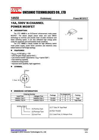
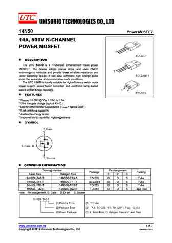
UNISONIC TECHNOLOGIES CO., LTD 14N50 Preliminary Power MOSFET 14A, 500V N-CHANNEL POWER MOSFET DESCRIPTION The UTC 14N50 is an N-Channel enhancement mode power 1 MOSFET. The device adopts planar stripe and uses DMOS technology to minimize and provide lower on-state resistance and TO-263 faster switching speed. It can also withstand high energy pulse under the avalanche and
0.2. Size:178K motorola
mtw14n50e.pdf
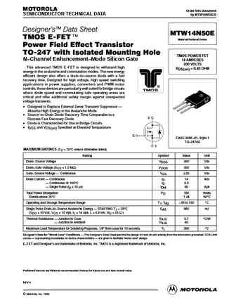
MOTOROLA Order this document SEMICONDUCTOR TECHNICAL DATA by MTW14N50E/D Designer's Data Sheet MTW14N50E TMOS E-FET. Motorola Preferred Device Power Field Effect Transistor TO-247 with Isolated Mounting Hole TMOS POWER FET N Channel Enhancement Mode Silicon Gate 14 AMPERES 500 VOLTS This advanced TMOS E FET is designed to withstand high RDS(on) = 0.40 OHM energy in th
0.3. Size:205K motorola
mtw14n50erev4.pdf

MOTOROLA Order this document SEMICONDUCTOR TECHNICAL DATA by MTW14N50E/D Designer's Data Sheet MTW14N50E TMOS E-FET. Motorola Preferred Device Power Field Effect Transistor TO-247 with Isolated Mounting Hole TMOS POWER FET N Channel Enhancement Mode Silicon Gate 14 AMPERES 500 VOLTS This advanced TMOS E FET is designed to withstand high RDS(on) = 0.40 OHM energy in th
0.4. Size:84K philips
phw14n50e 3.pdf
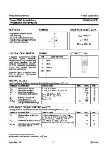
Philips Semiconductors Product specification PowerMOS transistors PHW14N50E Avalanche energy rated FEATURES SYMBOL QUICK REFERENCE DATA d Repetitive Avalanche Rated Fast switching VDSS = 500 V Stable off-state characteristics High thermal cycling performance ID = 14 A g Low thermal resistance RDS(ON) 0.4 s GENERAL DESCRIPTION PINNING SOT429 (TO247) N
0.6. Size:178K vishay
sihg14n50d.pdf
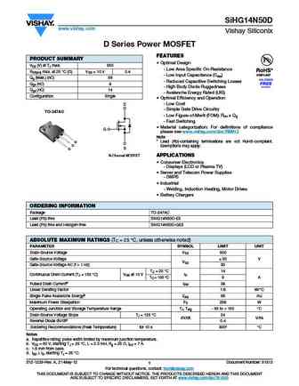
SiHG14N50D www.vishay.com Vishay Siliconix D Series Power MOSFET FEATURES PRODUCT SUMMARY Optimal Design VDS (V) at TJ max. 550 - Low Area Specific On-Resistance RDS(on) max. at 25 C ( ) VGS = 10 V 0.4 - Low Input Capacitance (Ciss) Qg (Max.) (nC) 58 - Reduced Capacitive Switching Losses Qgs (nC) 8 - High Body Diode Ruggedness Qgd (nC) 14 - Avalanche Energy Rated (UIS)
0.7. Size:208K vishay
sihp14n50d.pdf
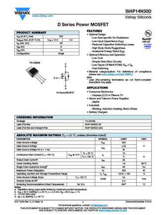
SiHP14N50D www.vishay.com Vishay Siliconix D Series Power MOSFET FEATURES PRODUCT SUMMARY Optimal Design VDS (V) at TJ max. 550 - Low Area specific On-Resistance RDS(on) max. at 25 C ( ) VGS = 10 V 0.4 - Low Input Capacitance (Ciss) Qg max. (nC) 58 - Reduced Capacitive Switching Losses Qgs (nC) 8 - High Body Diode Ruggedness Qgd (nC) 14 - Avalanche Energy Rated (UIS) Co
0.8. Size:103K onsemi
mtw14n50e.pdf
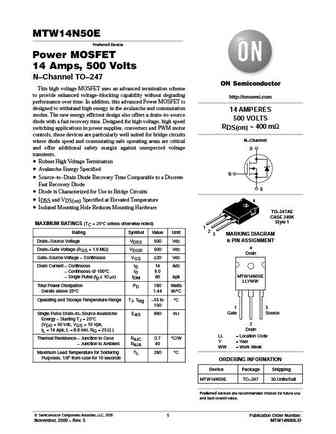
MTW14N50E Preferred Device Power MOSFET 14 Amps, 500 Volts N Channel TO 247 This high voltage MOSFET uses an advanced termination scheme to provide enhanced voltage blocking capability without degrading http //onsemi.com performance over time. In addition, this advanced Power MOSFET is designed to withstand high energy in the avalanche and commutation 14 AMPERES modes. The new
0.9. Size:410K utc
14n50l-tf1-t 14n50g-tf1-t 14n50l-tf3-t 14n50g-tf3-t 14n50l-t3p-t 14n50g-t3p-t.pdf
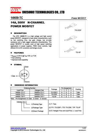
UNISONIC TECHNOLOGIES CO., LTD 14N50-TC Power MOSFET 14A, 500V N-CHANNEL POWER MOSFET 1 TO-220F DESCRIPTION The UTC 14N50-TC is a high voltage and high current power MOSFET, designed to have better characteristics, such as fast switching time, low gate charge, low on-state 1 TO-220F1 resistance and a high rugged avalanche characteristics. This power MOSFET is usually u
0.11. Size:324K aosemi
aowf14n50.pdf
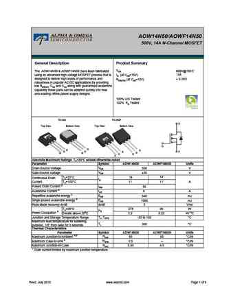
AOW14N50/AOWF14N50 500V, 14A N-Channel MOSFET General Description Product Summary VDS The AOW14N50 & AOWF14N50 have been fabricated 600V@150 using an advanced high voltage MOSFET process that is 14A ID (at VGS=10V) designed to deliver high levels of performance and
0.12. Size:258K aosemi
aob14n50.pdf
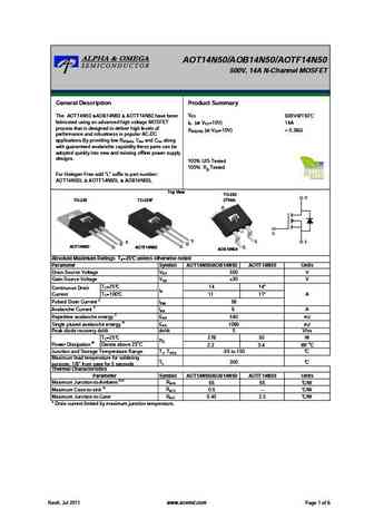
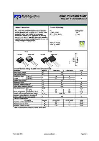
AOT14N50/AOB14N50/AOTF14N50 500V, 14A N-Channel MOSFET General Description Product Summary VDS 600V@150 The AOT14N50 &AOB14N50 & AOTF14N50 have been fabricated using an advanced high voltage MOSFET ID (at VGS=10V) 14A process that is designed to deliver high levels of RDS(ON) (at VGS=10V)
0.13. Size:258K aosemi
aot14n50.pdf

AOT14N50/AOB14N50/AOTF14N50 500V, 14A N-Channel MOSFET General Description Product Summary VDS 600V@150 The AOT14N50 &AOB14N50 & AOTF14N50 have been fabricated using an advanced high voltage MOSFET ID (at VGS=10V) 14A process that is designed to deliver high levels of RDS(ON) (at VGS=10V)
0.14. Size:232K aosemi
aotf14n50fd.pdf

AOT14N50FD/AOTF14N50FD 500V, 14A N-Channel MOSFET General Description Product Summary VDS 600V@150 The AOT14N50FD/AOTF14N50FD have been fabricated using an advanced high voltage MOSFET process that is ID (at VGS=10V) 14A designed to deliver high levels of performance and RDS(ON) (at VGS=10V)
0.15. Size:232K aosemi
aot14n50fd.pdf
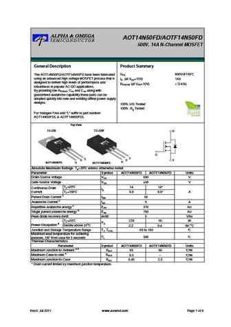
AOT14N50FD/AOTF14N50FD 500V, 14A N-Channel MOSFET General Description Product Summary VDS 600V@150 The AOT14N50FD/AOTF14N50FD have been fabricated using an advanced high voltage MOSFET process that is ID (at VGS=10V) 14A designed to deliver high levels of performance and RDS(ON) (at VGS=10V)
0.16. Size:258K aosemi
aotf14n50.pdf

AOT14N50/AOB14N50/AOTF14N50 500V, 14A N-Channel MOSFET General Description Product Summary VDS 600V@150 The AOT14N50 &AOB14N50 & AOTF14N50 have been fabricated using an advanced high voltage MOSFET ID (at VGS=10V) 14A process that is designed to deliver high levels of RDS(ON) (at VGS=10V)
0.17. Size:180K aosemi
aot14n50 aotf14n50.pdf
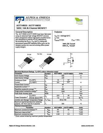
AOT14N50 / AOTF14N50 500V, 14A N-Channel MOSFET General Description Features The AOT14N50 & AOTF14N50 have been fabricated using an advanced high voltage MOSFET process VDS (V) = 600V@150 C that is designed to deliver high levels of performance ID=14A and robustness in popular AC-DC applications. RDS(ON)
0.18. Size:285K aosemi
aow14n50 aowf14n50.pdf
AOW14N50/AOWF14N50 500V, 14A N-Channel MOSFET General Description Product Summary VDS 600V@150 The AOW14N50 & AOWF14N50 have been fabricated using an advanced high voltage MOSFET process that is ID (at VGS=10V) 14A designed to deliver high levels of performance and RDS(ON) (at VGS=10V)
0.19. Size:323K aosemi
aow14n50.pdf

AOW14N50/AOWF14N50 500V, 14A N-Channel MOSFET General Description Product Summary VDS The AOW14N50 & AOWF14N50 have been fabricated 600V@150 using an advanced high voltage MOSFET process that is 14A ID (at VGS=10V) designed to deliver high levels of performance and
0.20. Size:123K inpower semi
fta14n50c ftp14n50c.pdf
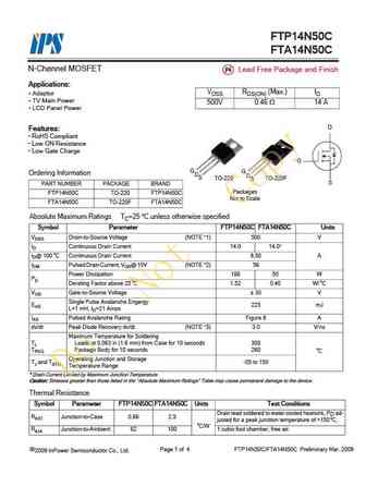
FTP14N50C FTA14N50C N-Channel MOSFET Pb Lead Free Package and Finish Applications VDSS RDS(ON) (Max.) ID Adaptor TV Main Power 500V 0.46 14 A LCD Panel Power D Features RoHS Compliant Low ON Resistance Low Gate Charge G G G Ordering Information DS DS TO-220F TO-220 S PART NUMBER PACKAGE BRAND Packages FTP14N50C TO-220 FTP14N50C Not to Sc
0.21. Size:190K champion
cmt14n50.pdf
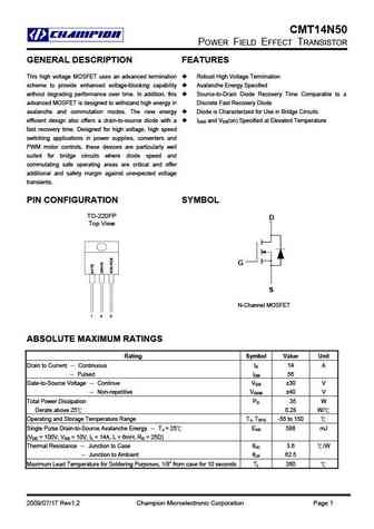
CMT14N50 POWER FIELD EFFECT TRANSISTOR GENERAL DESCRIPTION FEATURES This high voltage MOSFET uses an advanced termination Robust High Voltage Termination scheme to provide enhanced voltage-blocking capability Avalanche Energy Specified without degrading performance over time. In addition, this Source-to-Drain Diode Recovery Time Comparable to a advanced MOSFET is designed to w
0.22. Size:229K crownpo
ctm14n50.pdf
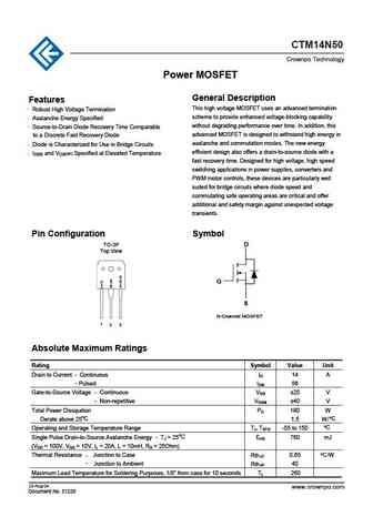
CTM14N50 Crownpo Technology Power MOSFET General Description Features . This high voltage MOSFET uses an advanced termination Robust High Voltage Termination . scheme to provide enhanced voltage-blocking capability Avalanche Energy Specified . without degrading performance over time. In addition, this Source-to-Drain Diode Recovery Time Comparable advanced MOSFET is designed to wit
0.23. Size:819K samwin
swf14n50d.pdf
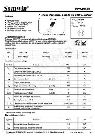
SW14N50D N-channel Enhanced mode TO-220F MOSFET Features TO-220F BVDSS 500V High ruggedness Low RDS(ON) (Typ 0.38 )@VGS=10V ID 14A Low Gate Charge (Typ 54nC) RDS(ON) 0.38 Improved dv/dt Capability 100% Avalanche Tested 2 1 Application Charger, Adaptor, LED 2 3 1 1. Gate 2. Drain 3. Source General Description 3 This power MOSFET is produce
0.24. Size:4922K first semi
fir14n50fg.pdf
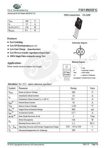
FIR14N50FG CREAT BY ART Advanced N-Ch Power MOSFET-G PIN Connection TO-220F VDSS 500 V ID 13 A PD (TC=25 ) 150 W RDS(ON) 0.4 G D S Features Fast Switching g Schematic dia ram Low ON Resistance(Rdson 0.5 ) D Low Gate Charge (Typical Data 85nC) Low Reverse transfer capacitances(Typical 100pF) G 100% Single Pulse avalanche energy Test S Marking Di
0.25. Size:253K inchange semiconductor
aob14n50.pdf
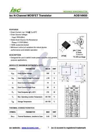
isc N-Channel MOSFET Transistor AOB14N50 FEATURES Drain Current I = 14A@ T =25 D C Drain Source Voltage- V = 500V(Min) DSS Static Drain-Source On-Resistance R = 0.38 (Max) DS(on) 100% avalanche tested Minimum Lot-to-Lot variations for robust device performance and reliable operation DESCRIPTION Designed for use in switch mode power supplies and general purp
0.26. Size:260K inchange semiconductor
aot14n50.pdf
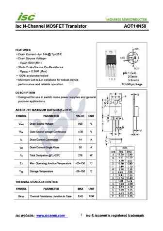
isc N-Channel MOSFET Transistor AOT14N50 FEATURES Drain Current I = 14A@ T =25 D C Drain Source Voltage- V = 500V(Min) DSS Static Drain-Source On-Resistance R = 0.38 (Max) DS(on) 100% avalanche tested Minimum Lot-to-Lot variations for robust device performance and reliable operation DESCRIPTION Designed for use in switch mode power supplies and general purp
0.27. Size:250K inchange semiconductor
aotf14n50fd.pdf
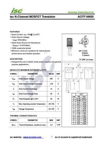
isc N-Channel MOSFET Transistor AOTF14N50FD FEATURES Drain Current I = 14A@ T =25 D C Drain Source Voltage- V = 500V(Min) DSS Static Drain-Source On-Resistance R = 0.47 (Max) DS(on) 100% avalanche tested Minimum Lot-to-Lot variations for robust device performance and reliable operation DESCRIPTION Designed for use in switch mode power supplies and general p
0.28. Size:260K inchange semiconductor
aot14n50fd.pdf

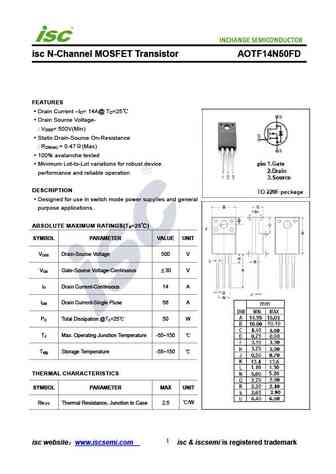
isc N-Channel MOSFET Transistor AOT14N50FD FEATURES Drain Current I = 14A@ T =25 D C Drain Source Voltage- V = 500V(Min) DSS Static Drain-Source On-Resistance R = 0.47 (Max) DS(on) 100% avalanche tested Minimum Lot-to-Lot variations for robust device performance and reliable operation DESCRIPTION Designed for use in switch mode power supplies and general pu
0.29. Size:250K inchange semiconductor
aotf14n50.pdf
isc N-Channel MOSFET Transistor AOTF14N50 FEATURES Drain Current I = 14A@ T =25 D C Drain Source Voltage- V = 500V(Min) DSS Static Drain-Source On-Resistance R = 0.38 (Max) DS(on) 100% avalanche tested Minimum Lot-to-Lot variations for robust device performance and reliable operation DESCRIPTION Designed for use in switch mode power supplies and general pur
0.30. Size:298K inchange semiconductor
aow14n50.pdf
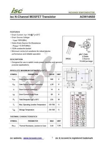
isc N-Channel MOSFET Transistor AOW14N50 FEATURES Drain Current I = 14A@ T =25 D C Drain Source Voltage- V = 500V(Min) DSS Static Drain-Source On-Resistance R = 0.38 (Max) DS(on) 100% avalanche tested Minimum Lot-to-Lot variations for robust device performance and reliable operation DESCRIPTION Designed for use in switch mode power supplies and general purp
Otros transistores... 4N60Z, 4N60K, 8N50H, 9N50, 10N50, 11N50, 12N50, 13N50, IRFB4115, 15N50, 16N50, 18N50, 24N50, 26N50, UF830, UF830Z, UF840