18N50 Datasheet. Equivalente. Reemplazo. Hoja de especificaciones. Principales características
Número de Parte: 18N50 📄📄
Tipo de FET: MOSFET
Polaridad de transistor: N
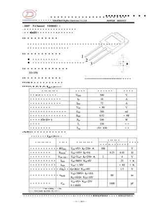
ESPECIFICACIONES MÁXIMAS
Pdⓘ - Máxima disipación de potencia: 277 W
|Vds|ⓘ - Voltaje máximo drenador-fuente: 500 V
|Vgs|ⓘ - Voltaje máximo fuente-puerta: 30 V
|Id|ⓘ - Corriente continua de drenaje: 18 A
Tjⓘ - Temperatura máxima de unión: 150 °C
CARACTERÍSTICAS ELÉCTRICAS
trⓘ - Tiempo de subida: 165 nS
Cossⓘ - Capacitancia de salida: 330 pF
RDSonⓘ - Resistencia estado encendido drenaje a fuente: 0.24 Ohm
📄📄 Copiar
Búsqueda de reemplazo de 18N50 MOSFET
- Selecciónⓘ de transistores por parámetros
18N50 datasheet
18n50.pdf

UNISONIC TECHNOLOGIES CO., LTD 18N50 Power MOSFET 18A, 500V N-CHANNEL POWER MOSFET 1 1 TO-230 TO-220F1 DESCRIPTION The UTC 18N50 is an N-channel enhancement mode power MOSFET using UTC s advanced planar stripe and DMOS technology to provide perfect performance. This technology can withstand high energy pulse in the avalanche and commutation mode. It can provide minimum
18n50.pdf
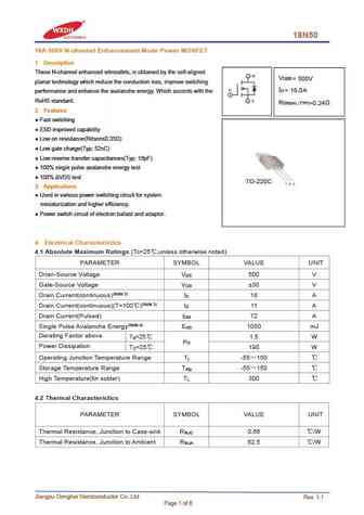
18N50 18A 500V N-channel Enhancement Mode Power MOSFET 1 Description These N-channel enhanced vdmosfets, is obtained by the self-aligned V DSS = 500V planar technology which reduce the conduction loss, improve switching I = 18.0A D performance and enhance the avalanche energy. Which accords with the RoHS standard. R DS(on) TYP) =0.24 2 Features Fast switching ESD imp
gpt18n50g gpt18n50dg.pdf
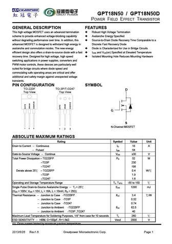
GPT18N50 / GPT18N50D POWER FIELD EFFECT TRANSISTOR Fig 5. Typical Capacitance Vs. Fig 6. Typical Gate Charge Vs. Drain-to-Source Voltage Gate-to-Source Voltage 2013/6/26 Rev1.6 Greatpower Microelectronic Corp. Page 4 GPT18N50 / GPT18N50D POWER FIELD EFFECT TRANSISTOR PACKAGE DIMENSION TO-220F 2013/6/26 Rev1.6 Greatpower Microelectronic Corp. Page 5 GPT18N50 / GPT18N50D
fqp18n50v2 fqpf18n50v2.pdf
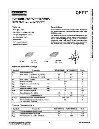
QFET FQP18N50V2/FQPF18N50V2 500V N-Channel MOSFET Features Description 550V @TJ = 150 C These N-Channel enhancement mode power field effect transis- tors are produced using Fairchild s proprietary, planar stripe, Typ. RDS(on) = 0.265 @VGS = 10 V DMOS technology. Low gate charge (typical 42 nC) This advanced technology has been especially tailored to mini- Lo
mtu18n50erev1.pdf
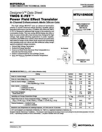
MOTOROLA Order this document SEMICONDUCTOR TECHNICAL DATA by MTU18N50E/D Designer's Data Sheet MTU18N50E TMOS E-FET. Power Field Effect Transistor N Channel Enhancement Mode Silicon Gate TMOS POWER FET This high voltage MOSFET uses an advanced termination 18 AMPERES scheme to provide enhanced voltage blocking capability without 500 VOLTS degrading performance over time
mtu18n50e.pdf

MOTOROLA Order this document SEMICONDUCTOR TECHNICAL DATA by MTU18N50E/D Designer's Data Sheet MTU18N50E TMOS E-FET. Power Field Effect Transistor N Channel Enhancement Mode Silicon Gate TMOS POWER FET This high voltage MOSFET uses an advanced termination 18 AMPERES scheme to provide enhanced voltage blocking capability without 500 VOLTS degrading performance over time
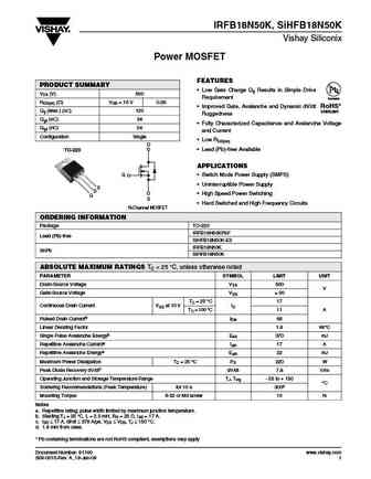
irfb18n50k.pdf
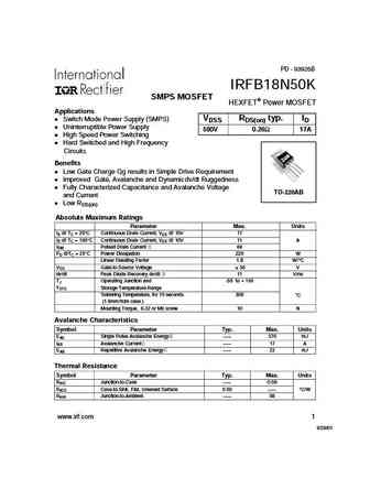
PD - 93926B IRFB18N50K SMPS MOSFET HEXFET Power MOSFET Applications VDSS RDS(on) typ. ID Switch Mode Power Supply (SMPS) Uninterruptible Power Supply 500V 0.26 17A High Speed Power Switching Hard Switched and High Frequency Circuits Benefits Low Gate Charge Qg results in Simple Drive Requirement Improved Gate, Avalanche and Dynamicdv/dt Ruggedness Fully Characterized
irfbl18n50k.pdf
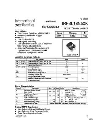
PD- 93928 PROVISIONAL IRFBL18N50K SMPS MOSFET HEXFET Power MOSFET Applications VDSS RDS(on) ID Telecom and Data-Com off-Line SMPS UninterruptIble Power Supply 500V 0.25 18A Benefits Low On-Resistance High Speed Switching Low Gate Drive Current Due to Improved Gate Charge Characteristics Improved Avalanche Ruggedness and Dynamic dv/dt, Fully Characterized Avalanche Vo
irfb18n50kpbf.pdf
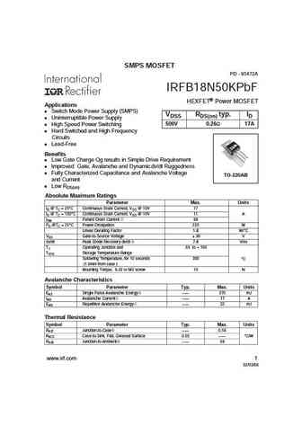
SMPS MOSFET PD - 95472A IRFB18N50KPbF HEXFET Power MOSFET Applications l Switch Mode Power Supply (SMPS) VDSS RDS(on) typ. ID l Uninterruptible Power Supply 500V 0.26 17A l High Speed Power Switching l Hard Switched and High Frequency Circuits l Lead-Free Benefits l Low Gate Charge Qg results in Simple Drive Requirement l Improved Gate, Avalanche and Dynamicdv/dt Ruggedness
fdp18n50 fdpf18n50 fdpf18n50t.pdf
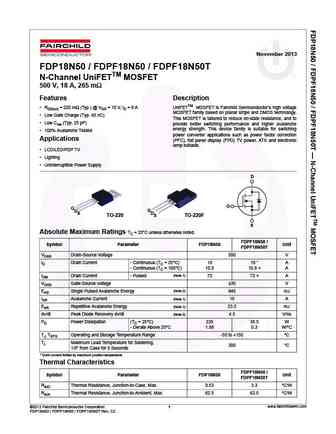
November 2013 FDP18N50 / FDPF18N50 / FDPF18N50T N-Channel UniFETTM MOSFET 500 V, 18 A, 265 m Features Description RDS(on) = 220 m (Typ.) @ VGS = 10 V, ID = 9 A UniFETTM MOSFET is Fairchild Semiconductor s high voltage MOSFET family based on planar stripe and DMOS technology. Low Gate Charge (Typ. 45 nC) This MOSFET is tailored to reduce on-state resistance, and to Low
fdp18n50 fdpf18n50.pdf
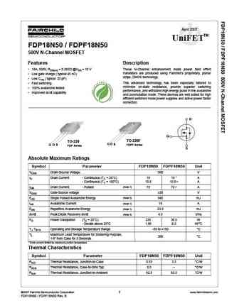
April 2007 TM UniFET FDP18N50 / FDPF18N50 500V N-Channel MOSFET Features Description 18A, 500V, RDS(on) = 0.265 @VGS = 10 V These N-Channel enhancement mode power field effect transistors are produced using Fairchild s proprietary, planar Low gate charge ( typical 45 nC) stripe, DMOS technology. Low Crss ( typical 25 pF) This advanced technology has been especially
fqh18n50v2.pdf
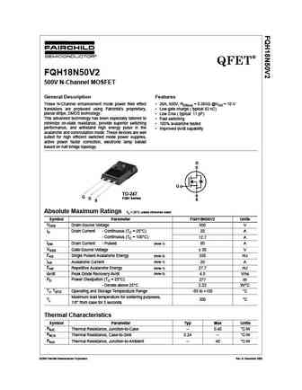
QFET FQH18N50V2 500V N-Channel MOSFET General Description Features These N-Channel enhancement mode power field effect 20A, 500V, RDS(on) = 0.265 @VGS = 10 V transistors are produced using Fairchild s proprietary, Low gate charge ( typical 42 nC) planar stripe, DMOS technology. Low Crss ( typical 11 pF) This advanced technology has been especially tailored to F
fda18n50.pdf
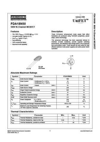
October 2006 TM UniFET FDA18N50 500V N-Channel MOSFET Features Description 19A, 500V, RDS(on) = 0.265 @VGS = 10 V These N-Channel enhancement mode power field effect transistors are produced using Fairchild s proprietary, planar Low gate charge ( typical 45 nC) stripe, DMOS technology. Low Crss ( typical 25 pF) This advanced technology has been especially tailored to
fqpf18n50v2.pdf
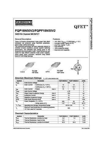
TM QFET FQP18N50V2/FQPF18N50V2 500V N-Channel MOSFET General Description Features These N-Channel enhancement mode power field effect 18A, 500V, RDS(on) = 0.265 @VGS = 10 V transistors are produced using Fairchild s proprietary, Low gate charge ( typical 42 nC) planar stripe, DMOS technology. Low Crss ( typical 11 pF) This advanced technology has been especially tailor
fqa18n50v2.pdf
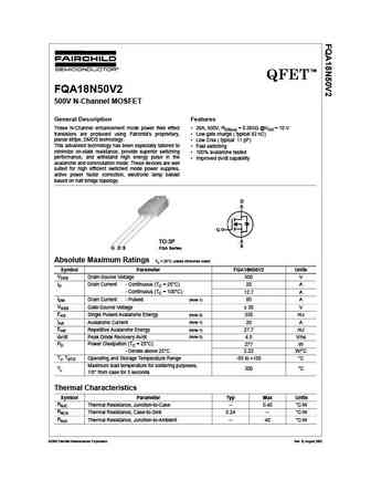
TM QFET FQA18N50V2 500V N-Channel MOSFET General Description Features These N-Channel enhancement mode power field effect 20A, 500V, RDS(on) = 0.265 @VGS = 10 V transistors are produced using Fairchild s proprietary, Low gate charge ( typical 42 nC) planar stripe, DMOS technology. Low Crss ( typical 11 pF) This advanced technology has been especially tailored to F
fqp18n50v2.pdf
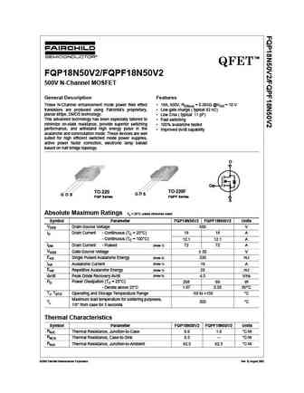
TM QFET FQP18N50V2/FQPF18N50V2 500V N-Channel MOSFET General Description Features These N-Channel enhancement mode power field effect 18A, 500V, RDS(on) = 0.265 @VGS = 10 V transistors are produced using Fairchild s proprietary, Low gate charge ( typical 42 nC) planar stripe, DMOS technology. Low Crss ( typical 11 pF) This advanced technology has been especially tailor
irfb18n50k.pdf
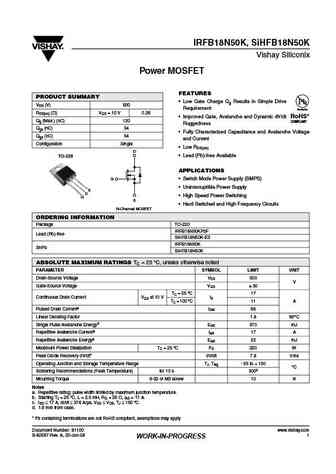
IRFB18N50K, SiHFB18N50K Vishay Siliconix Power MOSFET FEATURES PRODUCT SUMMARY Low Gate Charge Qg Results in Simple Drive VDS (V) 500 Requirement Available RDS(on) ( )VGS = 10 V 0.26 Improved Gate, Avalanche and Dynamic dV/dt RoHS* Qg (Max.) (nC) 120 COMPLIANT Ruggedness Qgs (nC) 34 Fully Characterized Capacitance and Avalanche Voltage Qgd (nC) 54 and Current Con
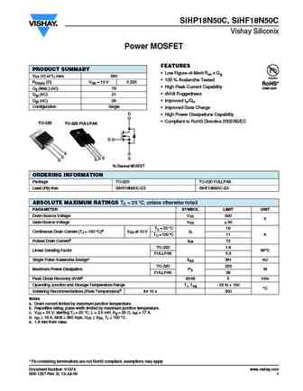
sihp18n50c.pdf
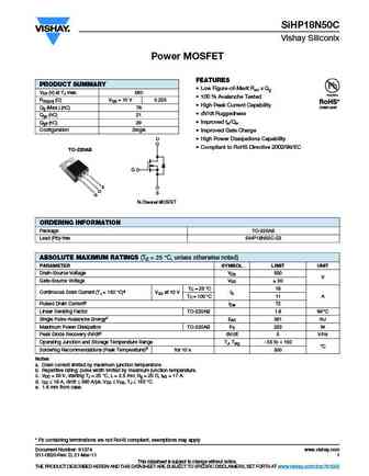
SiHP18N50C Vishay Siliconix Power MOSFET FEATURES PRODUCT SUMMARY Low Figure-of-Merit Ron x Qg VDS (V) at TJ max. 560 100 % Avalanche Tested RDS(on) ( )VGS = 10 V 0.225 High Peak Current Capability Qg (Max.) (nC) 76 dV/dt Ruggedness Qgs (nC) 21 Qgd (nC) 29 Improved trr/Qrr Configuration Single Improved Gate Charge D High Power Dissipations Capabilit
sihf18n50c.pdf
SiHP18N50C, SiHF18N50C Vishay Siliconix Power MOSFET FEATURES PRODUCT SUMMARY Low Figure-of-Merit Ron x Qg VDS (V) at TJ max. 560 100 % Avalanche Tested RDS(on) ( )VGS = 10 V 0.225 High Peak Current Capability Qg (Max.) (nC) 76 dV/dt Ruggedness Qgs (nC) 21 Qgd (nC) 29 Improved trr/Qrr Configuration Single Improved Gate Charge D High Power Dissipati
sihf18n50d.pdf
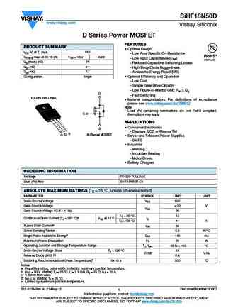
SiHF18N50D www.vishay.com Vishay Siliconix D Series Power MOSFET FEATURES PRODUCT SUMMARY Optimal Design VDS (V) at TJ max. 550 - Low Area Specific On-Resistance RDS(on) max. at 25 C ( ) VGS = 10 V 0.28 - Low Input Capacitance (Ciss) Qg (max.) (nC) 76 - Reduced Capacitive Switching Losses Qgs (nC) 11 - High Body Diode Ruggedness Qgd (nC) 17 - Avalanche Energy Rated (UIS)
irfb18n50k sihfb18n50k.pdf
IRFB18N50K, SiHFB18N50K Vishay Siliconix Power MOSFET FEATURES PRODUCT SUMMARY Low Gate Charge Qg Results in Simple Drive VDS (V) 500 Requirement Available RDS(on) ( )VGS = 10 V 0.26 Improved Gate, Avalanche and Dynamic dV/dt RoHS* Qg (Max.) (nC) 120 COMPLIANT Ruggedness Qgs (nC) 34 Fully Characterized Capacitance and Avalanche Voltage Qgd (nC) 54 and Current Con
ixz4df18n50.pdf
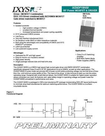
IXZ4DF18N50 RF Power MOSFET & DRIVER 500 Volts Driver / MOSFET Combination 19 A DEIC-515 Driver combined with IXZ318N50 MOSFET 0.29 Ohms Gate driver matched to MOSFET Features Isolated substrate - high isolation voltage (>2500V) - excellent thermal transfer - Increased temperature and power cycling capability IXYS advanced Z-MOS process Low Rds(ON)
ixz318n50.pdf
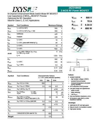
IXZ318N50 Z-MOS RF Power MOSFET N-Channel Enhancement Mode Switch Mode RF MOSFET Low Capacitance Z-MOSTM MOSFET Process VDSS = 500 V Optimized for RF Operation Ideal for Class C, D, & E Applications ID25 = 19 A RDS(on) Symbol Test Conditions Maximum Ratings 0.34 TJ = 25 C to 150 C VDSS 500 V PDC = 880 W TJ = 25 C to 150 C; RGS = 1 M VDGR
ixzr18n50a ixzr18n50b.pdf
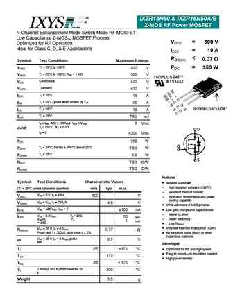
IXZR18N50 & IXZR18N50A/B Z-MOS RF Power MOSFET N-Channel Enhancement Mode Switch Mode RF MOSFET Low Capacitance Z-MOSTM MOSFET Process VDSS = 500 V Optimized for RF Operation Ideal for Class C, D, & E Applications ID25 = 19 A RDS(on) 0.37 Symbol Test Conditions Maximum Ratings TJ = 25 C to 150 C VDSS 500 V PDC = 350 W TJ = 25 C to 150 C; RGS
fdp18n50 fdpf18n50 fdpf18n50t.pdf
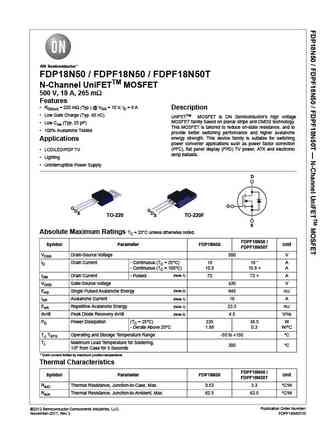
FDP18N50 / FDPF18N50 / FDPF18N50T N-Channel UniFETTM MOSFET 500 V, 18 A, 265 m Features RDS(on) = 220 m (Typ.) @ VGS = 10 V, ID = 9 A Description Low Gate Charge (Typ. 45 nC) UniFETTM MOSFET is ON Semiconductor s high voltage MOSFET family based on planar stripe and DMOS technology. Low Crss (Typ. 25 pF) This MOSFET is tailored to reduce on-state resistance, and to
fdp18n50 fdpf18n50.pdf
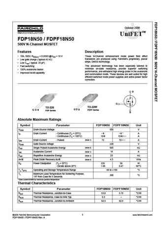
October 2006 TM UniFET FDP18N50 / FDPF18N50 500V N-Channel MOSFET Features Description 18A, 500V, RDS(on) = 0.265 @VGS = 10 V These N-Channel enhancement mode power field effect transistors are produced using Fairchild s proprietary, planar Low gate charge ( typical 45 nC) stripe, DMOS technology. Low Crss ( typical 25 pF) This advanced technology has been especially
fda18n50.pdf

Is Now Part of To learn more about ON Semiconductor, please visit our website at www.onsemi.com Please note As part of the Fairchild Semiconductor integration, some of the Fairchild orderable part numbers will need to change in order to meet ON Semiconductor s system requirements. Since the ON Semiconductor product management systems do not have the ability to manage part nomenclatur
ap18n50w.pdf
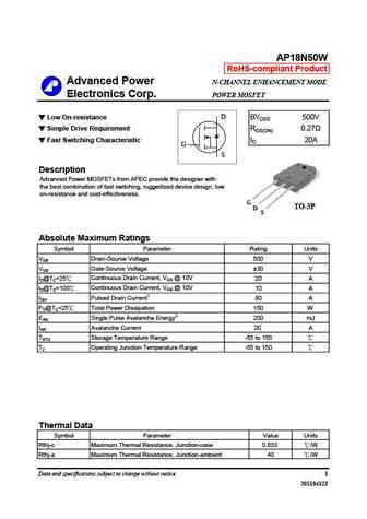
AP18N50W RoHS-compliant Product Advanced Power N-CHANNEL ENHANCEMENT MODE Electronics Corp. POWER MOSFET D Low On-resistance BVDSS 500V Simple Drive Requirement RDS(ON) 0.27 Fast Switching Characteristic ID 20A G S Description Advanced Power MOSFETs from APEC provide the designer with the best combination of fast switching, ruggedized device design, low on-resistance
jcs18n50be jcs18n50se jcs18n50ce jcs18n50fe.pdf
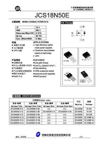
N N- CHANNEL MOSFET R JCS18N50E MAIN CHARACTERISTICS Package ID 18 A VDSS 500 V Rdson-max @Vgs=10V 0.27 Qg-typ 48.7nC Eoss @Vdss=400V 5.84mJ APPLICATIONS High efficiency switch mode power supplies Electronic lamp ballasts UPS
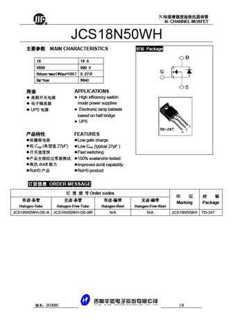
jcs18n50we jcs18n50abe.pdf
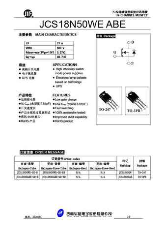
N N- CHANNEL MOSFET R JCS18N50WE ABE MAIN CHARACTERISTICS Package ID 19 A VDSS 500 V Rdson-max @Vgs=10V 0.27 Qg-typ 48.7nC APPLICATIONS High efficiency switch mode power supplies Electronic lamp ballasts UPS based on half bridge
mp18n50eif mp18n50eic.pdf
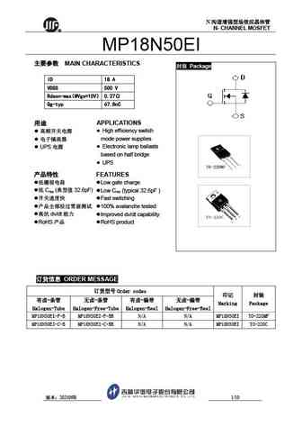
N N- CHANNEL MOSFET R MP18N50EI MAIN CHARACTERISTICS Package ID 18 A VDSS 500 V Rdson-max @Vgs=10V 0.27 Qg-typ 67.8nC APPLICATIONS High efficiency switch mode power supplies Electronic lamp ballasts UPS based on half bridge
18n50a.pdf
GOFORD 18N50A Description Features VDSS RDS(ON) ID @ 10V (typ) 18A 500V 0.22 Fast switching 100% avalanche tested Improved dv/dt capability Application Active power factor correction Uninterruptible Power Supply (UPS) Electronic lamp ballasts Absolute Maximum Ratings TC=25 unless otherwise specified Max. Symbol Parameter Units
sdf18n50 sdp18n50.pdf
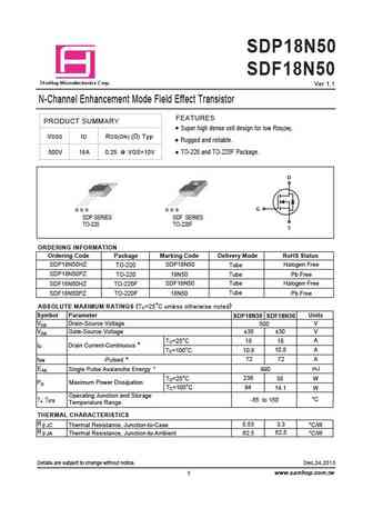
SDP18N50 SDF18N50 a S mHop Microelectronics C orp. Ver 1.1 N-Channel Enhancement Mode Field Effect Transistor FEATURES PRODUCT SUMMARY Super high dense cell design for low RDS(ON). VDSS ID RDS(ON) ( ) Typ Rugged and reliable. 500V 18A 0.25 @ VGS=10V TO-220 and TO-220F Package. D G G D S G D S SDP SERIES SDF SERIES TO-220 TO-220F S ORDERING INFORMATION Ordering Code Package M
ssf18n50f.pdf
SSF18N50F Main Product Characteristics VDSS 500V RDS(on) 0.22ohm(typ.) ID 18A Marking and pin TO220F Schematic diagram Assignment Features and Benefits Advanced Process Technology Special designed for PWM, load switching and general purpose applications Ultra low on-resistance with low gate charge Fast switching and reverse body recovery 150 operating
cm18n50p.pdf
R C1N0 M85P www.jdsemi.cn ShenZhen Jingdao Electronic Co.,Ltd. POWER MOSFET 500V N-Channel VDMOS RoHS 1 2 1 2 3 3
18n50d.pdf
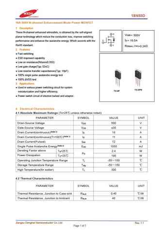
18N50D 18A 500V N-channel Enhancement Mode Power MOSFET 1 Description These N-channel enhanced vdmosfets, is obtained by the self-aligned V DSS = 500V planar technology which reduce the conduction loss, improve switching I = 18.0A D performance and enhance the avalanche energy. Which accords with the RoHS standard. R DS(on) TYP) =0.24 2 Features Fast switching ESD im
f18n50.pdf
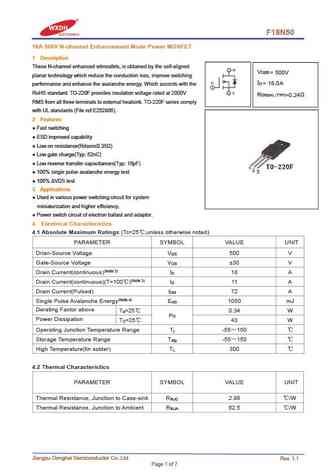
F18N50 18A 500V N-channel Enhancement Mode Power MOSFET 1 Description These N-channel enhanced vdmosfets, is obtained by the self-aligned V DSS = 500V planar technology which reduce the conduction loss, improve switching I = 18.0A D performance and enhance the avalanche energy. Which accords with the RoHS standard. TO-220F provides insulation voltage rated at 2000V R DS(on) TYP)
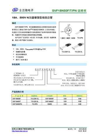
svf18n50f svf18n50t svf18n50pn svf18n50fj.pdf
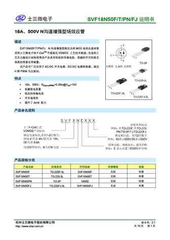
SVF18N50F/T/PN/FJ 18A 500V N SVF18N50F/T/PN/FJ N MOS F-CellTM VDMOS
mdf18n50.pdf
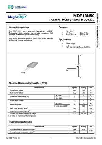
MDF18N50 N-Channel MOSFET 500V, 18 A, 0.27 General Description Features The MDF18N50 uses advanced MagnaChip s MOSFET V = 500V DS Technology, which provides low on-state resistance, high I = 18A @V = 10V D GS R 0.27 @V = 10V switching performance and excellent quality. DS(ON) GS MDF18N50 is suitable device for SMPS, high speed switching Applications and general
mdf18n50bth mdp18n50bth.pdf
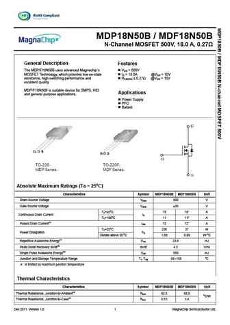
MDP18N50B / MDF18N50B N-Channel MOSFET 500V, 18.0 A, 0.27 General Description Features The MDP/F18N50B uses advanced Magnachip s VDS = 500V MOSFET Technology, which provides low on-state ID = 18.0A @VGS = 10V resistance, high switching performance and RDS(ON) 0.27 @VGS = 10V excellent quality. MDP/F18N50B is suitable device for SMPS, HID Applications and general
mdp18n50th.pdf
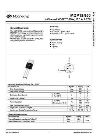
MDP18N50 N-Channel MOSFET 500V, 18.0 A, 0.27 Features General Description V = 500V DS The MDP18N50 uses advanced Magnachip s I = 18.0A @V = 10V D GS MOSFET Technology, which provides low on- R
mdq18n50gth mdq18n50gtp.pdf
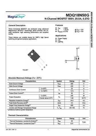
MDQ18N50G N-Channel MOSFET 500V, 20.0A, 0.27 General Description Features . V = 500V DS These N-channel MOSFET are produced using advanced I = 20.0A @ V = 10V D GS MagnaChip s MOSFET Technology, which provides low on- R 0.27 @ V = 10V DS(ON) GS state resistance, high switching performance and excellent quality. Applications These devices are s
ms18n50.pdf
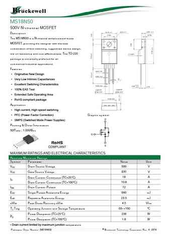
MS18N50 500V N-channel MOSFET Description The MS18N50 is a N-channel enhancement-mode MOSFET, providing the designer with the best combination of fast switching, ruggedized device design, low on-resistance and cost effectiveness. The TO-220 package is universally preferred for all commercial-industrial applications Features Originative New Design Very Low Intrinsic
msf18n50.pdf
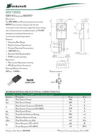
MSF18N50 500V N-Channel MOSFET Description The MSF18N50 is a N-channel enhancement-mode MOSFET, providing the designer with the best combination of fast switching, ruggedized device design, low on-resistance and cost effectiveness. he TO-220F package is universally preferred for all commercial-industrial applications Features Originative New Design Very Low Intrins
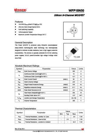
wff18n50.pdf
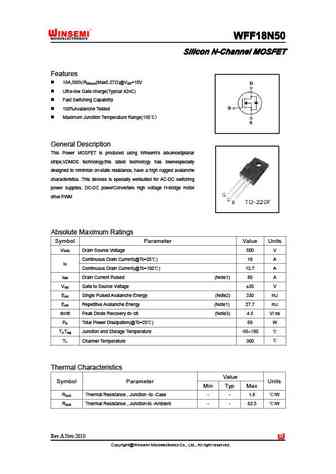
WFF18N50 WFF18N50 WFF18N50 WFF18N50 Silicon N-Channel MOSFET Silicon N-Channel MOSFET Silicon N-Channel MOSFET Silicon N-Channel MOSFET Features 18A,500V,R (Max0.27 )@V =10V DS(on) GS Ultra-low Gate charge(Typical 42nC) Fast Switching Capability 100%Avalanche Tested Maximum Junction Temperature Range(150 ) General Description This Power MOSFET is produced
wfw18n50.pdf
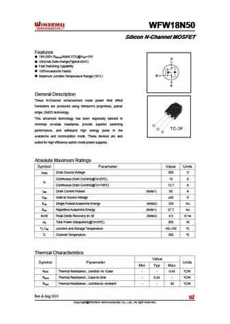
WFW18N50 WFW18N50 WFW18N50 WFW18N50 Silicon N-Channel MOSFET Silicon N-Channel MOSFET Silicon N-Channel MOSFET Silicon N-Channel MOSFET Features 18A,500V,R (Max0.27 )@V =10V DS(on) GS Ultra-low Gate charge(Typical 42nC) Fast Switching Capability 100%Avalanche Tested Maximum Junction Temperature Range(150 ) General Description These N-Channel enhancement
wfw18n50n.pdf
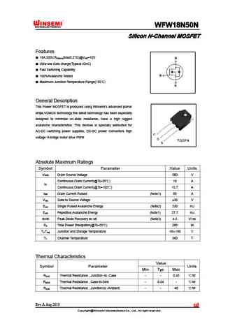
WFW18N50N WFW18N50N WFW18N50N WFW18N50N Silicon N-Channel MOSFET Silicon N-Channel MOSFET Silicon N-Channel MOSFET Silicon N-Channel MOSFET Features 18A,500V,R (Max0.27 )@V =10V DS(on) GS Ultra-low Gate charge(Typical 42nC) Fast Switching Capability 100%Avalanche Tested Maximum Junction Temperature Range(150 ) General Description This Power MOSFET is prod
wfw18n50w.pdf
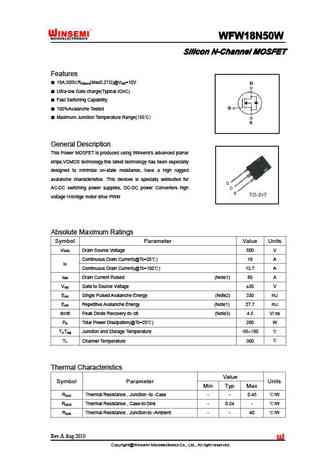
WFW18N50W WFW18N50W WFW18N50W WFW18N50W Silicon N-Channel MOSFET Silicon N-Channel MOSFET Silicon N-Channel MOSFET Silicon N-Channel MOSFET Features 18A,500V,R (Max0.27 )@V =10V DS(on) GS Ultra-low Gate charge(Typical 42nC) Fast Switching Capability 100%Avalanche Tested Maximum Junction Temperature Range(150 ) General Description This Power MOSFET is prod
wfp18n50.pdf
WFP18N50 WFP18N50 WFP18N50 WFP18N50 Silicon N-Channel MOSFET Silicon N-Channel MOSFET Silicon N-Channel MOSFET Silicon N-Channel MOSFET Features 18A,500V,R (Max0.27 )@V =10V DS(on) GS Ultra-low Gate charge(Typical 42nC) Fast Switching Capability 100%Avalanche Tested Maximum Junction Temperature Range(150 ) General Description This Power MOSFET is produced
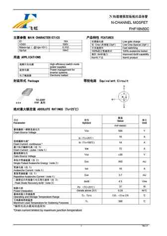
fhf18n50a.pdf

N N-CHANNEL MOSFET FHF18N50A MAIN CHARACTERISTICS FEATURES ID 18A Low gate charge VDSS 500V Crss ( 23pF) Low Crss (typical 23pF ) Rdson-typ @Vgs=10V 0.31 Fast switching Qg-typ 58nC 100% 100% avalanche tested dv/dt Improved dv/d
fhf18n50c.pdf
N N-CHANNEL MOSFET FHF18N50C MAIN CHARACTERISTICS FEATURES ID 18A Low gate charge VDSS 500V Crss ( 23pF) Low Crss (typical 23pF ) Rdson-typ @Vgs=10V 0.31 Fast switching Qg-typ 58nC 100% 100% avalanche tested dv/dt Improved dv/d
hy18n50w.pdf
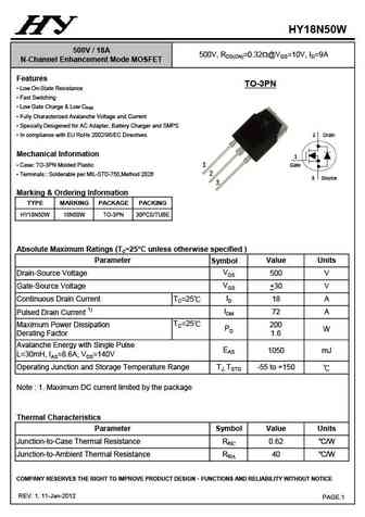
SINGLE FIG.SINGLE PHASE HALF WAVE 60Hz DERATING CURVE FIG. 2 MAXIMUM NON- T1 FORWARD CURRENT AMBIENT TEMPERATURE ( ) 1 2 5 10 1 25 50 75 10 20 150 175 0.00 0.2 0.4 0.6 4 100 125 100 HY18N50W 500V / 18A 500V, RDS(ON)=0.32W@VGS=10V, ID=9A N-Channel Enhancement Mode MOSFET Features TO-3PN Low On-State Resistance Fast Switching Low Gate Charge & Low CR
jfpc18n50c jffm18n50c.pdf
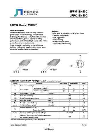
JFFM18N50C JFPC18N50C 500V N-Channel MOSFET General Description Features This Power MOSFET is produced using advanced - 18A, 500V, RDS(on)typ. = 0.24 @VGS = 10 V planar stripe DMOS technology. This advanced - Low gate charge(40nC) technology has been especially tailored to minimize - High ruggedness on-state resistance, provide superior switching - Fast switching perf
jfam18n50c.pdf
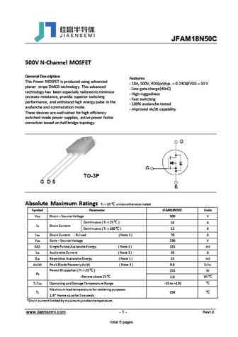
JFAM18N50C 500V N-Channel MOSFET General Description Features This Power MOSFET is produced using advanced - 18A, 500V, RDS(on)typ. = 0.24 @VGS = 10 V planar stripe DMOS technology. This advanced - Low gate charge(40nC) technology has been especially tailored to minimize - High ruggedness on-state resistance, provide superior switching - Fast switching performance, and
kia18n50h.pdf
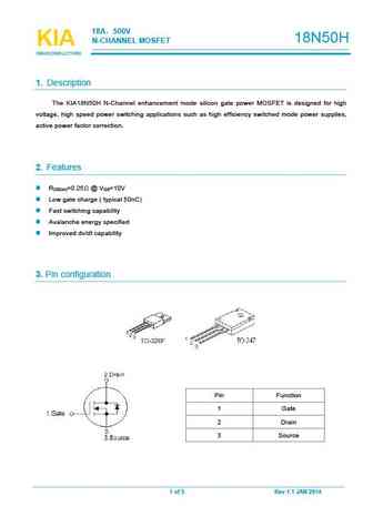
18A 500V 18N50H N-CHANNELMOSFET KIA KIA KIA SEMICONDUCTORS SEMICONDUCTORS SEMICONDUCTORS 1. Description The KIA18N50H N-Channel enhancement mode silicon gate power MOSFET is designed for high voltage, high speed power switching applications such as high efficiency switched mode power supplies, active power factor correction. 2. Features R =0.25 @V =10V DS(on) GS Lowgate c
slw18n50c.pdf
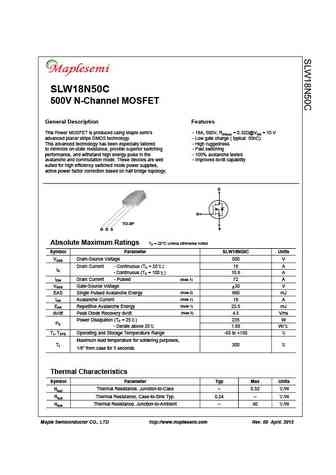
SLW18N50C 500V N-Channel MOSFET General Description Features This Power MOSFET is produced using Msemitek s advanced planar - 18A, 500V, RDS(on)typ = 212m stripe DMOS technology. This advanced technology has been - Low gate charge especially tailored to minimize conduction loss, provide superior - Low Crss - Fast switching switching performance, and withstand high energy pulse in
slp18n50c slf18n50c.pdf
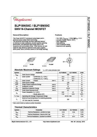
SLP18N50C / SLF18N50C 500V N-Channel MOSFET General Description Features This Power MOSFET is produced using Maple semi s - 18A, 500V, RDS(on)typ. = 236m @VGS = 10 V advanced planar stripe DMOS technology. - Low gate charge ( typical 69nC) This advanced technology has been especially tailored - High ruggedness to minimize on-state resistance, provide superior switching - Fast switching
swf18n50d swt18n50d.pdf

SW18N50D N-channel Enhanced mode TO-220F /TO-247 MOSFET TO-220F TO-247 BVDSS 500V Features ID 18A High ruggedness RDS(ON) 0.24 Low RDS(ON) (Typ 0.24 )@VGS=10V Low Gate Charge (Typ 88nC) 2 Improved dv/dt Capability 1 1 100% Avalanche Tested 2 2 1 3 3 Application LED , Charger, PC Power 1. Gate 2. Drain 3. Source 3 General
sw18n50d swf18n50d swt18n50d.pdf
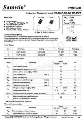
SW18N50D N-channel Enhanced mode TO-220F /TO-247 MOSFET TO-220F TO-247 BVDSS 500V Features ID 18A High ruggedness RDS(ON) 0.24 Low RDS(ON) (Typ 0.24 )@VGS=10V Low Gate Charge (Typ 88nC) 2 Improved dv/dt Capability 1 1 100% Avalanche Tested 2 2 1 3 3 Application LED , Charge, PC Power 1. Gate 2. Drain 3. Source 3 General D
hfs18n50u.pdf
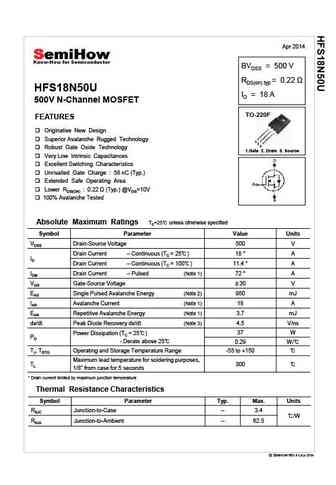
Apr 2014 BVDSS = 500 V RDS(on) typ = 0.22 HFS18N50U ID = 18 A 500V N-Channel MOSFET TO-220F FEATURES Originative New Design Superior Avalanche Rugged Technology 1 2 3 Robust Gate Oxide Technology 1.Gate 2. Drain 3. Source Very Low Intrinsic Capacitances Excellent Switching Characteristics Unrivalled Gate Charge 58 nC (Typ.) Extended Safe Operating Area L
hfs18n50ut.pdf
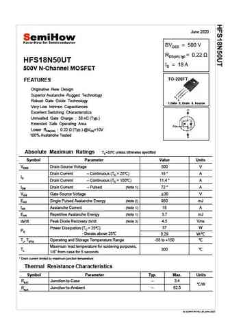
June 2020 BVDSS = 500 V RDS(on) typ = 0.22 HFS18N50UT ID = 18 A 500V N-Channel MOSFET TO-220FT FEATURES Originative New Design Superior Avalanche Rugged Technology 1 2 3 Robust Gate Oxide Technology 1.Gate 2. Drain 3. Source Very Low Intrinsic Capacitances Excellent Switching Characteristics Unrivalled Gate Charge 58 nC (Typ.) Extended Safe Operating Area Lower RDS(ON)
hfp18n50u.pdf
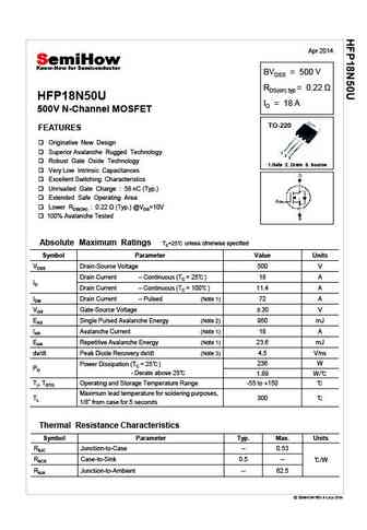
Apr 2014 BVDSS = 500 V RDS(on) typ = 0.22 HFP18N50U ID = 18 A 500V N-Channel MOSFET TO-220 FEATURES Originative New Design Superior Avalanche Rugged Technology 1 2 3 Robust Gate Oxide Technology 1.Gate 2. Drain 3. Source Very Low Intrinsic Capacitances Excellent Switching Characteristics Unrivalled Gate Charge 58 nC (Typ.) Extended Safe Operating Area Low
hfh18n50s.pdf
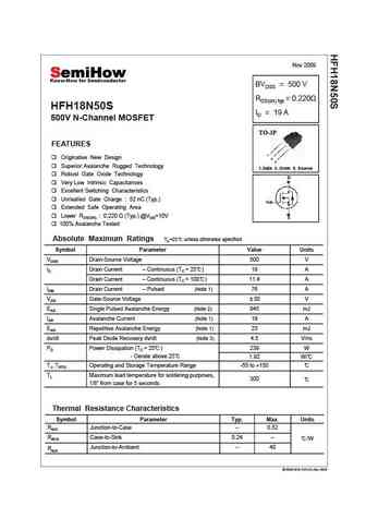
Nov 2009 BVDSS = 500 V RDS(on) typ = 0.220 HFH18N50S ID = 19 A 500V N-Channel MOSFET TO-3P FEATURES 1 Originative New Design 2 3 Superior Avalanche Rugged Technology 1.Gate 2. Drain 3. Source Robust Gate Oxide Technology Very Low Intrinsic Capacitances Excellent Switching Characteristics Unrivalled Gate Charge 52 nC (Typ.) Extended Safe Operating Area Lower RDS(ON
sl18n50f.pdf
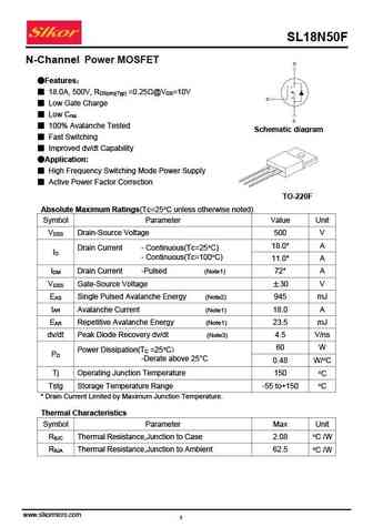
SL18N50F N-Channel Power MOSFET Features 18.0A, 500V, R =0.25 @V =10V DS(on)(Typ) GS Low Gate Charge Low C rss 100% Avalanche Tested Schematic diagram Fast Switching Improved dv/dt Capability Application High Frequency Switching Mode Power Supply Active Power Factor Correction TO-220F Absolute Maximum Ratings(Tc=25 C unless otherwi
tsf18n50mr.pdf

TSF18N50MR 500V N-Channel MOSFET General Description Features This Power MOSFET is produced using Truesemi s 18.0A,500V,Max.RDS(on)=0.32 @ VGS =10V advanced planar stripe DMOS technology. This advanced technology has been especially tailored to Low gate charge(typical 45nC) minimize on-state resistance, provide superior switching High ruggedness performance, and with
tsa18n50mr.pdf
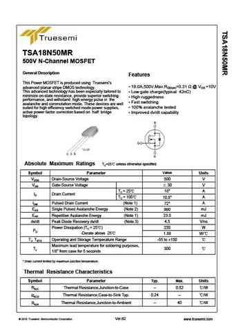
TSA18N50MR 500V N-Channel MOSFET General Description Features This Power MOSFET is produced using Truesemi s 18.0A,500V,Max.RDS(on)=0.31 @ VGS =10V advanced planar stripe DMOS technology. This advanced technology has been especially tailored to Low gate charge(typical 42nC) minimize on-state resistance, provide superior switching High ruggedness performance, and with
wmk18n50d1b wml18n50d1b wmj18n50d1b.pdf
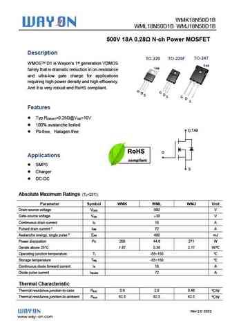
WMK18N50D1B WML18N50D1B WMJ18N50D1B 500V 18A 0.28 N-ch Power MOSFET Description TO-247 TO-220 TO-220F WMOSTM D1 is Wayon s 1st generation VDMOS TAB TAB family that is dramatic reduction in on-resistance and ultra-low gate charge for applications requiring high power density and high efficiency. And it is very robust and RoHS compliant. G D S G D S G D S
wml18n50c4 wmo18n50c4 wmk18n50c4 wmn18n50c4 wmm18n50c4 wmj18n50c4.pdf
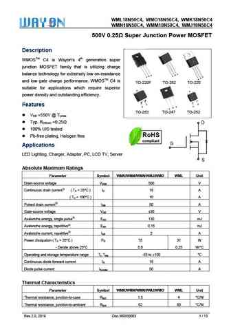
WML18N50C4, WMO18N5 WM C4 W 50C4, MK18N50C WMN18N50C4, WMM18N50C4, WM C4 MJ18N50C 500V 0.25 S T V Super Junction Power MOSFET Descrip ption WMOSTM C4 is Wa 4th generation super ayon s n junction MOSFET fa that is utilizing charge M amily S balance te or extremely esistance echnology fo y low on-re S D D G G G S D G and low ga charge performanc WMOSTM C
cs18n50f cs18n50p cs18n50v cs18n50w.pdf
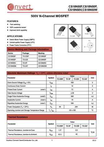
CS18N50F,CS18N50P, nvert Suzhou Convert Semiconductor Co ., Ltd. CS18N50V,CS18N50W 500V N-Channel MOSFET FEATURES Fast switching 100% avalanche tested Improved dv/dt capability APPLICATIONS Switch Mode Power Supply (SMPS) Uninterruptible Power Supply (UPS) Power Factor Correction (PFC) Device Marking and Package Information Device Package Marking CS18N50F
cs18n50f cs18n50p cs18n50v.pdf
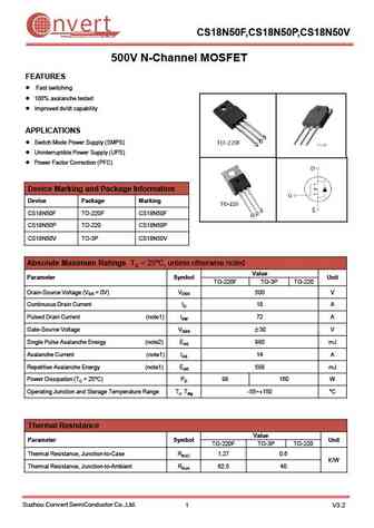
nvert CS18N50F,CS18N50P,CS18N50V Suzhou Convert Semiconductor Co ., Ltd. 500V N-Channel MOSFET FEATURES Fast switching 100% avalanche tested Improved dv/dt capability APPLICATIONS Switch Mode Power Supply (SMPS) Uninterruptible Power Supply (UPS) Power Factor Correction (PFC) Device Marking and Package Information Device Package Marking CS18N50F TO-220F CS1
fir18n50fg.pdf
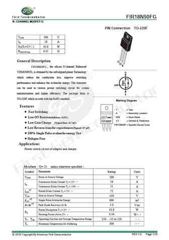
FIR18N50FG N - CHANNEL MOSFET-G PIN Connection TO-220F VDSS 500 V ID 18 A PD(TC=25 ) 42.8 W RDS(ON)Typ 0.31 General Description G D S , the silicon N-channel Enhanced FIR18N50FG VDMOSFETs, is obtained by the self-aligned planar Technology D which reduce the conduction loss, improve switching performance and enhance the avalanche energy. The transistor G can b
jmpc18n50bj.pdf
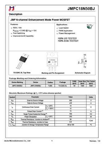
JMPC18N50BJ Description JMP N-channel Enhancement Mode Power MOSFET Features Applications 500V, 18A Load Switch RDS(ON)
jmpf18n50bj.pdf
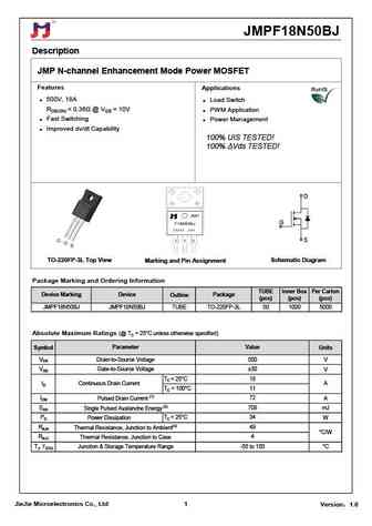
JMPF18N50BJ Description JMP N-channel Enhancement Mode Power MOSFET Features Applications 500V, 18A Load Switch RDS(ON)
lnc18n50 lnd18n50.pdf
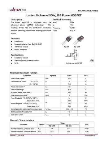
LNC18N50/LND18N50 Lonten N-channel 500V, 18A Power MOSFET Description Product Summary The Power MOSFET is fabricated using the V 500V DSS advanced planar VDMOS technology. The I 18A D resulting device has low conduction resistance, R 0.28 DS(on),max superior switching performance and high avalanche Q 50.5 nC g,typ energy. Features Low R DS(on) Low gate charge (typ. Q =5
spc18n50g.pdf
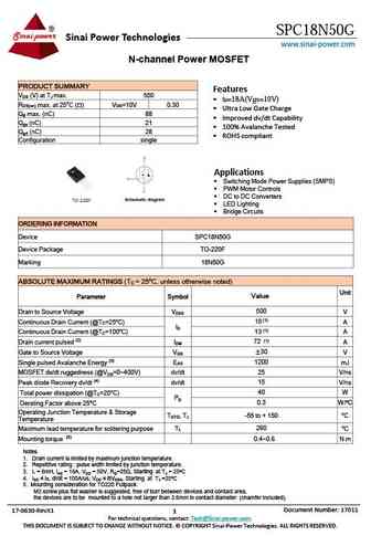
SPC18N50G Sinai Power Technologies www.sinai-power.com N-channel Power MOSFET PRODUCT SUMMARY Features V (V) at T max. 550 DS J ID=18A(Vgs=10V) R max. at 25oC ( ) V =10V 0.30 DS(on) GS Ultra Low Gate Charge Q max. (nC) 88 g Improved dv/dt Capability Q (nC) 21 gs 100% Avalanche Tested Q (nC) 28 gd ROHS compliant Configuration single Ap
smirf18n50.pdf
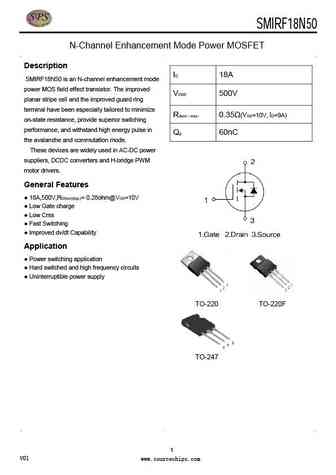
SMIRF18N50 30V /36A Single N Power MOSFET N-Channel Enhancement Mode Power MOSFET Description ID 18A SMIRF18N50 is an N-channel enhancement mode power MOS field effect transistor. The improved VDSS 500V planar stripe cell and the improved guard ring terminal have been especially tailored to minimize Rdson max 0.35 (VGS=10V, ID=9A) on-state resistance, provide superior
vbzmb18n50.pdf
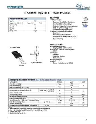
VBZMB18N50 www.VBsemi.com N-Channel (D-S) Power MOSFET 550V FEATURES PRODUCT SUMMARY Optimal Design VDS (V) 550 - Low Area Specific On-Resistance RDS(on) max. at 25 C ( ) VGS = 10 V 0.26 - Low Input Capacitance (Ciss) Qg max. (nC) 150 - Reduced Capacitive Switching Losses Qgs (nC) 12 - High Body Diode Ruggedness Qgd (nC) 25 - Avalanche Energy Rated (UIS) Configuration
hm18n50a hm18n50f.pdf
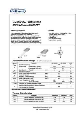
HM18N50A / HM18N50F 500V N-Channel MOSFET General Description Features This Power MOSFET is produced using Maple semi s - 18A, 500V, RDS(on)typ. = 236m @VGS = 10 V advanced planar stripe DMOS technology. - Low gate charge ( typical 69nC) This advanced technology has been especially tailored - High ruggedness to minimize on-state resistance, provide superior switching - Fast switching
fxn18n50f.pdf
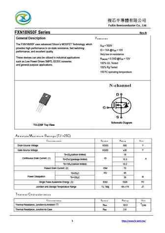
FuXin Semiconductor Co., Ltd. FXN18N50F Series Rev.A General Description Features The FXN18N50F uses advanced Silicon s MOSFET Technology, which V = 500V DS provides high performance in on-state resistance, fast switching ID = 18A @V = 10V GS performance, and excellent quality. Very low on-resistance These devices can also be utilized in ind
mdf18n50th.pdf
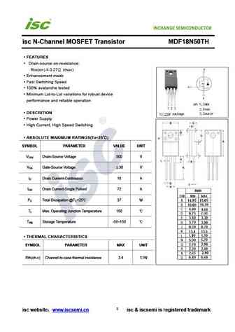
isc N-Channel MOSFET Transistor MDF18N50TH FEATURES Drain-source on-resistance RDS(on) 0.27 (max) Enhancement mode Fast Switching Speed 100% avalanche tested Minimum Lot-to-Lot variations for robust device performance and reliable operation DESCRITION Power Supply High Current, High Speed Switching ABSOLUTE MAXIMUM RATINGS(T =25 ) a SYMBOL PARAMETER
mdp18n50bth.pdf
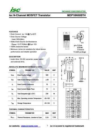
isc N-Channel MOSFET Transistor MDP18N50BTH FEATURES Drain Current I = 18A@ T =25 D C Drain Source Voltage V = 500V(Min) DSS Static Drain-Source On-Resistance R = 0.27 (Max) @V = 10V DS(on) GS 100% avalanche tested Minimum Lot-to-Lot variations for robust device performance and reliable operation DESCRIPTION motor drive, DC-DC converter, power switch and sol
mdq18n50gtp.pdf
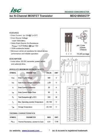
isc N-Channel MOSFET Transistor MDQ18N50GTP FEATURES Drain Current I = 20A@ T =25 D C Drain Source Voltage V = 500V(Min) DSS Static Drain-Source On-Resistance R = 0.27 (Max) @V = 10V DS(on) GS 100% avalanche tested Minimum Lot-to-Lot variations for robust device performance and reliable operation DESCRIPTION motor drive, DC-DC converter, power switch and sol
mdf18n50bth.pdf

isc N-Channel MOSFET Transistor MDF18N50BTH FEATURES Drain-source on-resistance RDS(on) 0.27 (max) Enhancement mode Fast Switching Speed 100% avalanche tested Minimum Lot-to-Lot variations for robust device performance and reliable operation DESCRITION Power Supply High Current, High Speed Switching ABSOLUTE MAXIMUM RATINGS(T =25 ) a SYMBOL PARAMETER
mdp18n50th.pdf
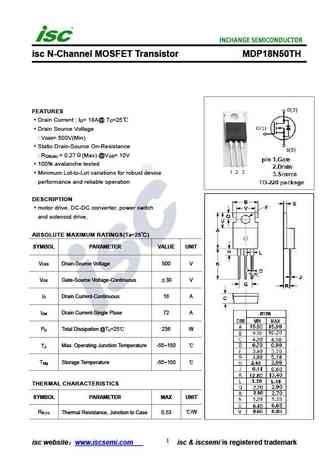
isc N-Channel MOSFET Transistor MDP18N50TH FEATURES Drain Current I = 18A@ T =25 D C Drain Source Voltage V = 500V(Min) DSS Static Drain-Source On-Resistance R = 0.27 (Max) @V = 10V DS(on) GS 100% avalanche tested Minimum Lot-to-Lot variations for robust device performance and reliable operation DESCRIPTION motor drive, DC-DC converter, power switch and sole
18n50mf.pdf
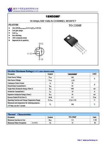
18N50MF 18 Amps,500 Volts N-CHANNEL MOSFET FEATURE TO-220MF 18A,500V,R =0.35 @V =10V/9A DS(ON)MAX GS Low gate charge Low C iss Fast switching 100% avalanche tested Improved dv/dt capability Absolute Maximum Ratings(T =25 ,unless otherwise noted) C Parameter Symbol UNIT 18N50MF Drain-Source Voltage V 500 DSS V Gate-Source Voltage V 30 GSS Continu
Otros transistores... 9N50, 10N50, 11N50, 12N50, 13N50, 14N50, 15N50, 16N50, IRF9540, 24N50, 26N50, UF830, UF830Z, UF840, UK3568, UF450, UF460
Parámetros del MOSFET. Cómo se afectan entre sí.
🌐 : EN ES РУ

Liste
Recientemente añadidas las descripciónes de los transistores:
MOSFET: MSQ60P04D | MSQ40P07D | MSQ30P40D | MSQ30P15 | MSQ30P07D | MSQ100N03D | MSHM60P14 | MSHM40N085 | MSHM30N46 | MSH60N35D | MSH40N032 | MSH30P100 | MSH100N045SA | MSD60P16 | MSD40P45 | MSB100N023
Popular searches
d882p | 2sb1560 | 2n1304 | 2sa979 | 2sc4793 | d965 | mje15031 | irfp150n