1N40 Datasheet. Equivalente. Reemplazo. Hoja de especificaciones. Principales características
Número de Parte: 1N40 📄📄
Tipo de FET: MOSFET
Polaridad de transistor: N
ESPECIFICACIONES MÁXIMAS
Pdⓘ - Máxima disipación de potencia: 25 W
|Vds|ⓘ - Voltaje máximo drenador-fuente: 400 V
|Vgs|ⓘ - Voltaje máximo fuente-puerta: 30 V
|Id|ⓘ - Corriente continua de drenaje: 1.4 A
Tjⓘ - Temperatura máxima de unión: 150 °C
CARACTERÍSTICAS ELÉCTRICAS
trⓘ - Tiempo de subida: 30 nS
Cossⓘ - Capacitancia de salida: 20 pF
RDSonⓘ - Resistencia estado encendido drenaje a fuente: 4.5 Ohm
Encapsulados: TO-220
SOT-92
📄📄 Copiar
Búsqueda de reemplazo de 1N40 MOSFET
- Selecciónⓘ de transistores por parámetros
1N40 datasheet
..1. Size:167K utc
1n40.pdf 
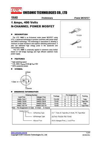
UNISONIC TECHNOLOGIES CO., LTD 1N40 Preliminary Power MOSFET 1 Amps, 400 Volts N-CHANNEL POWER MOSFET DESCRIPTION The UTC 1N40 is an N-channel mode power MOSFET using UTC s advanced technology to provide customers with planar stripe and DMOS technology. This technology is specialized in allowing a minimum on-state resistance and superior switching performance. It also can w
0.1. Size:24K philips
phx1n40e 1.pdf
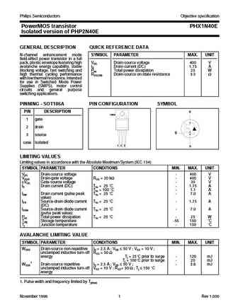
Philips Semiconductors Objective specification PowerMOS transistor PHX1N40E Isolated version of PHP2N40E GENERAL DESCRIPTION QUICK REFERENCE DATA N-channel enhancement mode SYMBOL PARAMETER MAX. UNIT field-effect power transistor in a full pack, plastic envelope featuring high VDS Drain-source voltage 400 V avalanche energy capability, stable ID Drain current (DC) 1.75 A blocking vol
0.2. Size:59K philips
phx1n40 1.pdf
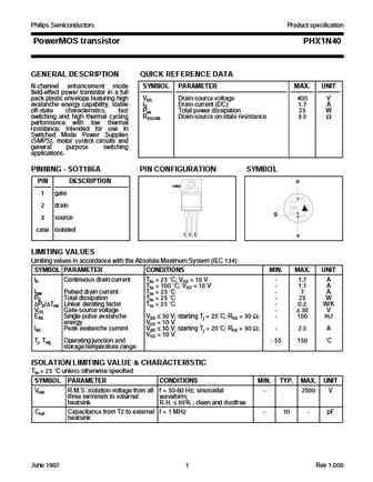
Philips Semiconductors Product specification PowerMOS transistor PHX1N40 GENERAL DESCRIPTION QUICK REFERENCE DATA N-channel enhancement mode SYMBOL PARAMETER MAX. UNIT field-effect power transistor in a full pack plastic envelope featuring high VDS Drain-source voltage 400 V avalanche energy capability, stable ID Drain current (DC) 1.7 A off-state characteristics, fast Ptot Total power
0.3. Size:1213K fairchild semi
fqpf11n40ct.pdf
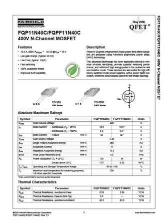
May 2008 QFET FQP11N40C/FQPF11N40C 400V N-Channel MOSFET Features Description 10.5 A, 400V, RDS(on) = 0.5 @VGS = 10 V These N-Channel enhancement mode power field effect transis- tors are produced using Fairchild s proprietary, planar stripe, Low gate charge ( typical 28 nC) DMOS technology. Low Crss ( typical 85pF) This advanced technology has been especially
0.4. Size:970K fairchild semi
fqb11n40ctm.pdf
October 2008 QFET FQB11N40C/FQI11N40C 400V N-Channel MOSFET General Description Features These N-Channel enhancement mode power field effect 10.5 A, 400V, RDS(on) = 0.5 @VGS = 10 V transistors are produced using Fairchild s proprietary, Low gate charge ( typical 28 nC) planar stripe, DMOS technology. Low Crss ( typical 85pF) This advanced technology has been especia
0.5. Size:695K fairchild semi
fqaf11n40.pdf
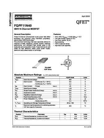
April 2000 TM QFET QFET QFET QFET 400V N-ChanneI MOSFET GeneraI Description Features These N-Channel enhancement mode power field effect 8.8A, 400V, RDS(on) = 0.48 @VGS = 10 V transistors are produced using Fairchild s proprietary, Low gate charge ( typical 27 nC) planar stripe, DMOS technology. Low Crss ( typical 20 pF) This advanced technology has bee
0.6. Size:1216K fairchild semi
fqp11n40c fqpf11n40c.pdf

May 2008 QFET FQP11N40C/FQPF11N40C 400V N-Channel MOSFET Features Description 10.5 A, 400V, RDS(on) = 0.5 @VGS = 10 V These N-Channel enhancement mode power field effect transis- tors are produced using Fairchild s proprietary, planar stripe, Low gate charge ( typical 28 nC) DMOS technology. Low Crss ( typical 85pF) This advanced technology has been especially
0.7. Size:972K fairchild semi
fqb11n40c.pdf
November 2013 FQB11N40C N-Channel QFET MOSFET 400 V, 10.5 A, 530 m Description Features These N-Channel enhancement mode power field effect 10.5 A, 400V, RDS(on) = 530 m (Max.) @ VGS = 10 V, transistors are produced using Fairchild s proprietary, ID = 5.25 A planar stripe, DMOS technology. This advanced Low Gate Charge (Typ. 28 nC) technology has been especially tai
0.8. Size:699K fairchild semi
fqp11n40.pdf
April 2000 TM QFET QFET QFET QFET 400V N-ChanneI MOSFET GeneraI Description Features These N-Channel enhancement mode power field effect 11.4A, 400V, RDS(on) = 0.48 @VGS = 10 V transistors are produced using Fairchild s proprietary, Low gate charge ( typical 27 nC) planar stripe, DMOS technology. Low Crss ( typical 20 pF) This advanced technology has bee
0.9. Size:709K fairchild semi
fqpf11n40t.pdf
April 2000 TM QFET QFET QFET QFET 400V N-ChanneI MOSFET GeneraI Description Features These N-Channel enhancement mode power field effect 6.6A, 400V, RDS(on) = 0.48 @VGS = 10 V transistors are produced using Fairchild s proprietary, Low gate charge ( typical 27 nC) planar stripe, DMOS technology. Low Crss ( typical 20 pF) This advanced technology has been
0.10. Size:565K fairchild semi
fqb11n40tm fqi11n40tu.pdf
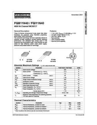
November 2001 FQB11N40 / FQI11N40 400V N-Channel MOSFET General Description Features These N-Channel enhancement mode power field effect 11.4A, 400V, RDS(on) = 0.48 @VGS = 10 V transistors are produced using Fairchild s proprietary, Low gate charge ( typical 27 nC) planar stripe, DMOS technology. Low Crss ( typical 20 pF) This advanced technology has been especially tai
0.11. Size:1039K onsemi
fqb11n40c.pdf

Is Now Part of To learn more about ON Semiconductor, please visit our website at www.onsemi.com Please note As part of the Fairchild Semiconductor integration, some of the Fairchild orderable part numbers will need to change in order to meet ON Semiconductor s system requirements. Since the ON Semiconductor product management systems do not have the ability to manage part nomenclatur
0.12. Size:239K utc
11n40.pdf
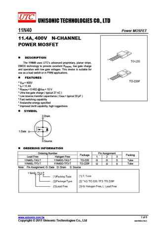
UNISONIC TECHNOLOGIES CO., LTD 11N40 Power MOSFET 11.4A, 400V N-CHANNEL POWER MOSFET DESCRIPTION The 11N40 uses UTC s advanced proprietary, planar stripe, DMOS technology to provide excellent RDS(ON), low gate charge and operation with low gate voltages. This device is suitable for use as a load switch or in PWM applications. FEATURES * VDS = 400V * ID = 11.4A * RD
0.13. Size:1322K kec
khb011n40f1 khb011n40f2 khb011n40p1.pdf

KHB011N40P1/F1/F2 SEMICONDUCTOR N CHANNEL MOS FIELD TECHNICAL DATA EFFECT TRANSISTOR General Description KHB011N40P1 This planar stripe MOSFET has better characteristics, such as fast switching time, low on resistance, low gate charge and excellent avalanche characteristics. It is mainly suitable for electronic ballast and switching mode power supplies. FEATURES VDSS(Min.)= 400V
0.14. Size:56K ape
ap01n40g-hf.pdf
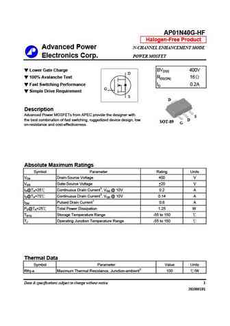
AP01N40G-HF Halogen-Free Product Advanced Power N-CHANNEL ENHANCEMENT MODE Electronics Corp. POWER MOSFET Lower Gate Charge BVDSS 400V D 100% Avalanche Test RDS(ON) 16 Fast Switching Performance ID 0.2A G Simple Drive Requirement S D Description Advanced Power MOSFETs from APEC provide the designer with S the best combination of fast switching, ruggedized device
0.15. Size:57K ape
ap01n40hj-hf.pdf
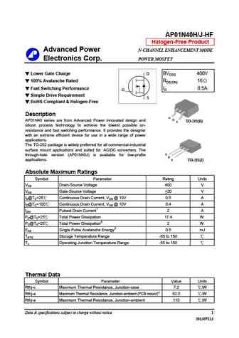
AP01N40H/J-HF Halogen-Free Product Advanced Power N-CHANNEL ENHANCEMENT MODE Electronics Corp. POWER MOSFET Lower Gate Charge BVDSS 400V D 100% Avalanche Rated RDS(ON) 16 Fast Switching Performance ID 0.5A G Simple Drive Requirement S RoHS Compliant & Halogen-Free Description G D AP01N40 series are from Advanced Power innovated design and TO-252(H) S sili
0.16. Size:65K ape
ap01n40j.pdf
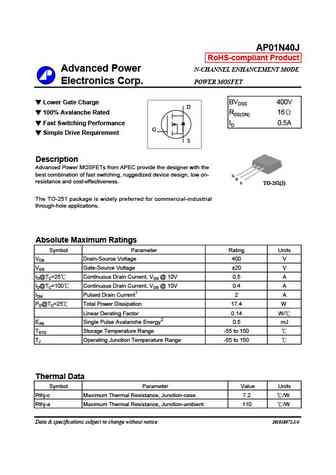
AP01N40J RoHS-compliant Product Advanced Power N-CHANNEL ENHANCEMENT MODE Electronics Corp. POWER MOSFET Lower Gate Charge BVDSS 400V D 100% Avalanche Rated RDS(ON) 16 Fast Switching Performance ID 0.5A G Simple Drive Requirement S Description Advanced Power MOSFETs from APEC provide the designer with the best combination of fast switching, ruggedized device desig
0.17. Size:832K pipsemi
ptp11n40 pta11n40.pdf
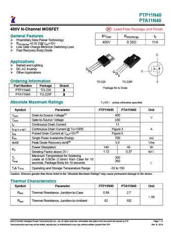
PTP11N40 PTA11N40 400V N-Channel MOSFET General Features BVDSS RDS(ON),typ. ID Proprietary New Planar Technology 400V 0.35 11A RDS(ON),typ.=0.35 @VGS=10V Low Gate Charge Minimize Switching Loss Fast Recovery Body Diode Applications Ballast and Lighting DC-AC Inverter G D S G D Other Applications S Ordering Information TO-220 TO-220F Part Number P
0.18. Size:179K semihow
hfp11n40.pdf
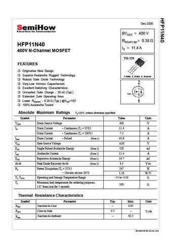
Dec 2005 BVDSS = 400 V RDS(on) typ HFP11N40 ID = 11.4 A 400V N-Channel MOSFET TO-220 FEATURES Originative New Design 1 2 3 Superior Avalanche Rugged Technology 1.Gate 2. Drain 3. Source Robust Gate Oxide Technology Very Low Intrinsic Capacitances Excellent Switching Characteristics Unrivalled Gate Charge 35 nC (Typ.) Extended Safe Operating Area Lower RDS(
0.19. Size:167K semihow
hfs11n40.pdf
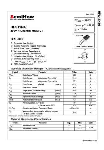
Dec 2005 BVDSS = 400 V RDS(on) typ HFS11N40 ID = 11.4 A 400V N-Channel MOSFET TO-220F FEATURES 1 Originative New Design 2 3 Superior Avalanche Rugged Technology 1.Gate 2. Drain 3. Source Robust Gate Oxide Technology Very Low Intrinsic Capacitances Excellent Switching Characteristics Unrivalled Gate Charge 35 nC (Typ.) Extended Safe Operating Area Lower RD
0.20. Size:169K semihow
hfw11n40.pdf
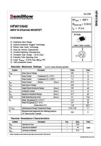
Dec 2005 BVDSS = 400 V RDS(on) typ HFW11N40 ID = 11.4 A 400V N-Channel MOSFET D2-PAK FEATURES Originative New Design Superior Avalanche Rugged Technology 1.Gate 2. Drain 3. Source Robust Gate Oxide Technology Very Low Intrinsic Capacitances Excellent Switching Characteristics Unrivalled Gate Charge 35 nC (Typ.) Extended Safe Operating Area Lower RDS(ON)
0.21. Size:1055K way-on
wmc1n40d1.pdf
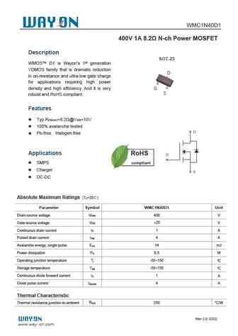
WMC1N40D1 400V 1A 8.2 N-ch Power MOSFET Description SOT-23 WMOSTM D1 is Wayon s 1st generation VDMOS family that is dramatic reduction D in on-resistance and ultra-low gate charge for applications requiring high power density and high efficiency. And it is very G S robust and RoHS compliant. Features Typ.R =8.2 @V =10V DS(on) GS 100% avalanche tested Pb-free H
0.22. Size:2550K first semi
fir11n40fg.pdf
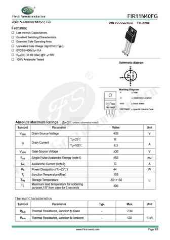
FIR11N40FG 400V N-Channel MOSFET-G PIN Connection TO-220F Features Low Intrinsic Capacitances. Excellent Switching Characteristics. Extended Safe Operating Area. Unrivalled Gate Charge Qg=27nC (Typ.). BVDSS=400V,ID=11A G DS RDS(on) 0.4 (Max) @V =10V G 100% Avalanche Tested g Schematic dia ram D G S Marking Diagram Y = Year A = Assembly Loc
Otros transistores... 3N50, 3N50Z, 4N50, 5N50, 5N50K, 6N50, 7N50, 8N50, AON6380, 2N40, 3N40, 4N40, 5N40, 6N40, 7N40, 8N40, 9N40
