6N40 MOSFET Equivalente. Reemplazo. Hoja de especificaciones. Principales características
Número de Parte: 6N40
Tipo de FET: MOSFET
Polaridad de transistor: N
ESPECIFICACIONES MÁXIMAS
Pdⓘ - Máxima
disipación de potencia: 73 W
|Vds|ⓘ - Voltaje máximo drenador-fuente: 400 V
|Vgs|ⓘ - Voltaje máximo fuente-puerta: 30 V
|Id|ⓘ - Corriente continua
de drenaje: 6 A
Tjⓘ - Temperatura máxima de unión: 150 °C
CARACTERÍSTICAS ELÉCTRICAS
trⓘ - Tiempo
de subida: 65 nS
Cossⓘ - Capacitancia de salida: 80 pF
RDSonⓘ - Resistencia estado encendido drenaje a fuente: 0.8 Ohm
Encapsulados: TO-220
TO-252
TO-220F
Búsqueda de reemplazo de 6N40 MOSFET
- Selecciónⓘ de transistores por parámetros
6N40 datasheet
..1. Size:184K utc
6n40.pdf 

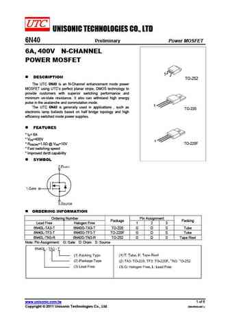
UNISONIC TECHNOLOGIES CO., LTD 6N40 Preliminary Power MOSFET 6A, 400V N-CHANNEL POWER MOSFET 1 DESCRIPTION TO-252 The UTC 6N40 is an N-Channel enhancement mode power MOSFET using UTC s perfect planar stripe, DMOS technology to provide customers with superior switching performance and minimum on-state resistance. It also can withstand high energy pulse in the avalanche and
0.1. Size:40K 1
hgtp6n40e1d hgtp6n50e1d.pdf 

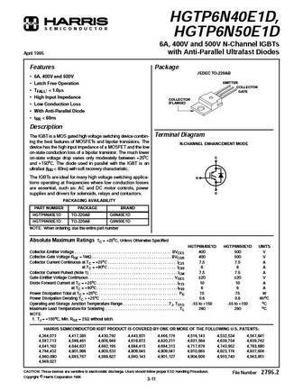
HGTP6N40E1D, S E M I C O N D U C T O R HGTP6N50E1D 6A, 400V and 500V N-Channel IGBTs with Anti-Parallel Ultrafast Diodes April 1995 Features Package JEDEC TO-220AB 6A, 400V and 500V EMITTER Latch Free Operation COLLECTOR TFALL
0.2. Size:32K 1
hgtd6n40e1 hgtd6n40e1s hgtd6n50e1 hgtd6n50e1s.pdf 

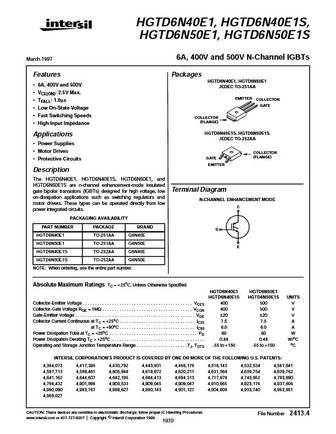
HGTD6N40E1, HGTD6N40E1S, HGTD6N50E1, HGTD6N50E1S 6A, 400V and 500V N-Channel IGBTs March 1997 Features Packages HGTD6N40E1, HGTD6N50E1 6A, 400V and 500V JEDEC TO-251AA VCE(ON) 2.5V Max. EMITTER COLLECTOR TFALL 1.0 s GATE Low On-State Voltage Fast Switching Speeds COLLECTOR (FLANGE) High Input Impedance HGTD6N40E1S, HGTD6N50E1S Applications JEDEC TO
0.3. Size:217K motorola
mtw16n40erev3.pdf 

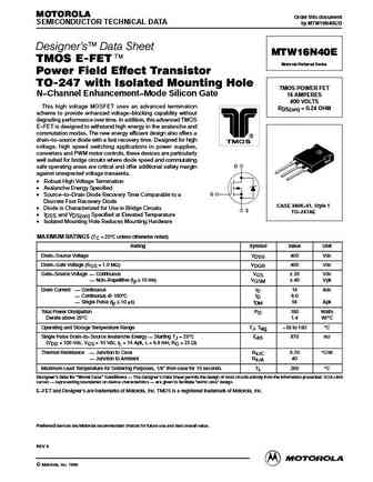
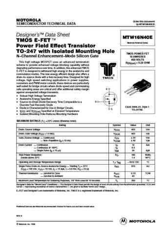
MOTOROLA Order this document SEMICONDUCTOR TECHNICAL DATA by MTW16N40E/D Designer's Data Sheet MTW16N40E TMOS E-FET. Motorola Preferred Device Power Field Effect Transistor TO-247 with Isolated Mounting Hole TMOS POWER FET N Channel Enhancement Mode Silicon Gate 16 AMPERES 400 VOLTS This high voltage MOSFET uses an advanced termination RDS(on) = 0.24 OHM scheme to provi
0.4. Size:145K motorola
mtw16n40e.pdf 

MOTOROLA Order this document SEMICONDUCTOR TECHNICAL DATA by MTW16N40E/D Designer's Data Sheet MTW16N40E TMOS E-FET. Motorola Preferred Device Power Field Effect Transistor TO-247 with Isolated Mounting Hole TMOS POWER FET N Channel Enhancement Mode Silicon Gate 16 AMPERES 400 VOLTS This high voltage MOSFET uses an advanced termination RDS(on) = 0.24 OHM scheme to provi
0.6. Size:206K toshiba
ssm6n40tu.pdf 

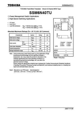
SSM6N40TU TOSHIBA Field-Effect Transistor Silicon N Channel MOS Type SSM6N40TU Power Management Switch Applications Unit mm 2.1 0.1 High-Speed Switching Applications 1.7 0.1 4 V drive N-ch 2-in-1 1 6 Low ON-resistance Ron = 182m (max) (@VGS = 4 V) 2 5 Ron = 122m (max) (@VGS = 10 V) 3 4 Absolute Maximum Ratings (Ta = 25 C) (Q1, Q2 Common)
0.7. Size:654K fairchild semi
fqd6n40ctf fqd6n40ctm fqd6n40c fqu6n40c fqu6n40ctu.pdf 

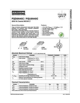
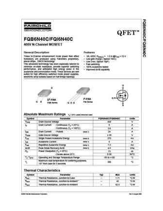
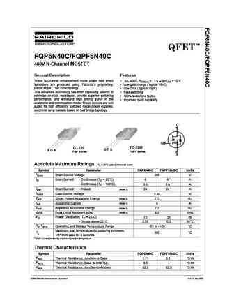
October 2008 QFET FQD6N40C / FQU6N40C 400V N-Channel MOSFET General Description Features These N-Channel enhancement mode power field effect 4.5A, 400V, RDS(on) = 1.0 @VGS = 10 V transistors are produced using Fairchild s proprietary, Low gate charge ( typical 16nC) planar stripe, DMOS technology. Low Crss ( typical 15pF) This advanced technology has been especiall
0.10. Size:756K fairchild semi
fqb6n40c.pdf 

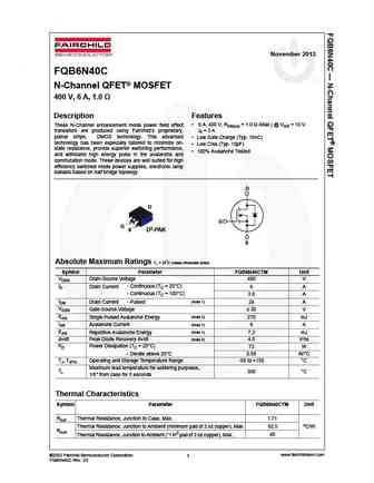
November 2013 FQB6N40C N-Channel QFET MOSFET 400 V, 6 A, 1.0 Description Features These N-Channel enhancement mode power field effect 6 A, 400 V, RDS(on) = 1.0 (Max.) @ VGS = 10 V, transistors are produced using Fairchild s proprietary, ID = 3 A planar stripe, DMOS technology. This advanced Low Gate Charge (Typ. 16nC) technology has been especially tailored to min
0.11. Size:1088K fairchild semi
fqp6n40cf fqpf6n40cf.pdf 

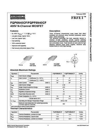
February 2006 TM FRFET FQP6N40CF/FQPF6N40CF 400V N-Channel MOSFET Features Description 6A, 400V, RDS(on) = 1.1 @VGS = 10 V These N-Channel enhancement mode power field effect transistors are produced using Fairchild s proprietary, planar Low gate charge ( typical 16nC) stripe, DMOS technology. This advanced technology has been especially tailored to Low Crss ( typi
0.12. Size:723K fairchild semi
fqd6n40tf fqd6n40tm.pdf 

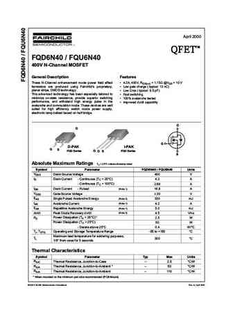
April 2000 TM QFET QFET QFET QFET FQD6N40 / FQU6N40 400V N-ChanneI MOSFET GeneraI Description Features These N-Channel enhancement mode power field effect 4.2A, 400V, RDS(on) = 1.15 @VGS = 10 V transistors are produced using Fairchild s proprietary, Low gate charge ( typical 13 nC) planar stripe, DMOS technology. Low Crss ( typical 9.5 pF) This advanced technolog
0.14. Size:567K fairchild semi
fdp26n40 fdpf26n40.pdf 

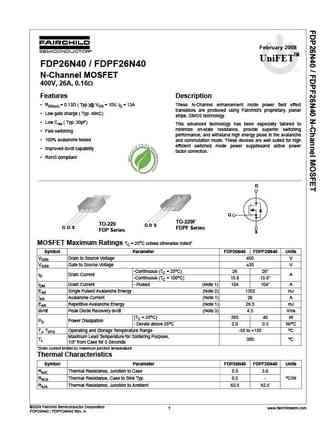
February 2008 UniFETTM FDP26N40 / FDPF26N40 tm N-Channel MOSFET 400V, 26A, 0.16 Features Description RDS(on) = 0.13 ( Typ.)@ VGS = 10V, ID = 13A These N-Channel enhancement mode power field effect transistors are produced using Fairchild s proprietary, planar Low gate charge ( Typ. 48nC) stripe, DMOS technology. Low Crss ( Typ. 30pF) This advanced technology h
0.15. Size:173K vishay
sihf6n40d.pdf 

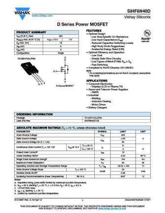
SiHF6N40D www.vishay.com Vishay Siliconix D Series Power MOSFET FEATURES PRODUCT SUMMARY Optimal Design VDS (V) at TJ max. 450 - Low Area Specific On-Resistance RDS(on) max. at 25 C ( ) VGS = 10 V 1.0 - Low Input Capacitance (Ciss) Qg max. (nC) 18 - Reduced Capacitive Switching Losses Qgs (nC) 3 - High Body Diode Ruggedness - Avalanche Energy Rated (UIS) Qgd (nC) 4 O
0.16. Size:214K vishay
sihp6n40d.pdf 

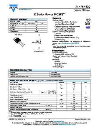
SiHP6N40D www.vishay.com Vishay Siliconix D Series Power MOSFET FEATURES PRODUCT SUMMARY Optimal Design VDS (V) at TJ max. 450 - Low Area Specific On-Resistance RDS(on) max. at 25 C ( ) VGS = 10 V 1.0 - Low Input Capacitance (Ciss) Qg max. (nC) 18 - Reduced Capacitive Switching Losses Qgs (nC) 3 - High Body Diode Ruggedness Qgd (nC) 4 - Avalanche Energy Rated (UIS) Conf
0.17. Size:1303K onsemi
fqp6n40c.pdf 

Is Now Part of To learn more about ON Semiconductor, please visit our website at www.onsemi.com Please note As part of the Fairchild Semiconductor integration, some of the Fairchild orderable part numbers will need to change in order to meet ON Semiconductor s system requirements. Since the ON Semiconductor product management systems do not have the ability to manage part nomenclatur
0.18. Size:892K onsemi
fqb6n40c.pdf 

Is Now Part of To learn more about ON Semiconductor, please visit our website at www.onsemi.com Please note As part of the Fairchild Semiconductor integration, some of the Fairchild orderable part numbers will need to change in order to meet ON Semiconductor s system requirements. Since the ON Semiconductor product management systems do not have the ability to manage part nomenclatur
0.19. Size:940K onsemi
fqd6n40c.pdf 

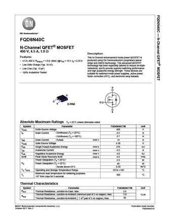
FQD6N40C N-Channel QFET MOSFET 400 V, 4.5 A, 1.0 Description Features This N-Channel enhancement mode power MOSFET is produced using ON Semiconductor s proprietary planar 4.5 A, 400 V, RDS(on) = 1.0 (Max.) @VGS = 10 V, ID = 2.25 A stripe and DMOS technology. This advanced MOSFET Low Gate Charge (Typ. 16 nC) technology has been especially tailored to reduce on-st
0.20. Size:40K harris semi
hgtp6n40.pdf 

HGTP6N40E1D, S E M I C O N D U C T O R HGTP6N50E1D 6A, 400V and 500V N-Channel IGBTs with Anti-Parallel Ultrafast Diodes April 1995 Features Package JEDEC TO-220AB 6A, 400V and 500V EMITTER Latch Free Operation COLLECTOR TFALL
0.21. Size:555K silikron
ssf6n40d.pdf 

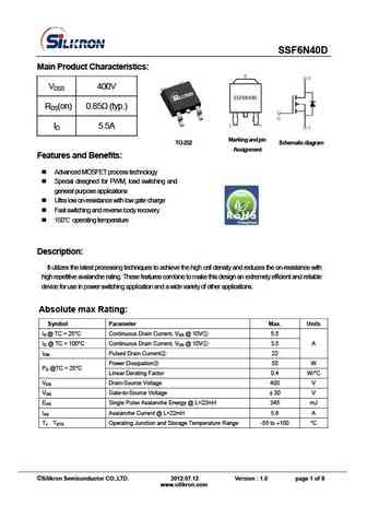
SSF6N40D Main Product Characteristics VDSS 400V RDS(on) 0.85 (typ.) ID 5.5A TO-252 Marking a nd p in Sche ma ti c di agr a m Assignment Features and Benefits Advanced MOSFET process technology Special designed for PWM, load switching and general purpose applications Ultra low on-resistance with low gate charge Fast switching and reverse body recover
0.22. Size:120K jdsemi
cm6n40c.pdf 

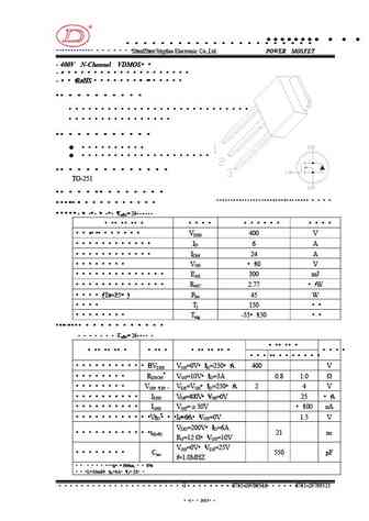
R C64C MN0 www.jdsemi.cn ShenZhen Jingdao Electronic Co.,Ltd. POWER MOSFET 400V N-Channel VDMOS RoHS 1 2 3 TO-2
0.23. Size:123K jdsemi
cm6n40.pdf 

R C64 MN0 www.jdsemi.cn ShenZhen Jingdao Electronic Co.,Ltd. POWER MOSFET 400V N-Channel VDMOS RoHS 1 2 3 TO-22
0.24. Size:1601K bruckewell
msq6n40.pdf 

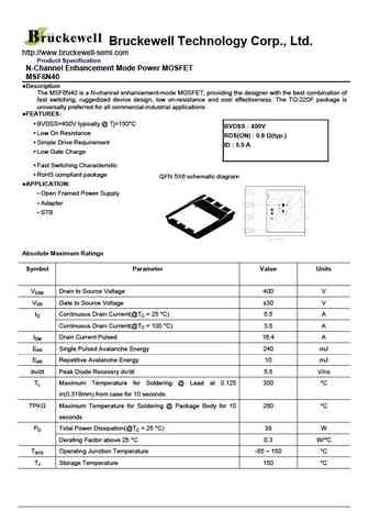
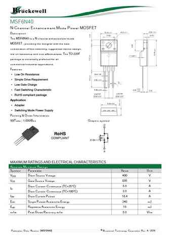
Bruckewell Technology Corp., Ltd. http //www.bruckewell-semi.com Product Specification N-Channel Enhancement Mode Power MOSFET MSF6N40 Description The MSF6N40 is a N-channel enhancement-mode MOSFET, providing the designer with the best combination of fast switching, ruggedized device design, low on-resistance and cost effectiveness. The TO-220F package is universally prefer
0.25. Size:847K bruckewell
ms6n40.pdf 

MS6N40 N-Channel Enhancement Mode Power MOSFET Description The MS6N40 is a N-channel enhancement-mode MOSFET, providing the designer with the best combination of fast switching, ruggedized device design, low on-resistance and cost effectiveness. The TO-220 package is universally preferred for all commercial-industrial applications Features BVDSS=650V typically @ Tj=150
0.26. Size:881K bruckewell
msf6n40.pdf 

MSF6N40 N-Channel Enhancement Mode Power MOSFET Description The MSF6N40 is a N-channel enhancement-mode MOSFET , providing the designer with the best combination of fast switching, ruggedized device design, low on-resistance and cost effectiveness. The TO-220F package is universally preferred for all commercial-industrial applications Features Low On Resistance Sim
0.27. Size:1139K belling
bl6n40-p bl6n40-a bl6n40-u bl6n40-d.pdf 

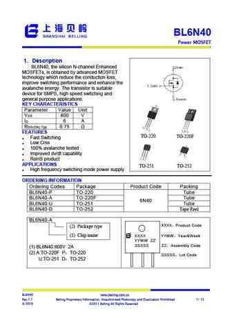
BL6N40 Power MOSFET 1 Description Step-Down Converter BL6N40, the silicon N-channel Enhanced , MOSFETs, is obtained by advanced MOSFET technology which reduce the conduction loss, improve switching performance and enhance the avalanche energy. The transistor is suitable device for SMPS, high speed switching and general purpose applications. KEY CHARACTERISTICS Para
0.28. Size:894K pipsemi
psa06n40 psp06n40.pdf 

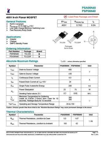
PSA06N40 PSP06N40 400V N-ch Planar MOSFET General Features BVDSS RDS(ON),Typ. ID RoHS Compliant 400V 0.78 6.0A RDS(ON),typ.=0.78 @VGS=10V Low Gate Charge Minimize Switching Loss Fast Recovery Body Diode Applications Adaptor Charger SMPS Standby Power Ordering Information Part Number Package Brand PSP06N40 TO-220 PSA06N40 TO-220F Absolute Maximum Ra
0.29. Size:256K semiwell
sfp6n40.pdf 

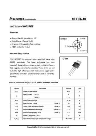
SemiWell Semiconductor SFP6N40 N-Channel MOSFET Features RDS(ON) Max 1.0 ohm at VGS = 10V Gate Charge ( Typical 18nC) Improve dv/dt capability, Fast switching 100% avalanche Tested General Description This MOSFET is produced using advanced planar strip DMOS technology. This latest technology has been especially designed to minimize on-state resistance have
0.30. Size:23K shaanxi
mtm26n40e.pdf 

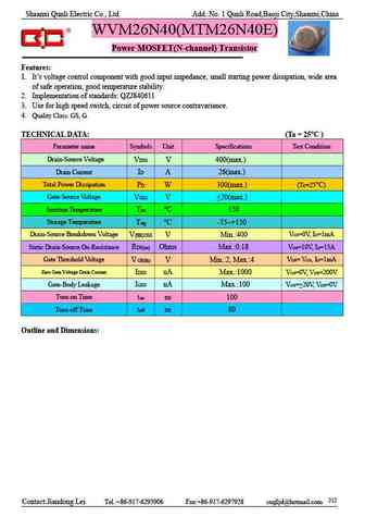
Shaanxi Qunli Electric Co., Ltd Add. No. 1 Qunli Road,Baoji City,Shaanxi,China WVM26N40(MTM26N40E) Power MOSFET(N-channel) Transistor Features 1. It s voltage control component with good input impedance, small starting power dissipation, wide area of safe operation, good temperature stability. 2. Implementation of standards QZJ840611 3. Use for high speed switch, circuit of pow
0.31. Size:2904K first semi
fir6n40fg.pdf 

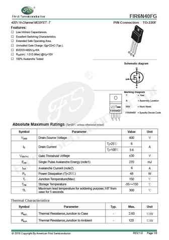
FIR6N40FG 400V N-Channel MOSFET -T PIN Connection TO-220F Features Low Intrinsic Capacitances. Excellent Switching Characteristics. Extended Safe Operating Area. Unrivalled Gate Charge Qg=22nC (Typ.). BVDSS=400V,ID=6A G RDS(on) 1.0 (Max) @VG=10V D S 100% Avalanche Tested g Schematic dia ram D G S Marking Diagram Y = Year A = Assembly
0.32. Size:259K inchange semiconductor
fdp26n40.pdf 
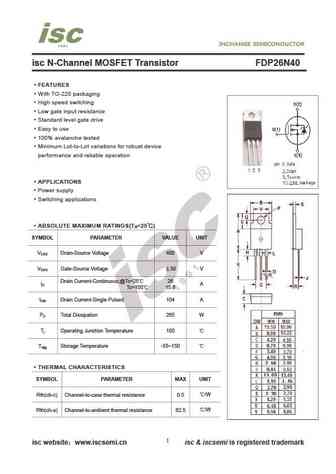
isc N-Channel MOSFET Transistor FDP26N40 FEATURES With TO-220 packaging High speed switching Low gate input resistance Standard level gate drive Easy to use 100% avalanche tested Minimum Lot-to-Lot variations for robust device performance and reliable operation APPLICATIONS Power supply Switching applications ABSOLUTE MAXIMUM RATINGS(T =25 ) a SYMBOL PAR
0.33. Size:1458K cn apm
ap6n40d.pdf 

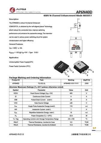
AP6N40D 400V N-Channel Enhancement Mode MOSFET Description The AP6N40D is silicon N-channel Enhanced VDMOSFETs, is obtained by the self-aligned planar Technology which reduce the conduction loss, improve switching performance and enhance the avalanche energy. The transistor can be used in various power switching circuit for system miniaturization and higher efficiency. Genera
Otros transistores... 6N50
, 7N50
, 8N50
, 1N40
, 2N40
, 3N40
, 4N40
, 5N40
, AON6380
, 7N40
, 8N40
, 9N40
, 10N40
, 11N40
, 12N40
, 13N40
, 15N40
.
History: MEE7636-G
