20N40 MOSFET Equivalente. Reemplazo. Hoja de especificaciones. Principales características
Número de Parte: 20N40
Tipo de FET: MOSFET
Polaridad de transistor: N
ESPECIFICACIONES MÁXIMAS
Pdⓘ - Máxima
disipación de potencia: 235 W
|Vds|ⓘ - Voltaje máximo drenador-fuente: 400 V
|Vgs|ⓘ - Voltaje máximo fuente-puerta: 30 V
|Id|ⓘ - Corriente continua
de drenaje: 23 A
Tjⓘ - Temperatura máxima de unión: 150 °C
CARACTERÍSTICAS ELÉCTRICAS
trⓘ - Tiempo
de subida: 92 nS
Cossⓘ - Capacitancia de salida: 370 pF
RDSonⓘ - Resistencia estado encendido drenaje a fuente: 0.15 Ohm
Encapsulados: TO-247
Búsqueda de reemplazo de 20N40 MOSFET
- Selecciónⓘ de transistores por parámetros
20N40 datasheet
..1. Size:195K utc
20n40.pdf 
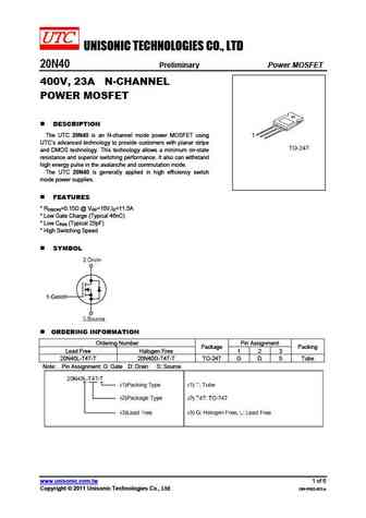
UNISONIC TECHNOLOGIES CO., LTD 20N40 Preliminary Power MOSFET 400V, 23A N-CHANNEL POWER MOSFET DESCRIPTION The UTC 20N40 is an N-channel mode power MOSFET using UTC s advanced technology to provide customers with planar stripe and DMOS technology. This technology allows a minimum on-state resistance and superior switching performance. It also can withstand high energy pulse
0.1. Size:186K 1
sgr20n40l sgu20n40l.pdf
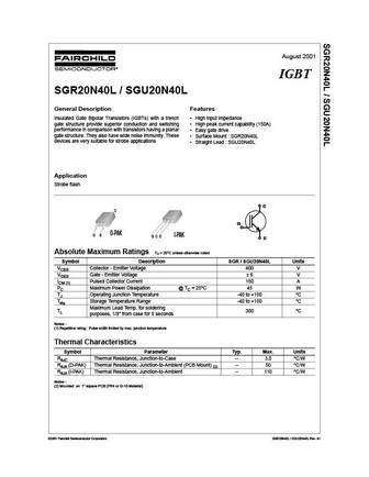
August 2001 IGBT SGR20N40L / SGU20N40L General Description Features Insulated Gate Bipolar Transistors (IGBTs) with a trench High input impedance gate structure provide superior conduction and switching High peak current capability (150A) performance in comparison with transistors having a planar Easy gate drive gate structure. They also have wide noise immunity. These
0.2. Size:133K motorola
mgp20n40clrev1.pdf

MOTOROLA Order this document SEMICONDUCTOR TECHNICAL DATA by MGP20N40CL/D Advanced Information MGP20N40CL SMARTDISCRETES Internally Clamped, N-Channel IGBT 20 AMPERES This Logic Level Insulated Gate Bipolar Transistor (IGBT) VOLTAGE CLAMPED features Gate Emitter ESD protection, Gate Collector overvoltage N CHANNEL IGBT protection from SMARTDISCRETES monolithic circuitr
0.3. Size:157K motorola
mtu20n40erev1.pdf
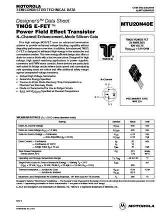
MOTOROLA Order this document SEMICONDUCTOR TECHNICAL DATA by MTU20N40E/D Designer's Data Sheet MTU20N40E TMOS E-FET. Power Field Effect Transistor N Channel Enhancement Mode Silicon Gate TMOS POWER FET This high voltage MOSFET uses an advanced termination 20 AMPERES scheme to provide enhanced voltage blocking capability without 400 VOLTS degrading performance over time
0.4. Size:162K motorola
mtu20n40e.pdf

MOTOROLA Order this document SEMICONDUCTOR TECHNICAL DATA by MTU20N40E/D Designer's Data Sheet MTU20N40E TMOS E-FET. Power Field Effect Transistor N Channel Enhancement Mode Silicon Gate TMOS POWER FET This high voltage MOSFET uses an advanced termination 20 AMPERES scheme to provide enhanced voltage blocking capability without 400 VOLTS degrading performance over time
0.5. Size:138K motorola
mgp20n40cl.pdf
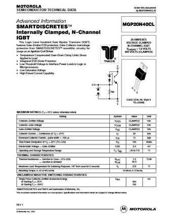
MOTOROLA Order this document SEMICONDUCTOR TECHNICAL DATA by MGP20N40CL/D Advanced Information MGP20N40CL SMARTDISCRETES Internally Clamped, N-Channel IGBT 20 AMPERES This Logic Level Insulated Gate Bipolar Transistor (IGBT) VOLTAGE CLAMPED features Gate Emitter ESD protection, Gate Collector overvoltage N CHANNEL IGBT protection from SMARTDISCRETES monolithic circuitr
0.6. Size:488K fairchild semi
fdbl0120n40.pdf
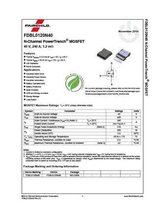
November 2014 FDBL0120N40 N-Channel PowerTrench MOSFET 40 V, 240 A, 1.2 m Features Typical RDS(on) = 0.9 m at VGS = 10V, ID = 80 A Typical Qg(tot) = 90 nC at VGS = 10V, ID = 80 A UIS Capability D RoHS Compliant Applications Industrial Motor Drive G Industrial Power Supply Industrial Automation Battery Operated tools S Battery Protection For current package
0.7. Size:150K fairchild semi
fdh20n40 fdp20n40.pdf
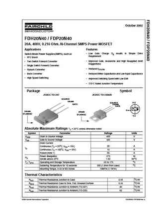
October 2002 FDH20N40 / FDP20N40 20A, 400V, 0.216 Ohm, N-Channel SMPS Power MOSFET Applications Features Low Gate Charge Qg results in Simple Drive Switch Mode Power Supplies(SMPS), such as Requirement PFC Boost Improved Gate, Avalanche and High Reapplied dv/dt Two-Switch Forward Converter Ruggedness Single Switch Forward Converter Reduced rDS(ON) Flyb
0.8. Size:712K fairchild semi
fqa20n40.pdf
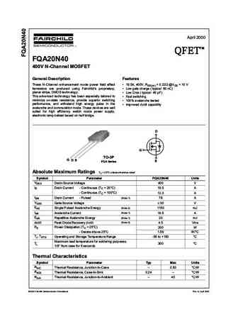
April 2000 TM QFET QFET QFET QFET 400V N-ChanneI MOSFET GeneraI Description Features These N-Channel enhancement mode power field effect 19.5A, 400V, RDS(on) = 0.22 @VGS = 10 V transistors are produced using Fairchild s proprietary, Low gate charge ( typical 60 nC) planar stripe, DMOS technology. Low Crss ( typical 45 pF) This advanced technology has bee
0.9. Size:174K samsung
sgr20n40l.pdf
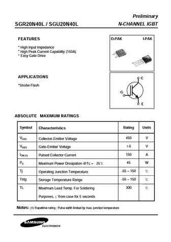
Preliminary N-CHANNEL IGBT SGR20N40L / SGU20N40L D-PAK I-PAK FEATURES * High Input Impedance * High Peak Current Capability (150A) * Easy Gate Drive APPLICATIONS C *Strobe Flash G E ABSOLUTE MAXIMUM RATINGS Symbol Rating Units Characteristics VCES 450 V Collector-Emitter Voltage VGES 6 V Gate-Emitter Voltage ICM (1) 150 A Pulsed Collector Current PC 45 W Maximum Power
0.10. Size:582K onsemi
fdbl0120n40.pdf

Is Now Part of To learn more about ON Semiconductor, please visit our website at www.onsemi.com Please note As part of the Fairchild Semiconductor integration, some of the Fairchild orderable part numbers will need to change in order to meet ON Semiconductor s system requirements. Since the ON Semiconductor product management systems do not have the ability to manage part nomenclatur
0.11. Size:331K aosemi
aotf20n40.pdf
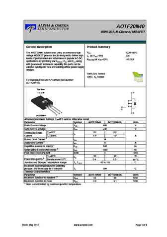
AOTF20N40 400V,20A N-Channel MOSFET General Description Product Summary VDS 500@150 The AOTF20N40 is fabricated using an advanced high voltage MOSFET process that is designed to deliver high ID (at VGS=10V) 20A levels of performance and robustness in popular AC-DC RDS(ON) (at VGS=10V)
0.12. Size:457K aosemi
aotf20n40 aotf20n40l.pdf
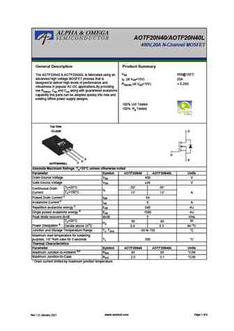
AOTF20N40/AOTF20N40L 400V,20A N-Channel MOSFET General Description Product Summary VDS 500@150 The AOTF20N40 & AOTF20N40L is fabricated using an advanced high voltage MOSFET process that is ID (at VGS=10V) 20A designed to deliver high levels of performance and RDS(ON) (at VGS=10V)
0.13. Size:975K blue-rocket-elect
br20n40.pdf
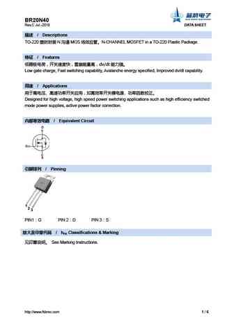
BR20N40 Rev.C Jul.-2018 DATA SHEET / Descriptions TO-220 N MOS N-CHANNEL MOSFET in a TO-220 Plastic Package. / Features dv/dt Low gate charge, Fast switching capability, Avalanche energy specified, Improved dv/dt capability. / Applications
0.14. Size:1210K feihonltd
fhp20n40a.pdf
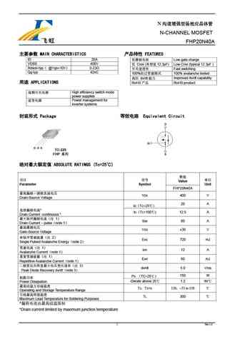
N N-CHANNEL MOSFET FHP20N40A MAIN CHARACTERISTICS FEATURES ID 20A Low gate charge VDSS 400V Crss ( 12.3pF) Low Crss (typical 12.3pF ) Rdson-typ @Vgs=10V 0.23 Fast switching Qg-typ 42nC 100% 100% avalanche tested dv/dt Improved
0.15. Size:573K pipsemi
ptp20n40b pta20n40b.pdf
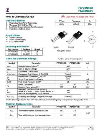
PTP20N40B PTA20N40B 400V N-Channel MOSFET General Features BVDSS RDS(ON),typ. ID Proprietary New Planar Technology 400V 0.24 20A RDS(ON),typ.=0.24 @VGS=10V Low Gate Charge Minimize Switching Loss Fast Recovery Body Diode Applications Adaptor Charger SMPS Power Supply G D S G D LCD Panel Power S Ordering Information TO-220 TO-220F Part Number P
0.16. Size:712K cn minos
mp20n40p.pdf
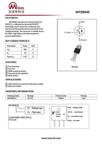
Description MP20N40, the silicon N-channel Enhanced MOSFETs, is obtained by advanced MOSFET technology which reduce the conduction loss, improve switching performance and enhance the avalanche energy. The transistor is suitable device for SMPS, high speed switching and general purpose applications. KEY CHARACTERISTICS Parameter Value Unit V 400 V DS I 20 A D R 0.22 DS(ON).Typ
0.17. Size:251K inchange semiconductor
aotf20n40.pdf
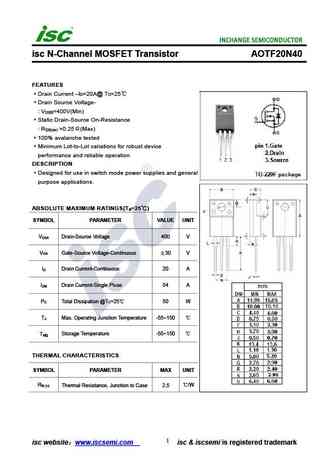
isc N-Channel MOSFET Transistor AOTF20N40 FEATURES Drain Current I =20A@ T =25 D C Drain Source Voltage- V =400V(Min) DSS Static Drain-Source On-Resistance R =0.25 (Max) DS(on) 100% avalanche tested Minimum Lot-to-Lot variations for robust device performance and reliable operation DESCRIPTION Designed for use in switch mode power supplies and general purpos
0.18. Size:300K inchange semiconductor
fdh20n40.pdf
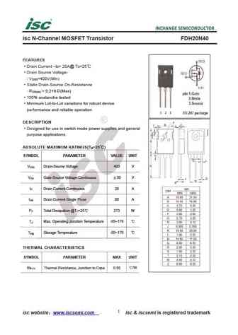
isc N-Channel MOSFET Transistor FDH20N40 FEATURES Drain Current I = 20A@ T =25 D C Drain Source Voltage- V =400V(Min) DSS Static Drain-Source On-Resistance R = 0.216 (Max) DS(on) 100% avalanche tested Minimum Lot-to-Lot variations for robust device performance and reliable operation DESCRIPTION Designed for use in switch mode power supplies and general purp
Otros transistores... 8N40
, 9N40
, 10N40
, 11N40
, 12N40
, 13N40
, 15N40
, 18N40
, 4N60
, 25N40
, UF730
, UF740
, UF3N25
, UF634
, 12N25
, 15N25
, 18N25
.
History: AUIRF2807
