7P20 MOSFET Equivalente. Reemplazo. Hoja de especificaciones. Principales características
Número de Parte: 7P20
Tipo de FET: MOSFET
Polaridad de transistor: P
ESPECIFICACIONES MÁXIMAS
Pdⓘ - Máxima
disipación de potencia: 55 W
|Vds|ⓘ - Voltaje máximo drenador-fuente: 200 V
|Vgs|ⓘ - Voltaje máximo fuente-puerta: 30 V
|Id|ⓘ - Corriente continua
de drenaje: 5.7 A
Tjⓘ - Temperatura máxima de unión: 150 °C
CARACTERÍSTICAS ELÉCTRICAS
trⓘ - Tiempo
de subida: 110 nS
Cossⓘ - Capacitancia de salida: 140 pF
RDSonⓘ - Resistencia estado encendido drenaje a fuente: 0.54 Ohm
Encapsulados: TO-252
Búsqueda de reemplazo de 7P20 MOSFET
- Selecciónⓘ de transistores por parámetros
7P20 datasheet
..1. Size:207K utc
7p20.pdf 
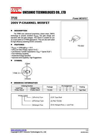
UNISONIC TECHNOLOGIES CO., LTD 7P20 Power MOSFET 200V P-CHANNEL MOSFET DESCRIPTION The 7P20 uses advanced proprietary, planar stripe, DMOS technology to provide excellent RDS(ON), low gate charge and operation with low gate voltages. This device is suitable for use as a load switch or in PWM applications. They are also well suited for high efficiency switching DC/DC converters
0.1. Size:693K fairchild semi
fqp7p20.pdf
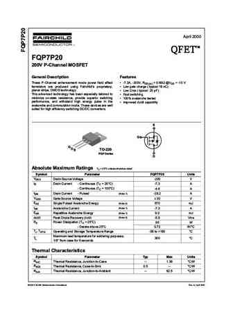
April 2000 TM QFET QFET QFET QFET 200V P-ChanneI MOSFET GeneraI Description Features These P-Channel enhancement mode power field effect -7.3A, -200V, RDS(on) = 0.69 @VGS = -10 V transistors are produced using Fairchild s proprietary, Low gate charge ( typical 19 nC) planar stripe, DMOS technology. Low Crss ( typical 25 pF) This advanced technology has bee
0.2. Size:930K fairchild semi
fqb7p20tm f085.pdf

November 2009 QFET FQB7P20TM_F085 200V P-ChanneI MOSFET GeneraI Description Features These P-Channel enhancement mode power field effect -7.3A, -200V, RDS(on) = 0.69 @VGS = -10 V transistors are produced using Fairchild s proprietary, Low gate charge ( typical 19 nC) planar stripe, DMOS technology. Low Crss ( typical 25 pF) This advanced technology has been especial
0.3. Size:731K fairchild semi
fqd7p20tf fqd7p20tm fqd7p20 fqu7p20 fqu7p20tu.pdf
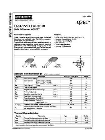
April 2000 TM QFET QFET QFET QFET FQD7P20 / FQU7P20 200V P-ChanneI MOSFET GeneraI Description Features These P-Channel enhancement mode power field effect -5.7A, -200V, RDS(on) = 0.69 @VGS = -10 V transistors are produced using Fairchild s proprietary, Low gate charge ( typical 19 nC) planar stripe, DMOS technology. Low Crss ( typical 25 pF) This advanced technolo
0.4. Size:726K fairchild semi
fqpf7p20.pdf
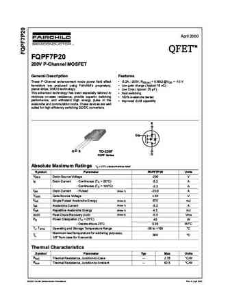
April 2000 TM QFET QFET QFET QFET 200V P-ChanneI MOSFET GeneraI Description Features These P-Channel enhancement mode power field effect -5.2A, -200V, RDS(on) = 0.69 @VGS = -10 V transistors are produced using Fairchild s proprietary, Low gate charge ( typical 19 nC) planar stripe, DMOS technology. Low Crss ( typical 25 pF) This advanced technology has be
0.5. Size:808K fairchild semi
fqb7p20 fqi7p20.pdf
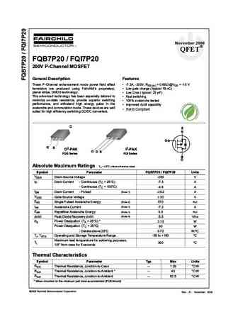
November 2008 QFET FQB7P20 / FQI7P20 200V P-ChanneI MOSFET GeneraI Description Features These P-Channel enhancement mode power field effect -7.3A, -200V, RDS(on) = 0.69 @VGS = -10 V transistors are produced using Fairchild s proprietary, Low gate charge ( typical 19 nC) planar stripe, DMOS technology. Low Crss ( typical 25 pF) This advanced technology has been espec
0.6. Size:947K onsemi
fqd7p20.pdf

Is Now Part of To learn more about ON Semiconductor, please visit our website at www.onsemi.com Please note As part of the Fairchild Semiconductor integration, some of the Fairchild orderable part numbers will need to change in order to meet ON Semiconductor s system requirements. Since the ON Semiconductor product management systems do not have the ability to manage part nomenclatur
0.7. Size:819K onsemi
fqb7p20tm f085.pdf
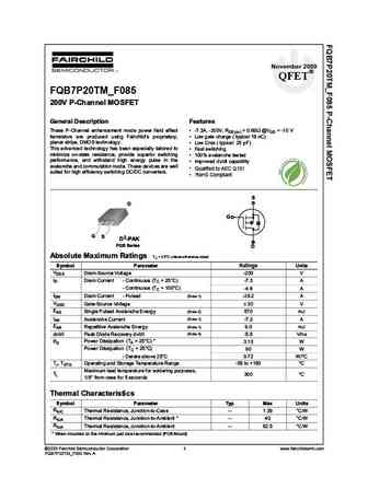
November 2009 QFET FQB7P20TM_F085 200V P-ChanneI MOSFET GeneraI Description Features These P-Channel enhancement mode power field effect -7.3A, -200V, RDS(on) = 0.69 @VGS = -10 V transistors are produced using Fairchild s proprietary, Low gate charge ( typical 19 nC) planar stripe, DMOS technology. Low Crss ( typical 25 pF) This advanced technology has been especial
0.9. Size:1324K onsemi
fqb7p20.pdf

Is Now Part of To learn more about ON Semiconductor, please visit our website at www.onsemi.com Please note As part of the Fairchild Semiconductor integration, some of the Fairchild orderable part numbers will need to change in order to meet ON Semiconductor s system requirements. Since the ON Semiconductor product management systems do not have the ability to manage part nomenclatur
0.10. Size:808K kec
kma3d7p20sa.pdf
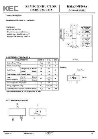
SEMICONDUCTOR KMA3D7P20SA TECHNICAL DATA P-Ch Trench MOSFET General Description It s mainly suitable for use as a load switch. E L B L FEATURES DIM MILLIMETERS _ + A 2.93 0.20 VDSS=-20V, ID=-3.7A B 1.30+0.20/-0.15 C 1.30 MAX Drain to Source on-state Resistance 2 3 D 0.40+0.15/-0.05 E 2.40+0.30/-0.20 RDS(ON)=76m (Max.) @ VGS=-4.5V 1 G 1.90 RDS(ON)=112m (Max.) @ VGS=-
0.11. Size:1411K pjsemi
pjm07p20sa.pdf
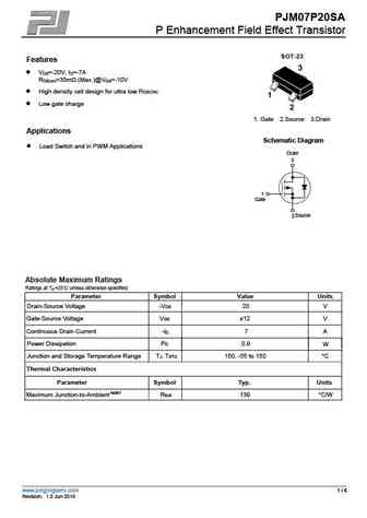
PJM07P20SA P Enhancement Field Effect Transistor SOT-23 Features VDS=-20V, ID=-7A RDS(on)=30m (Max.)@VGS=-10V High density cell design for ultra low RDS(ON) Low gate charge 1. Gate 2.Source 3.Drain Applications Schematic Diagram Load Switch and in PWM Applications Drain 3 1 Gate Source 2 Absolute Maximum Ratings Ratings at TA =25 unless otherwise speci
0.12. Size:265K inchange semiconductor
fqd7p20.pdf
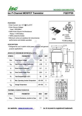
isc P-Channel MOSFET Transistor FQD7P20 FEATURES Drain Current I = -5.7A@ T =25 D C Drain Source Voltage- V = -200V(Min) DSS Static Drain-Source On-Resistance R = 0.69 (Max) DS(on) 100% avalanche tested Minimum Lot-to-Lot variations for robust device performance and reliable operation DESCRIPTION Designed for use in switch mode power supplies and general pu
Otros transistores... UF640, UF6N15, UF8010, UFZ44, URFP150, UT12N10, UT2N10, 12P10, IRF1404, UF9640, UF9Z24, UT2955, UTT120P06, UTT12P10, UTT16P10, UTT18P10, UTT25P10