MTD30N10Q8 MOSFET Equivalente. Reemplazo. Hoja de especificaciones. Principales características
Número de Parte: MTD30N10Q8
Tipo de FET: MOSFET
Polaridad de transistor: N
ESPECIFICACIONES MÁXIMAS
Pdⓘ - Máxima
disipación de potencia: 3.1 W
|Vds|ⓘ - Voltaje máximo drenador-fuente: 100 V
|Vgs|ⓘ - Voltaje máximo fuente-puerta: 20 V
|Id|ⓘ - Corriente continua
de drenaje: 6 A
Tjⓘ - Temperatura máxima de unión: 150 °C
CARACTERÍSTICAS ELÉCTRICAS
trⓘ - Tiempo
de subida: 7 nS
Cossⓘ - Capacitancia de salida: 104 pF
RDSonⓘ - Resistencia estado encendido drenaje a fuente: 0.033 Ohm
Encapsulados: SOP-8
Búsqueda de reemplazo de MTD30N10Q8 MOSFET
- Selecciónⓘ de transistores por parámetros
MTD30N10Q8 datasheet
..1. Size:341K cystek
mtd30n10q8.pdf 
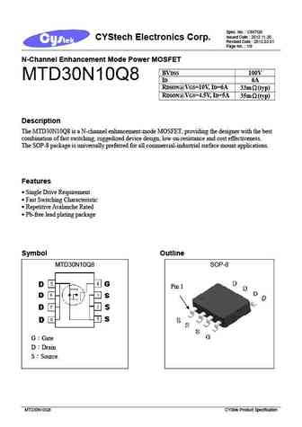
Spec. No. C887Q8 Issued Date 2012.11.30 CYStech Electronics Corp. Revised Date 2013.03.01 Page No. 1/9 N-Channel Enhancement Mode Power MOSFET BVDSS 100V MTD30N10Q8 ID 6A RDSON@VGS=10V, ID=6A 33m (typ) RDSON@VGS=4.5V, ID=5A 35m (typ) Description The MTD30N10Q8 is a N-channel enhancement-mode MOSFET, providing the designer with the best combination of fast switch
9.2. Size:184K motorola
mtd3055vl.pdf

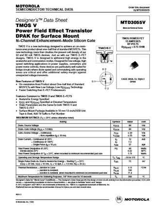
MOTOROLA Order this document SEMICONDUCTOR TECHNICAL DATA by MTD3055VL/D Designer's Data Sheet MTD3055VL TMOS V Motorola Preferred Device Power Field Effect Transistor DPAK for Surface Mount TMOS POWER FET N Channel Enhancement Mode Silicon Gate 12 AMPERES 60 VOLTS TMOS V is a new technology designed to achieve an on resis- RDS(on) = 0.18 OHM tance area product about o
9.4. Size:209K motorola
mtd3055vlrev2a.pdf
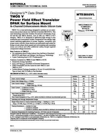
MOTOROLA Order this document SEMICONDUCTOR TECHNICAL DATA by MTD3055VL/D Designer's Data Sheet MTD3055VL TMOS V Motorola Preferred Device Power Field Effect Transistor DPAK for Surface Mount TMOS POWER FET N Channel Enhancement Mode Silicon Gate 12 AMPERES 60 VOLTS TMOS V is a new technology designed to achieve an on resis- RDS(on) = 0.18 OHM tance area product about o
9.5. Size:179K fairchild semi
mtd3055vl.pdf
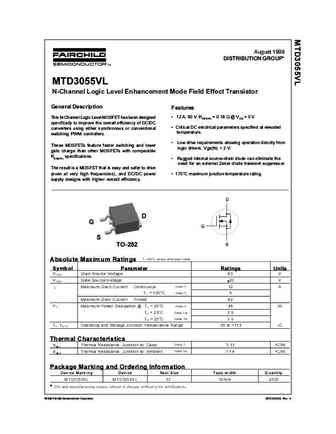
August 1999 DISTRIBUTION GROUP* MTD3055VL N-Channel Logic Level Enhancement Mode Field Effect Transistor General Description Features DS(ON) GS
9.6. Size:238K fairchild semi
mtd3055v.pdf
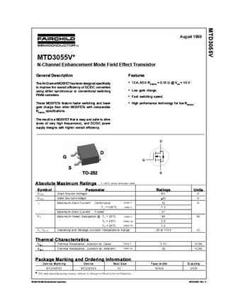
August 1999 MTD3055V* N-Channel Enhancement Mode Field Effect Transistor General Description Features 12 A, 60 V. RDS(ON) = 0.15 @ VGS = 10 V This N-Channel MOSFET has been designed specifically to improve the overall efficiency of DC/DC converters Low gate charge. using either synchronous or conventional switching PWM controllers. Fast switching speed. These MOSFETs
9.7. Size:455K onsemi
mtd3055v.pdf

Is Now Part of To learn more about ON Semiconductor, please visit our website at www.onsemi.com Please note As part of the Fairchild Semiconductor integration, some of the Fairchild orderable part numbers will need to change in order to meet ON Semiconductor s system requirements. Since the ON Semiconductor product management systems do not have the ability to manage part nomenclatur
9.8. Size:608K cystek
mtd300n20j3.pdf
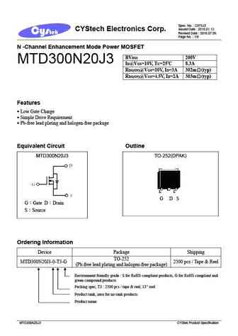
Spec. No. C875J3 Issued Date 2016.01.13 CYStech Electronics Corp. Revised Date 2016.07.06 Page No. 1/9 N -Channel Enhancement Mode Power MOSFET BVDSS 200V MTD300N20J3 ID@VGS=10V, TC=25 C 8.3A RDS(ON)@VGS=10V, ID=3A 302m (typ) RDS(ON)@VGS=4.5V, ID=2A 303m (typ) Features Low Gate Charge Simple Drive Requirement Pb-free lead plating and halogen-
9.9. Size:1449K cn vbsemi
mtd3055el.pdf
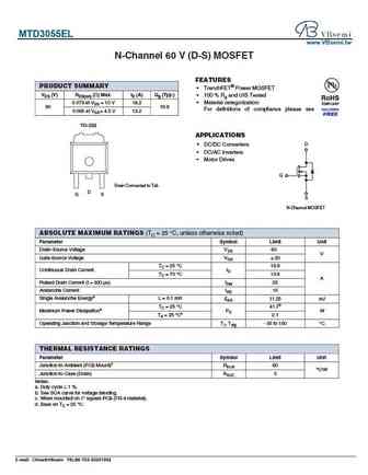
MTD3055EL www.VBsemi.tw N-Channel 60 V (D-S) MOSFET FEATURES PRODUCT SUMMARY TrenchFET Power MOSFET VDS (V) RDS(on) ( ) Max. ID (A) Qg (Typ.) 100 % Rg and UIS Tested 0.073 at VGS = 10 V 18.2 Material categorization 60 19.8 For definitions of compliance please see 0.085 at VGS = 4.5 V 13.2 TO-252 APPLICATIONS D DC/DC Converters DC/AC Inverters Moto
9.10. Size:261K inchange semiconductor
mtd300n20j3.pdf
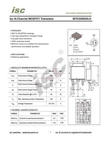
Isc N-Channel MOSFET Transistor MTD300N20J3 FEATURES With To-252(DPAK) package Low input capacitance and gate charge Low gate input resistance 100% avalanche tested Minimum Lot-to-Lot variations for robust device performance and reliable operation APPLICATIONS Switching applications ABSOLUTE MAXIMUM RATINGS(T =25 ) a SYMBOL PARAMETER VALUE UNIT V Drain-Source Vo
Otros transistores... MTC8402S6R, MTC8404V8, MTC8958G6, MTC8958Q8, MTD06N04Q8, MTD120C10KJ4, MTD120C10KQ8, MTD140P15J3, STP75NF75, MTD55N10Q8, MTDA0N10J3, MTDA0N10L3, MTDA0P10FP, MTDA4N20J3, MTDE5P10N3, MTDK1S6R, MTDK3S6R