APT10M30AVR Datasheet. Equivalente. Reemplazo. Hoja de especificaciones. Principales características
Número de Parte: APT10M30AVR 📄📄
Tipo de FET: MOSFET
Polaridad de transistor: N
ESPECIFICACIONES MÁXIMAS
Pdⓘ - Máxima disipación de potencia: 235 W
|Vds|ⓘ - Voltaje máximo drenador-fuente: 100 V
|Vgs|ⓘ - Voltaje máximo fuente-puerta: 30 V
|Id|ⓘ - Corriente continua de drenaje: 65 A
Tjⓘ - Temperatura máxima de unión: 150 °C
CARACTERÍSTICAS ELÉCTRICAS
trⓘ - Tiempo de subida: 22 nS
Cossⓘ - Capacitancia de salida: 1600 pF
RDSonⓘ - Resistencia estado encendido drenaje a fuente: 0.03 Ohm
Encapsulados: TO3
📄📄 Copiar
Búsqueda de reemplazo de APT10M30AVR MOSFET
- Selecciónⓘ de transistores por parámetros
APT10M30AVR datasheet
..1. Size:66K apt
apt10m30avr.pdf 
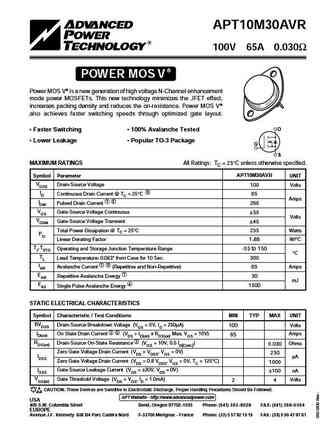
APT10M30AVR 100V 65A 0.030 POWER MOS V Power MOS V is a new generation of high voltage N-Channel enhancement mode power MOSFETs. This new technology minimizes the JFET effect, increases packing density and reduces the on-resistance. Power MOS V also achieves faster switching speeds through optimized gate layout. D Faster Switching 100% Avalanche Tested Lower Leakag
8.1. Size:117K apt
apt10m07jvfr.pdf
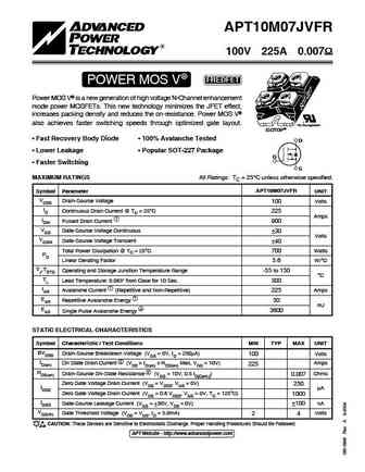
APT10M07JVFR 100V 225A 0.007 POWER MOS V FREDFET Power MOS V is a new generation of high voltage N-Channel enhancement mode power MOSFETs. This new technology minimizes the JFET effect, increases packing density and reduces the on-resistance. Power MOS V also achieves faster switching speeds through optimized gate layout. "UL Recognized" ISOTOP Fast R
8.2. Size:73K apt
apt10m07.pdf

APT10M07JVR 100V 225A 0.007 POWER MOS V Power MOS V is a new generation of high voltage N-Channel enhancement mode power MOSFETs. This new technology minimizes the JFET effect, increases packing density and reduces the on-resistance. Power MOS V also achieves faster switching speeds through optimized gate layout. "UL Recognized" ISOTOP Faster Switching 100% Avalanche
8.3. Size:38K apt
apt10m09b2vr.pdf
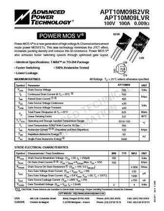
APT10M09B2VR APT10M09LVR 100V 100A 0.009W B2VR POWER MOS V T-MAX Power MOS V is a new generation of high voltage N-Channel enhancement TO-264 mode power MOSFETs. This new technology minimizes the JFET effect, increases packing density and reduces the on-resistance. Power MOS V also achieves faster switching speeds through optimized gate layout. LVR Identical Specificati
8.4. Size:73K apt
apt10m07jvr.pdf

APT10M07JVR 100V 225A 0.007 POWER MOS V Power MOS V is a new generation of high voltage N-Channel enhancement mode power MOSFETs. This new technology minimizes the JFET effect, increases packing density and reduces the on-resistance. Power MOS V also achieves faster switching speeds through optimized gate layout. "UL Recognized" ISOTOP Faster Switching 100% Avalanche
8.5. Size:146K apt
apt10m09lvfrg.pdf
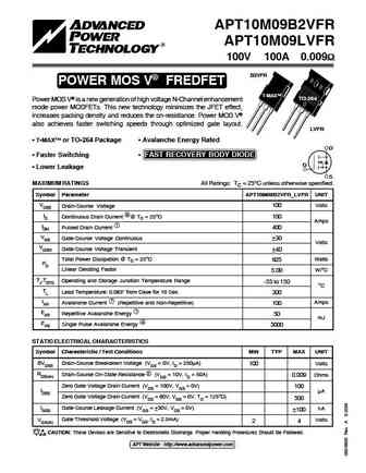
APT10M09B2VFR APT10M09LVFR 100V 100A 0.009 B2VFR POWER MOS V FREDFET T-MAX TO-264 Power MOS V is a new generation of high voltage N-Channel enhancement mode power MOSFETs. This new technology minimizes the JFET effect, increases packing density and reduces the on-resistance. Power MOS V also achieves faster switching speeds through optimized gate layou
8.6. Size:67K apt
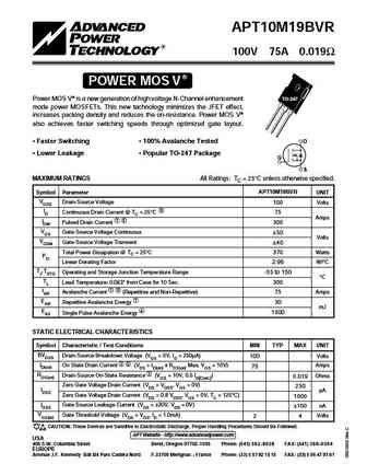
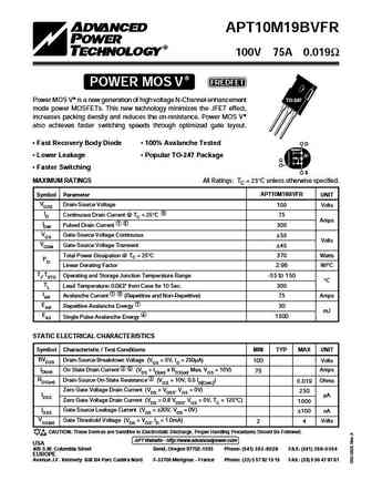
apt10m19bvr.pdf

APT10M19BVR 100V 75A 0.019 POWER MOS V Power MOS V is a new generation of high voltage N-Channel enhancement TO-247 mode power MOSFETs. This new technology minimizes the JFET effect, increases packing density and reduces the on-resistance. Power MOS V also achieves faster switching speeds through optimized gate layout. Faster Switching 100% Avalanche Tested D Lower
8.7. Size:47K apt
apt10m19bvrg.pdf
APT10M19BVR 100V 75A 0.019 POWER MOS V Power MOS V is a new generation of high voltage N-Channel enhancement TO-247 mode power MOSFETs. This new technology minimizes the JFET effect, increases packing density and reduces the on-resistance. Power MOS V also achieves faster switching speeds through optimized gate layout. Faster Switching 100% Avalanche Tested D Lower
8.8. Size:74K apt
apt10m19bvfr.pdf
APT10M19BVFR 100V 75A 0.019 POWER MOS V FREDFET TO-247 Power MOS V is a new generation of high voltage N-Channel enhancement TO-247 mode power MOSFETs. This new technology minimizes the JFET effect, increases packing density and reduces the on-resistance. Power MOS V also achieves faster switching speeds through optimized gate layout. Fast Recovery Body Diode 100% Avala
8.9. Size:70K apt
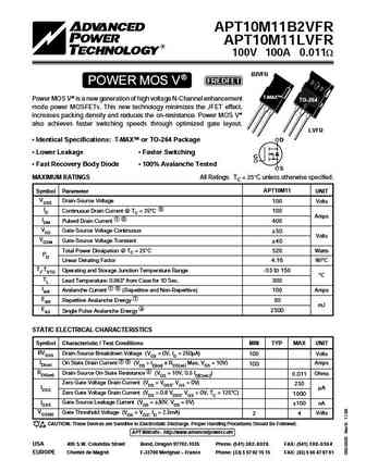
apt10m11jvr.pdf
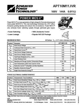
APT10M11JVR 100V 144A 0.011 POWER MOS V Power MOS V is a new generation of high voltage N-Channel enhancement mode power MOSFETs. This new technology minimizes the JFET effect, increases packing density and reduces the on-resistance. Power MOS V also achieves faster switching speeds through optimized gate layout. "UL Recognized" ISOTOP Faster Switching 100% Avalanche
8.10. Size:63K apt
apt10m11b2vr.pdf
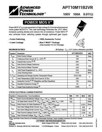
APT10M11B2VR 100V 100A 0.011 POWER MOS V T-MAX Power MOS V is a new generation of high voltage N-Channel enhancement mode power MOSFETs. This new technology minimizes the JFET effect, increases packing density and reduces the on-resistance. Power MOS V also achieves faster switching speeds through optimized gate layout. Faster Switching 100% Avalanche Tested D L
8.11. Size:39K apt
apt10m09b2vfr.pdf

APT10M09B2VFR APT10M09LVFR 100V 100A 0.009W B2VFR POWER MOS V FREDFET T-MAX Power MOS V is a new generation of high voltage N-Channel enhancement TO-264 mode power MOSFETs. This new technology minimizes the JFET effect, increases packing density and reduces the on-resistance. Power MOS V also achieves faster switching speeds through optimized gate layout. LVFR Identical
8.12. Size:70K apt
apt10m19svr.pdf
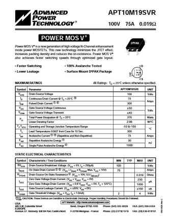
APT10M19SVR 100V 75A 0.019 POWER MOS V D3PAK Power MOS V is a new generation of high voltage N-Channel enhancement mode power MOSFETs. This new technology minimizes the JFET effect, increases packing density and reduces the on-resistance. Power MOS V also achieves faster switching speeds through optimized gate layout. D Faster Switching 100% Avalanche Tested Lower
8.13. Size:65K apt
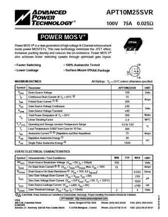
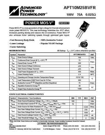
apt10m25bvr.pdf

APT10M25BVR 100V 75A 0.025 POWER MOS V Power MOS V is a new generation of high voltage N-Channel enhancement TO-247 mode power MOSFETs. This new technology minimizes the JFET effect, increases packing density and reduces the on-resistance. Power MOS V also achieves faster switching speeds through optimized gate layout. D Faster Switching 100% Avalanche Tested Lower
8.14. Size:64K apt
apt10m11b2vfrg apt10m11lvfrg.pdf
APT10M11B2VFR APT10M11LVFR 100V 100A 0.011W B2VFR POWER MOS V FREDFET T-MAX Power MOS V is a new generation of high voltage N-Channel enhancement TO-264 mode power MOSFETs. This new technology minimizes the JFET effect, increases packing density and reduces the on-resistance. Power MOS V also achieves faster switching speeds through optimized gate layout. LVFR Identical
8.15. Size:112K apt
apt10m19.pdf

APT10M19BVFR APT10M19SVFR 100V 75A 0.019 BVFR POWER MOS V FREDFET D3PAK Power MOS V is a new generation of high voltage N-Channel enhancement TO-247 mode power MOSFETs. This new technology minimizes the JFET effect, increases packing density and reduces the on-resistance. Power MOS V also achieves faster switching speeds through optimized gate layout. SV
8.16. Size:65K apt
apt10m11lvr.pdf

APT10M11LVR 100V 100A 0.011 POWER MOS V Power MOS V is a new generation of high voltage N-Channel enhancement TO-264 mode power MOSFETs. This new technology minimizes the JFET effect, increases packing density and reduces the on-resistance. Power MOS V also achieves faster switching speeds through optimized gate layout.. Faster Switching 100% Avalanche Tested D Low
8.17. Size:68K apt
apt10m25svr.pdf
APT10M25SVR 100V 75A 0.025 POWER MOS V D3PAK Power MOS V is a new generation of high voltage N-Channel enhancement mode power MOSFETs. This new technology minimizes the JFET effect, increases packing density and reduces the on-resistance. Power MOS V also achieves faster switching speeds through optimized gate layout. D Faster Switching 100% Avalanche Tested Lower
8.18. Size:69K apt
apt10m25.pdf
APT10M25BVFR 100V 75A 0.025 POWER MOS V FREDFET Power MOS V is a new generation of high voltage N-Channel enhancement TO-247 mode power MOSFETs. This new technology minimizes the JFET effect, increases packing density and reduces the on-resistance. Power MOS V also achieves faster switching speeds through optimized gate layout. Fast Recovery Body Diode 100% Avalanche Tes
8.19. Size:69K apt
apt10m25bvfr.pdf

APT10M25BVFR 100V 75A 0.025 POWER MOS V FREDFET Power MOS V is a new generation of high voltage N-Channel enhancement TO-247 mode power MOSFETs. This new technology minimizes the JFET effect, increases packing density and reduces the on-resistance. Power MOS V also achieves faster switching speeds through optimized gate layout. Fast Recovery Body Diode 100% Avalanche Tes
8.20. Size:118K apt
apt10m11jvfr.pdf
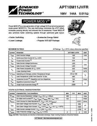
APT10M11JVFR 100V 144A 0.011 POWER MOS V Power MOS V is a new generation of high voltage N-Channel enhancement mode power MOSFETs. This new technology minimizes the JFET effect, increases packing density and reduces the on-resistance. Power MOS V also achieves faster switching speeds through optimized gate layout. "UL Recognized" ISOTOP Faster Switchi
8.21. Size:117K apt
apt10m19bvfrg apt10m19svfr apt10m19svfrg.pdf
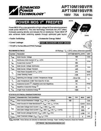
APT10M19BVFR APT10M19SVFR 100V 75A 0.019 BVFR POWER MOS V FREDFET D3PAK Power MOS V is a new generation of high voltage N-Channel enhancement TO-247 mode power MOSFETs. This new technology minimizes the JFET effect, increases packing density and reduces the on-resistance. Power MOS V also achieves faster switching speeds through optimized gate layout. SV
8.22. Size:376K inchange semiconductor
apt10m19bvr.pdf
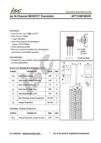
isc N-Channel MOSFET Transistor APT10M19BVR FEATURES Drain Current I =75A@ T =25 D C Drain Source Voltage- V =100V(Min) DSS Static Drain-Source On-Resistance R =0.019 (Max) DS(on) 100% avalanche tested Minimum Lot-to-Lot variations for robust device performance and reliable operation DESCRIPTION Designed for use in switch mode power supplies and general pur
8.23. Size:255K inchange semiconductor
apt10m09lvfr.pdf
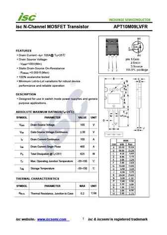
isc N-Channel MOSFET Transistor APT10M09LVFR FEATURES Drain Current I = 100A@ T =25 D C Drain Source Voltage- V =100V(Min) DSS Static Drain-Source On-Resistance R =0.009 (Max) DS(on) 100% avalanche tested Minimum Lot-to-Lot variations for robust device performance and reliable operation DESCRIPTION Designed for use in switch mode power supplies and general
8.24. Size:376K inchange semiconductor
apt10m09b2vfr.pdf

isc N-Channel MOSFET Transistor APT10M09B2VFR FEATURES Drain Current I = 100A@ T =25 D C Drain Source Voltage- V =100V(Min) DSS Static Drain-Source On-Resistance R =0.009 (Max) DS(on) 100% avalanche tested Minimum Lot-to-Lot variations for robust device performance and reliable operation DESCRIPTION Designed for use in switch mode power supplies and general
8.25. Size:375K inchange semiconductor
apt10m25bvr.pdf

isc N-Channel MOSFET Transistor APT10M25BVR FEATURES Drain Current I =75A@ T =25 D C Drain Source Voltage- V =100V(Min) DSS Static Drain-Source On-Resistance R =0.025 (Max) DS(on) 100% avalanche tested Minimum Lot-to-Lot variations for robust device performance and reliable operation DESCRIPTION Designed for use in switch mode power supplies and general pur
Otros transistores... APT10086BLC, APT10086SLC, APT10090BFLL, APT10090SFLL, APT10090BLL, APT10090SLL, APT10M09B2VFR, APT10M09B2VR, 50N06, APT11N80BC3, APT11N80KC3, APT1201R2BLL, APT1201R2SLL, APT1201R4BLL, APT1201R4SLL, APT1201R5BVFR, APT1201R5SVFR
