APT10M30AVR Specs and Replacement
Type Designator: APT10M30AVR
Type of Transistor: MOSFET
Type of Control Channel: N-Channel
Absolute Maximum Ratings
Pd ⓘ
- Maximum Power Dissipation: 235 W
|Vds|ⓘ - Maximum Drain-Source Voltage: 100 V
|Vgs|ⓘ - Maximum Gate-Source Voltage: 30 V
|Id| ⓘ - Maximum Drain Current: 65 A
Tj ⓘ - Maximum Junction Temperature: 150 °C
Electrical Characteristics
tr ⓘ - Rise Time: 22 nS
Cossⓘ -
Output Capacitance: 1600 pF
RDSonⓘ - Maximum Drain-Source On-State Resistance: 0.03 Ohm
Package: TO3
- MOSFET ⓘ Cross-Reference Search
APT10M30AVR datasheet
..1. Size:66K apt
apt10m30avr.pdf 
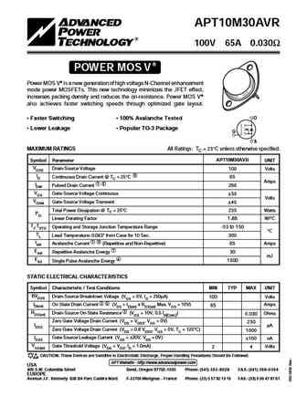
APT10M30AVR 100V 65A 0.030 POWER MOS V Power MOS V is a new generation of high voltage N-Channel enhancement mode power MOSFETs. This new technology minimizes the JFET effect, increases packing density and reduces the on-resistance. Power MOS V also achieves faster switching speeds through optimized gate layout. D Faster Switching 100% Avalanche Tested Lower Leakag... See More ⇒
8.1. Size:117K apt
apt10m07jvfr.pdf
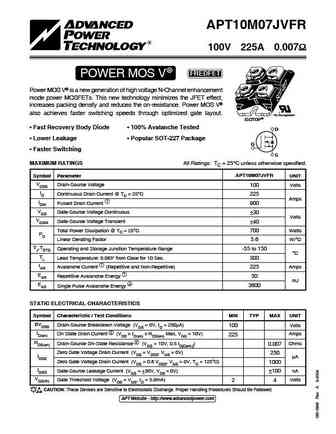
APT10M07JVFR 100V 225A 0.007 POWER MOS V FREDFET Power MOS V is a new generation of high voltage N-Channel enhancement mode power MOSFETs. This new technology minimizes the JFET effect, increases packing density and reduces the on-resistance. Power MOS V also achieves faster switching speeds through optimized gate layout. "UL Recognized" ISOTOP Fast R... See More ⇒
8.2. Size:73K apt
apt10m07.pdf

APT10M07JVR 100V 225A 0.007 POWER MOS V Power MOS V is a new generation of high voltage N-Channel enhancement mode power MOSFETs. This new technology minimizes the JFET effect, increases packing density and reduces the on-resistance. Power MOS V also achieves faster switching speeds through optimized gate layout. "UL Recognized" ISOTOP Faster Switching 100% Avalanche... See More ⇒
8.3. Size:38K apt
apt10m09b2vr.pdf
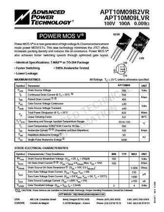
APT10M09B2VR APT10M09LVR 100V 100A 0.009W B2VR POWER MOS V T-MAX Power MOS V is a new generation of high voltage N-Channel enhancement TO-264 mode power MOSFETs. This new technology minimizes the JFET effect, increases packing density and reduces the on-resistance. Power MOS V also achieves faster switching speeds through optimized gate layout. LVR Identical Specificati... See More ⇒
8.4. Size:73K apt
apt10m07jvr.pdf

APT10M07JVR 100V 225A 0.007 POWER MOS V Power MOS V is a new generation of high voltage N-Channel enhancement mode power MOSFETs. This new technology minimizes the JFET effect, increases packing density and reduces the on-resistance. Power MOS V also achieves faster switching speeds through optimized gate layout. "UL Recognized" ISOTOP Faster Switching 100% Avalanche... See More ⇒
8.5. Size:146K apt
apt10m09lvfrg.pdf
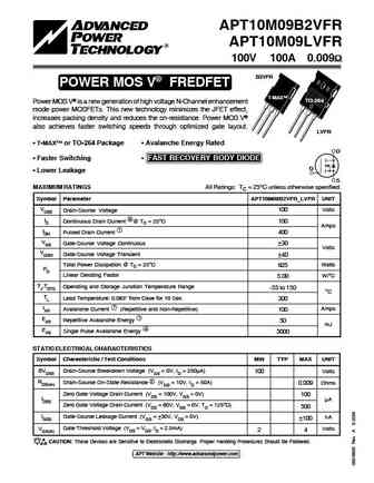
APT10M09B2VFR APT10M09LVFR 100V 100A 0.009 B2VFR POWER MOS V FREDFET T-MAX TO-264 Power MOS V is a new generation of high voltage N-Channel enhancement mode power MOSFETs. This new technology minimizes the JFET effect, increases packing density and reduces the on-resistance. Power MOS V also achieves faster switching speeds through optimized gate layou... See More ⇒
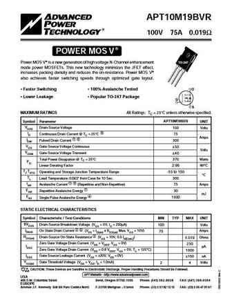
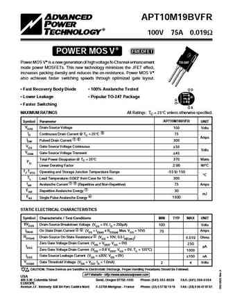
8.6. Size:67K apt
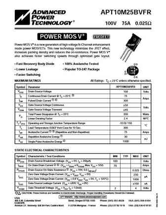
apt10m19bvr.pdf

APT10M19BVR 100V 75A 0.019 POWER MOS V Power MOS V is a new generation of high voltage N-Channel enhancement TO-247 mode power MOSFETs. This new technology minimizes the JFET effect, increases packing density and reduces the on-resistance. Power MOS V also achieves faster switching speeds through optimized gate layout. Faster Switching 100% Avalanche Tested D Lower ... See More ⇒
8.7. Size:47K apt
apt10m19bvrg.pdf
APT10M19BVR 100V 75A 0.019 POWER MOS V Power MOS V is a new generation of high voltage N-Channel enhancement TO-247 mode power MOSFETs. This new technology minimizes the JFET effect, increases packing density and reduces the on-resistance. Power MOS V also achieves faster switching speeds through optimized gate layout. Faster Switching 100% Avalanche Tested D Lower ... See More ⇒
8.8. Size:74K apt
apt10m19bvfr.pdf
APT10M19BVFR 100V 75A 0.019 POWER MOS V FREDFET TO-247 Power MOS V is a new generation of high voltage N-Channel enhancement TO-247 mode power MOSFETs. This new technology minimizes the JFET effect, increases packing density and reduces the on-resistance. Power MOS V also achieves faster switching speeds through optimized gate layout. Fast Recovery Body Diode 100% Avala... See More ⇒
8.9. Size:70K apt
apt10m11jvr.pdf
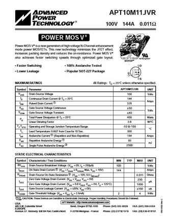
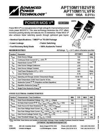
APT10M11JVR 100V 144A 0.011 POWER MOS V Power MOS V is a new generation of high voltage N-Channel enhancement mode power MOSFETs. This new technology minimizes the JFET effect, increases packing density and reduces the on-resistance. Power MOS V also achieves faster switching speeds through optimized gate layout. "UL Recognized" ISOTOP Faster Switching 100% Avalanche... See More ⇒
8.10. Size:63K apt
apt10m11b2vr.pdf
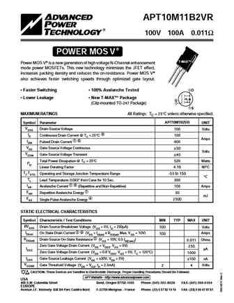
APT10M11B2VR 100V 100A 0.011 POWER MOS V T-MAX Power MOS V is a new generation of high voltage N-Channel enhancement mode power MOSFETs. This new technology minimizes the JFET effect, increases packing density and reduces the on-resistance. Power MOS V also achieves faster switching speeds through optimized gate layout. Faster Switching 100% Avalanche Tested D L... See More ⇒
8.11. Size:39K apt
apt10m09b2vfr.pdf

APT10M09B2VFR APT10M09LVFR 100V 100A 0.009W B2VFR POWER MOS V FREDFET T-MAX Power MOS V is a new generation of high voltage N-Channel enhancement TO-264 mode power MOSFETs. This new technology minimizes the JFET effect, increases packing density and reduces the on-resistance. Power MOS V also achieves faster switching speeds through optimized gate layout. LVFR Identical... See More ⇒
8.12. Size:70K apt
apt10m19svr.pdf
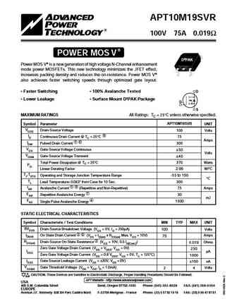
APT10M19SVR 100V 75A 0.019 POWER MOS V D3PAK Power MOS V is a new generation of high voltage N-Channel enhancement mode power MOSFETs. This new technology minimizes the JFET effect, increases packing density and reduces the on-resistance. Power MOS V also achieves faster switching speeds through optimized gate layout. D Faster Switching 100% Avalanche Tested Lower... See More ⇒
8.13. Size:65K apt
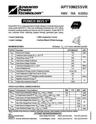
apt10m25bvr.pdf

APT10M25BVR 100V 75A 0.025 POWER MOS V Power MOS V is a new generation of high voltage N-Channel enhancement TO-247 mode power MOSFETs. This new technology minimizes the JFET effect, increases packing density and reduces the on-resistance. Power MOS V also achieves faster switching speeds through optimized gate layout. D Faster Switching 100% Avalanche Tested Lower... See More ⇒
8.14. Size:64K apt
apt10m11b2vfrg apt10m11lvfrg.pdf
APT10M11B2VFR APT10M11LVFR 100V 100A 0.011W B2VFR POWER MOS V FREDFET T-MAX Power MOS V is a new generation of high voltage N-Channel enhancement TO-264 mode power MOSFETs. This new technology minimizes the JFET effect, increases packing density and reduces the on-resistance. Power MOS V also achieves faster switching speeds through optimized gate layout. LVFR Identical... See More ⇒
8.15. Size:112K apt
apt10m19.pdf

APT10M19BVFR APT10M19SVFR 100V 75A 0.019 BVFR POWER MOS V FREDFET D3PAK Power MOS V is a new generation of high voltage N-Channel enhancement TO-247 mode power MOSFETs. This new technology minimizes the JFET effect, increases packing density and reduces the on-resistance. Power MOS V also achieves faster switching speeds through optimized gate layout. SV... See More ⇒
8.16. Size:65K apt
apt10m11lvr.pdf

APT10M11LVR 100V 100A 0.011 POWER MOS V Power MOS V is a new generation of high voltage N-Channel enhancement TO-264 mode power MOSFETs. This new technology minimizes the JFET effect, increases packing density and reduces the on-resistance. Power MOS V also achieves faster switching speeds through optimized gate layout.. Faster Switching 100% Avalanche Tested D Low... See More ⇒
8.17. Size:68K apt
apt10m25svr.pdf
APT10M25SVR 100V 75A 0.025 POWER MOS V D3PAK Power MOS V is a new generation of high voltage N-Channel enhancement mode power MOSFETs. This new technology minimizes the JFET effect, increases packing density and reduces the on-resistance. Power MOS V also achieves faster switching speeds through optimized gate layout. D Faster Switching 100% Avalanche Tested Lower... See More ⇒
8.18. Size:69K apt
apt10m25.pdf
APT10M25BVFR 100V 75A 0.025 POWER MOS V FREDFET Power MOS V is a new generation of high voltage N-Channel enhancement TO-247 mode power MOSFETs. This new technology minimizes the JFET effect, increases packing density and reduces the on-resistance. Power MOS V also achieves faster switching speeds through optimized gate layout. Fast Recovery Body Diode 100% Avalanche Tes... See More ⇒
8.19. Size:69K apt
apt10m25bvfr.pdf

APT10M25BVFR 100V 75A 0.025 POWER MOS V FREDFET Power MOS V is a new generation of high voltage N-Channel enhancement TO-247 mode power MOSFETs. This new technology minimizes the JFET effect, increases packing density and reduces the on-resistance. Power MOS V also achieves faster switching speeds through optimized gate layout. Fast Recovery Body Diode 100% Avalanche Tes... See More ⇒
8.20. Size:118K apt
apt10m11jvfr.pdf
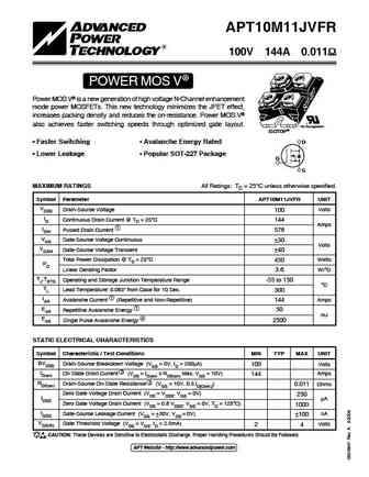
APT10M11JVFR 100V 144A 0.011 POWER MOS V Power MOS V is a new generation of high voltage N-Channel enhancement mode power MOSFETs. This new technology minimizes the JFET effect, increases packing density and reduces the on-resistance. Power MOS V also achieves faster switching speeds through optimized gate layout. "UL Recognized" ISOTOP Faster Switchi... See More ⇒
8.21. Size:117K apt
apt10m19bvfrg apt10m19svfr apt10m19svfrg.pdf
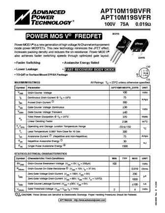
APT10M19BVFR APT10M19SVFR 100V 75A 0.019 BVFR POWER MOS V FREDFET D3PAK Power MOS V is a new generation of high voltage N-Channel enhancement TO-247 mode power MOSFETs. This new technology minimizes the JFET effect, increases packing density and reduces the on-resistance. Power MOS V also achieves faster switching speeds through optimized gate layout. SV... See More ⇒
8.22. Size:376K inchange semiconductor
apt10m19bvr.pdf
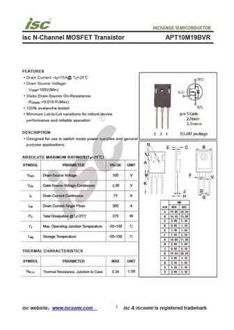
isc N-Channel MOSFET Transistor APT10M19BVR FEATURES Drain Current I =75A@ T =25 D C Drain Source Voltage- V =100V(Min) DSS Static Drain-Source On-Resistance R =0.019 (Max) DS(on) 100% avalanche tested Minimum Lot-to-Lot variations for robust device performance and reliable operation DESCRIPTION Designed for use in switch mode power supplies and general pur... See More ⇒
8.23. Size:255K inchange semiconductor
apt10m09lvfr.pdf
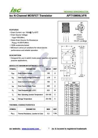
isc N-Channel MOSFET Transistor APT10M09LVFR FEATURES Drain Current I = 100A@ T =25 D C Drain Source Voltage- V =100V(Min) DSS Static Drain-Source On-Resistance R =0.009 (Max) DS(on) 100% avalanche tested Minimum Lot-to-Lot variations for robust device performance and reliable operation DESCRIPTION Designed for use in switch mode power supplies and general ... See More ⇒
8.24. Size:376K inchange semiconductor
apt10m09b2vfr.pdf

isc N-Channel MOSFET Transistor APT10M09B2VFR FEATURES Drain Current I = 100A@ T =25 D C Drain Source Voltage- V =100V(Min) DSS Static Drain-Source On-Resistance R =0.009 (Max) DS(on) 100% avalanche tested Minimum Lot-to-Lot variations for robust device performance and reliable operation DESCRIPTION Designed for use in switch mode power supplies and general ... See More ⇒
8.25. Size:375K inchange semiconductor
apt10m25bvr.pdf

isc N-Channel MOSFET Transistor APT10M25BVR FEATURES Drain Current I =75A@ T =25 D C Drain Source Voltage- V =100V(Min) DSS Static Drain-Source On-Resistance R =0.025 (Max) DS(on) 100% avalanche tested Minimum Lot-to-Lot variations for robust device performance and reliable operation DESCRIPTION Designed for use in switch mode power supplies and general pur... See More ⇒
Detailed specifications: APT10086BLC, APT10086SLC, APT10090BFLL, APT10090SFLL, APT10090BLL, APT10090SLL, APT10M09B2VFR, APT10M09B2VR, IRFP460, APT11N80BC3, APT11N80KC3, APT1201R2BLL, APT1201R2SLL, APT1201R4BLL, APT1201R4SLL, APT1201R5BVFR, APT1201R5SVFR
Keywords - APT10M30AVR MOSFET specs
APT10M30AVR cross reference
APT10M30AVR equivalent finder
APT10M30AVR pdf lookup
APT10M30AVR substitution
APT10M30AVR replacement
Learn how to find the right MOSFET substitute. A guide to cross-reference, check specs and replace MOSFETs in your circuits.
