FDMS015N04B MOSFET Equivalente. Reemplazo. Hoja de especificaciones. Principales características
Número de Parte: FDMS015N04B
Tipo de FET: MOSFET
Polaridad de transistor: N
ESPECIFICACIONES MÁXIMAS
Pdⓘ - Máxima
disipación de potencia: 2.5 W
|Vds|ⓘ - Voltaje máximo drenador-fuente: 40 V
|Vgs|ⓘ - Voltaje máximo fuente-puerta: 20 V
|Id|ⓘ - Corriente continua
de drenaje: 31.3 A
Tjⓘ - Temperatura máxima de unión: 150 °C
CARACTERÍSTICAS ELÉCTRICAS
trⓘ - Tiempo
de subida: 24 nS
Cossⓘ - Capacitancia de salida: 2795 pF
RDSonⓘ - Resistencia estado encendido drenaje a fuente: 0.0015 Ohm
Encapsulados: PQFN5X6
Búsqueda de reemplazo de FDMS015N04B MOSFET
- Selecciónⓘ de transistores por parámetros
FDMS015N04B datasheet
..1. Size:1373K fairchild semi
fdms015n04b.pdf 

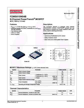
November 2013 FDMS015N04B N-Channel PowerTrench MOSFET 40 V, 100 A, 1.5 m Features Description RDS(on) = 1.13 m (Typ.) @ VGS = 10 V, ID = 50 A This N-Channel MOSFET is produced using Fairchild Advanced Package and Silicon Combination for Low RDS(on) Semiconductor s advance PowerTrench process that has and High Efficiency been tailored to minimize the on-state resistance
..2. Size:780K onsemi
fdms015n04b.pdf 

Is Now Part of To learn more about ON Semiconductor, please visit our website at www.onsemi.com Please note As part of the Fairchild Semiconductor integration, some of the Fairchild orderable part numbers will need to change in order to meet ON Semiconductor s system requirements. Since the ON Semiconductor product management systems do not have the ability to manage part nomenclatur
9.1. Size:970K 1
fdms039n08b.pdf 

ON Semiconductor Is Now To learn more about onsemi , please visit our website at www.onsemi.com onsemi and and other names, marks, and brands are registered and/or common law trademarks of Semiconductor Components Industries, LLC dba onsemi or its affiliates and/or subsidiaries in the United States and/or other countries. onsemi owns the rights to a number of patents, trademarks,
9.2. Size:1386K fairchild semi
fdms037n08b.pdf 

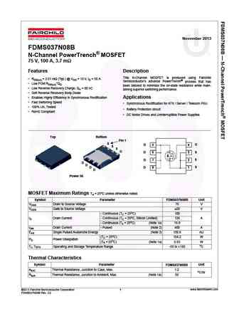
November 2013 FDMS037N08B N-Channel PowerTrench MOSFET 75 V, 100 A, 3.7 m Features Description This N-Channel MOSFET is produced using Fairchild RDS(on) = 3.01 m (Typ.) @ VGS = 10 V, ID = 50 A Semiconductor s advance PowerTrench process that has Low FOM RDS(on)*QG been tailored to minimize the on-state resistance while main- Low Reverse Recovery Charge, Qrr = 80
9.3. Size:288K fairchild semi
fdms0306as.pdf 

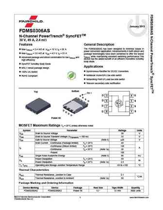
January 2015 FDMS0306AS N-Channel PowerTrench SyncFETTM 30 V, 49 A, 2.4 m Features General Description The FDMS0306AS has been designed to minimize losses in Max rDS(on) = 2.4 m at VGS = 10 V, ID = 26 A power conversion application. Advancements in both silicon and Max rDS(on) = 3.0 m at VGS = 4.5 V, ID = 23 A package technologies have been combined to offer the lowest rD
9.4. Size:454K fairchild semi
fdms0310s.pdf 

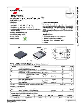
January 2015 FDMS0310S N-Channel PowerTrench SyncFETTM 30 V, 42 A, 4 m Features General Description The FDMS0310S has been designed to minimize losses in Max rDS(on) = 4.0 m at VGS = 10 V, ID = 18 A power conversion application. Advancements in both silicon and Max rDS(on) = 5.2 m at VGS = 4.5 V, ID = 14 A package technologies have been combined to offer the lowest Advan
9.5. Size:1403K fairchild semi
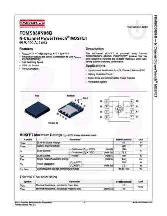
fdms030n06b.pdf 

November 2013 FDMS030N06B N-Channel PowerTrench MOSFET 60 V, 100 A, 3 m Features Description RDS(on) = 2.4 m (Typ.) @ VGS = 10 V, ID = 50 A This N-Channel MOSFET is produced using Fairchild Advanced Package and Silicon Combination for Low RDS(on) Semiconductor s advance PowerTrench process that has and High Efficiency been tailored to minimize the on-state resistance wh
9.6. Size:270K fairchild semi
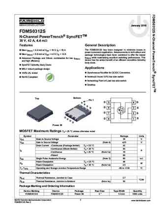
fdms0312s.pdf 

January 2010 FDMS0312S N-Channel PowerTrench SyncFETTM 30 V, 42 A, 4.4 m Features General Description The FDMS0312S has been designed to minimize losses in Max rDS(on) = 4.4 m at VGS = 10 V, ID = 18 A power conversion application. Advancements in both silicon and Max rDS(on) = 5.8 m at VGS = 4.5 V, ID = 14 A package technologies have been combined to offer the lowest
9.7. Size:195K fairchild semi
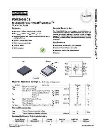
fdms0308cs.pdf 

August 2010 FDMS0308CS N-Channel PowerTrench SyncFETTM 30 V, 42 A, 3 m Features General Description The FDMS0308CS has been designed to minimize losses in Max rDS(on) = 3.0 m at VGS = 10 V, ID = 21 A power conversion application. Advancements in both silicon and Max rDS(on) = 3.5 m at VGS = 4.5 V, ID = 17 A package technologies have been combined to offer the lowest Advanc
9.8. Size:294K fairchild semi
fdms0308as.pdf 

October 2014 FDMS0308AS N-Channel PowerTrench SyncFETTM 30 V, 49 A, 2.8 m Features General Description The FDMS0308AS has been designed to minimize losses in Max rDS(on) = 2.8 m at VGS = 10 V, ID = 24 A power conversion application. Advancements in both silicon and Max rDS(on) = 3.5 m at VGS = 4.5 V, ID = 21 A package technologies have been combined to offer the lowest rD
9.9. Size:1367K fairchild semi
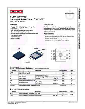
fdms039n08b.pdf 

November 2013 FDMS039N08B N-Channel PowerTrench MOSFET 80 V, 100 A, 3.9 m Features Description RDS(on) = 3.2 m (Typ.) @ VGS = 10 V, ID = 50 A This N-Channel MOSFET is produced using Fairchild Semicon- ductor s advance PowerTrench process that has been tailored Low FOM RDS(on) *QG to minimize the on-state resistance while maintaining superior Low Reverse Recovery
9.10. Size:309K fairchild semi
fdms0309as.pdf 

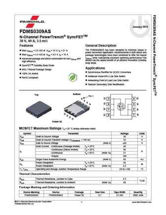
January 2015 FDMS0309AS N-Channel PowerTrench SyncFETTM 30 V, 49 A, 3.5 m Features General Description The FDMS0309AS has been designed to minimize losses in Max rDS(on) = 3.5 m at VGS = 10 V, ID = 21 A power conversion application. Advancements in both silicon and Max rDS(on) = 4.3 m at VGS = 4.5 V, ID = 19 A package technologies have been combined to offer the lowest rD
9.11. Size:272K fairchild semi
fdms0300s.pdf 

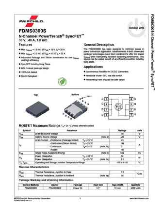
October 2014 FDMS0300S N-Channel PowerTrench SyncFET 30 V, 49 A, 1.8 m Features General Description The FDMS0300S has been designed to minimize losses in Max rDS(on) = 1.8 m at VGS = 10 V, ID = 30 A power conversion application. Advancements in both silicon and Max rDS(on) = 2.0 m at VGS = 4.5 V, ID = 25 A package technologies have been combined to offer the lowest
9.12. Size:337K fairchild semi
fdms0310as.pdf 

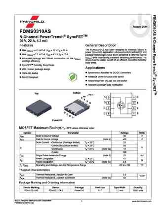
August 2014 FDMS0310AS N-Channel PowerTrench SyncFETTM 30 V, 22 A, 4.3 m Features General Description The FDMS0310AS has been designed to minimize losses in Max rDS(on) = 4.3 m at VGS = 10 V, ID = 19 A power conversion application. Advancements in both silicon and Max rDS(on) = 5.2 m at VGS = 4.5 V, ID = 17 A package technologies have been combined to offer the lowest A
9.13. Size:305K fairchild semi
fdms0312as.pdf 

October 2014 FDMS0312AS N-Channel PowerTrench SyncFETTM 30 V, 22 A, 5.0 m Features General Description The FDMS0312AS has been designed to minimize losses in Max rDS(on) = 5.0 m at VGS = 10 V, ID = 18 A power conversion application. Advancements in both silicon and Max rDS(on) = 6.2 m at VGS = 4.5 V, ID = 16 A package technologies have been combined to offer the lowest A
9.14. Size:468K fairchild semi
fdms0302s.pdf 

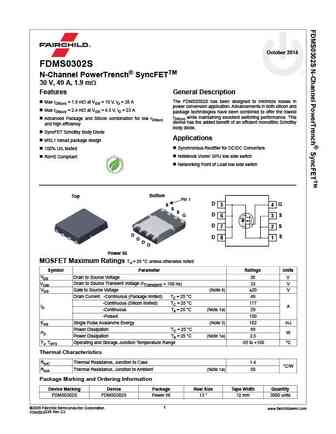
October 2014 FDMS0302S N-Channel PowerTrench SyncFETTM 30 V, 49 A, 1.9 m Features General Description The FDMS0302S has been designed to minimize losses in Max rDS(on) = 1.9 m at VGS = 10 V, ID = 28 A power conversion application. Advancements in both silicon and Max rDS(on) = 2.4 m at VGS = 4.5 V, ID = 23 A package technologies have been combined to offer the lowest
9.15. Size:402K onsemi
fdms0308as.pdf 

Is Now Part of To learn more about ON Semiconductor, please visit our website at www.onsemi.com Please note As part of the Fairchild Semiconductor integration, some of the Fairchild orderable part numbers will need to change in order to meet ON Semiconductor s system requirements. Since the ON Semiconductor product management systems do not have the ability to manage part nomenclatur
9.16. Size:506K onsemi
fdms007n08lc.pdf 

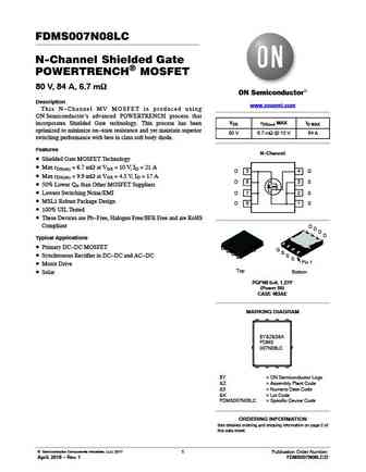
FDMS007N08LC N-Channel Shielded Gate POWERTRENCH) MOSFET 80 V, 84 A, 6.7 mW Description www.onsemi.com This N-Channel MV MOSFET is produced using ON Semiconductor s advanced POWERTRENCH process that VDS rDS(on) MAX ID MAX incorporates Shielded Gate technology. This process has been optimized to minimize on-state resistance and yet maintain superior 80 V 6.7 mW @ 10 V 84 A switchin
Otros transistores... FDMA8878
, FDMS86101A
, FDPC8011S
, HUF75639SF085A
, FDMS3620S
, FDMS86300DC
, FCPF400N60
, FDD86540
, IRFZ48N
, FDD390N15ALZ
, FDMA7628
, FDMC86248
, FDPC8013S
, FDP039N08B
, FDME820NZT
, FDS86540
, FDPF18N20FTG
.
History: IRFS4227
