2N7002KB Datasheet. Equivalente. Reemplazo. Hoja de especificaciones. Principales características
Número de Parte: 2N7002KB 📄📄
Tipo de FET: MOSFET
Polaridad de transistor: N
ESPECIFICACIONES MÁXIMAS
Pdⓘ - Máxima disipación de potencia: 0.63 W
|Vds|ⓘ - Voltaje máximo drenador-fuente: 60 V
|Vgs|ⓘ - Voltaje máximo fuente-puerta: 20 V
|Id|ⓘ - Corriente continua de drenaje: 0.3 A
Tjⓘ - Temperatura máxima de unión: 150 °C
CARACTERÍSTICAS ELÉCTRICAS
Cossⓘ - Capacitancia de salida: 16.6 pF
RDSonⓘ - Resistencia estado encendido drenaje a fuente: 2 Ohm
Encapsulados: SOT23
📄📄 Copiar
Búsqueda de reemplazo de 2N7002KB MOSFET
- Selecciónⓘ de transistores por parámetros
2N7002KB datasheet
2n7002kb.pdf
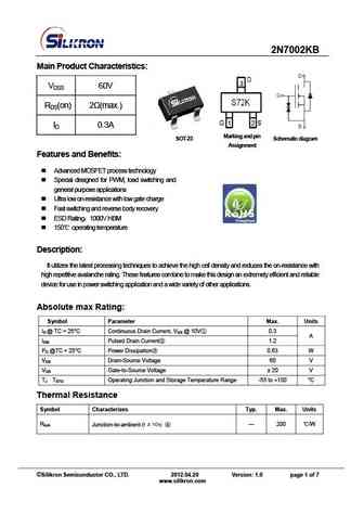
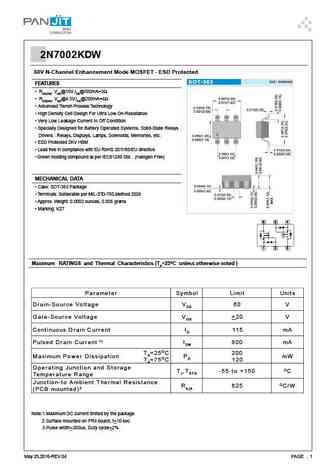
2N7002KB Main Product Characteristics VDSS 60V RDS(on) 2 (max.) ID 0.3A Marking and pin SOT-23 Schema t ic diag r am Assignment Features and Benefits Advanced MOSFET process technology Special designed for PWM, load switching and general purpose applications Ultra low on-resistance with low gate charge Fast switching and reverse body recovery
2n7002kb.pdf
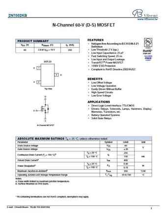
2N7002KB www.VBsemi.tw N-Channel 60-V (D-S) MOSFET FEATURES PRODUCT SUMMARY Halogen-free According to IEC 61249-2-21 VDS (V) RDS(on) ( )ID (mA) Definition 2.8 at VGS = 10 V 60 250 Low Threshold 2 V (typ.) Low Input Capacitance 25 pF Fast Switching Speed 25 ns Low Input and Output Leakage SOT-23 TrenchFET Power MOSFET 1200V ESD Protection G 1
2n7002ka.pdf
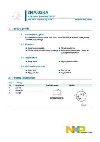
2N7002KA N-channel TrenchMOS FET Rev. 03 25 February 2008 Product data sheet 1. Product profile 1.1 General description N-channel enhancement mode Field-Effect Transistor (FET) in a plastic package using TrenchMOS technology. 1.2 Features Logic level compatible Very fast switching Subminiature surface-mounted package Gate-source ElectroStatic Discharge (ESD) protection diodes 1
2n7002kw.pdf
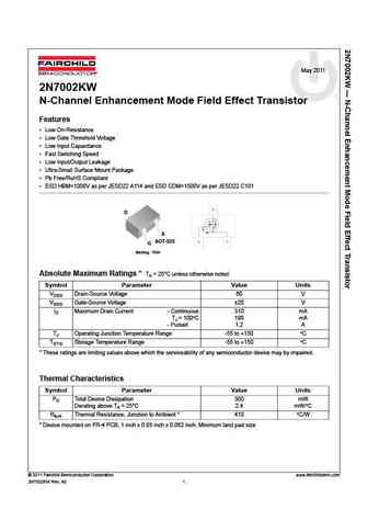
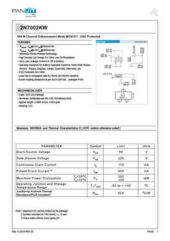
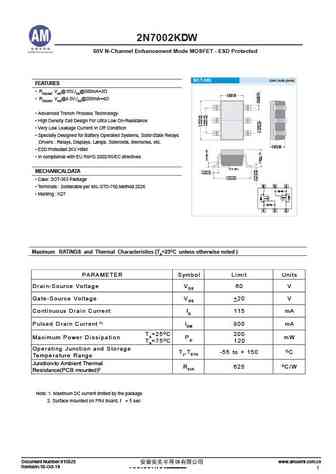
May 2011 2N7002KW N-Channel Enhancement Mode Field Effect Transistor Features Low On-Resistance Low Gate Threshold Voltage Low Input Capacitance Fast Switching Speed Low Input/Output Leakage Ultra-Small Surface Mount Package Pb Free/RoHS Compliant ESD HBM=1000V as per JESD22 A114 and ESD CDM=1500V as per JESD22 C101 D S SOT-323 G Marking 7KW Ab
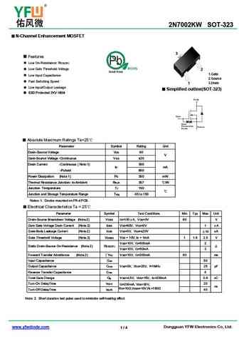
2n7002k.pdf
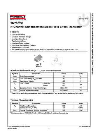
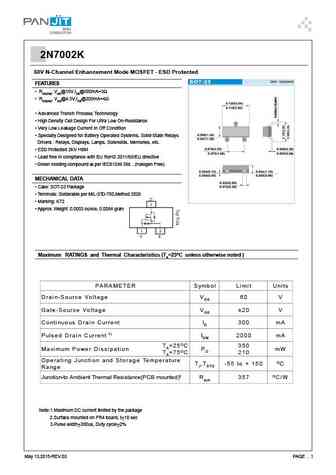
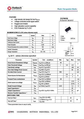
January 2012 2N7002K N-Channel Enhancement Mode Field Effect Transistor Features Low On-Resistance Low Gate Threshold Voltage Low Input Capacitance Fast Switching Speed Low Input/Output Leakage Ultra-Small Surface Mount Package Pb Free/RoHS Compliant ESD HBM=2000V (Typical 3000V) as per JESD22 A114 and ESD CDM=2000V as per JESD22 C101 D S G SOT-23
2n7002k.pdf
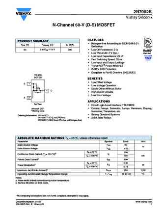
2N7002K Vishay Siliconix N-Channel 60-V (D-S) MOSFET FEATURES PRODUCT SUMMARY Halogen-free According to IEC 61249-2-21 VDS (V) RDS(on) ( )ID (mA) Definition 2 at VGS = 10 V 60 300 Low On-Resistance 2 Low Threshold 2 V (typ.) Low Input Capacitance 25 pF Fast Switching Speed 25 ns Low Input and Output Leakage TrenchFET Power MOSFET
2n7002k.pdf
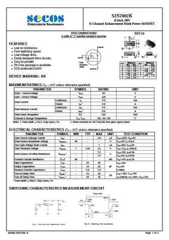
2N7002K N-CHANNEL ENHANCEMENT MODE MOSFET Features Mechanical Data Low On-Resistance Case SOT-23 Low Input Capacitance Case Material Molded Plastic, Green Molding Compound. UL Flammability Classification Rating 94V-0 Fast Switching Speed Moisture Sensitivity Level 1 per J-STD-020 Low Input/Output Leakage Terminals Finish Matte Tin an
2n7002k-tp.pdf
MCC TM Micro Commercial Components 20736 Marilla Street Chatsworth Micro Commercial Components 2N7002K CA 91311 Phone (818) 701-4933 Fax (818) 701-4939 Features Epoxy meets UL 94 V-0 flammability rating Moisture Sensitivity Level 1 High density cell design for low RDS(ON) Voltage controlled small signal switch N-Channel MOSFET Rugged and reliable Hig
2n7002ka.pdf
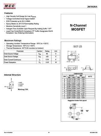
2N7002KA Features High Density Cell Design for Low RDS(ON) Voltage Controlled Small Signal Switch ESD Protected up to 2KV (HBM) Epoxy Meets UL 94 V-0 Flammability Rating N-Channel Moisture Sensitivity Level 1 Halogen Free Available Upon Request By Adding Suffix "-HF" MOSFET Lead Free Finish/RoHS Compliant ("P" Suffix Designates RoHS Compliant. See Ordering
2n7002kwa.pdf
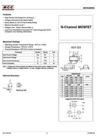
Features High Density Cell Design for Low RDS(ON) Voltage Controlled Small Signal Switch Epoxy Meets UL 94 V-0 Flammability Rating Moisture Sensitivity Level 1 Halogen Free. Green Device (Note 1) Lead Free Finish/RoHS Compliant ("P" Suffix Designates RoHS Compliant. See Ordering Information) Maximum Ratings Operating Junct
2n7002kw.pdf
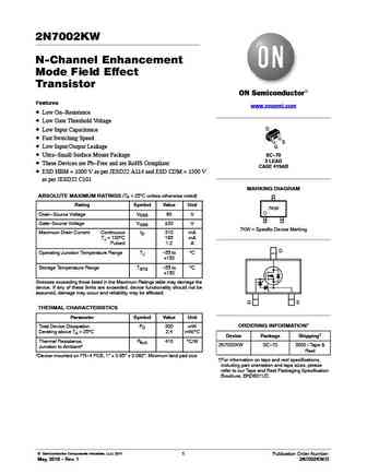
2N7002KW N-Channel Enhancement Mode Field Effect Transistor Features www.onsemi.com Low On-Resistance Low Gate Threshold Voltage D Low Input Capacitance Fast Switching Speed S Low Input/Output Leakage G Ultra-Small Surface Mount Package SC-70 3 LEAD These Devices are Pb-Free and are RoHS Compliant CASE 419AB ESD HBM = 1000 V as per JESD22 A114 a
2v7002k 2n7002k.pdf
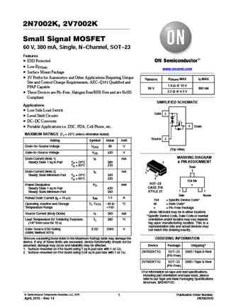
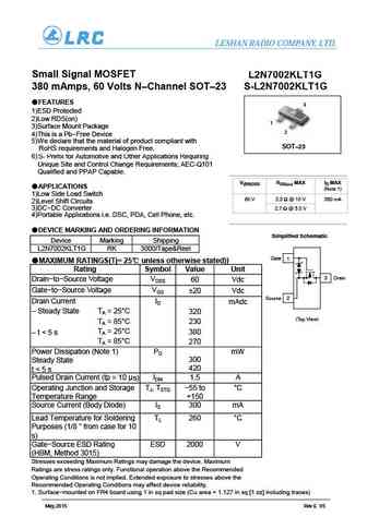
2N7002K, 2V7002K Small Signal MOSFET 60 V, 380 mA, Single, N-Channel, SOT-23 Features ESD Protected Low RDS(on) www.onsemi.com Surface Mount Package 2V Prefix for Automotive and Other Applications Requiring Unique V(BR)DSS RDS(on) MAX ID MAX Site and Control Change Requirements; AEC-Q101 Qualified and 1.6 W @ 10 V PPAP Capable 60 V 380 mA 2.5 W @ 4.5 V These D
2n7002k 2v7002k.pdf
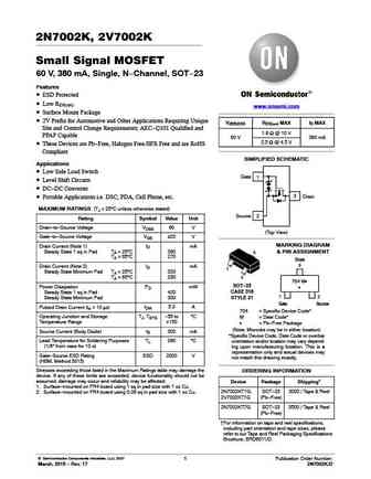
2N7002K, 2V7002K Small Signal MOSFET 60 V, 380 mA, Single, N-Channel, SOT-23 Features ESD Protected Low RDS(on) www.onsemi.com Surface Mount Package 2V Prefix for Automotive and Other Applications Requiring Unique V(BR)DSS RDS(on) MAX ID MAX Site and Control Change Requirements; AEC-Q101 Qualified and 1.6 W @ 10 V PPAP Capable 60 V 380 mA 2.5 W @ 4.5 V These D
2n7002kt1g.pdf
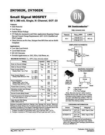
2N7002K, 2V7002K Small Signal MOSFET 60 V, 380 mA, Single, N-Channel, SOT-23 Features ESD Protected Low RDS(on) http //onsemi.com Surface Mount Package 2V Prefix for Automotive and Other Applications Requiring Unique V(BR)DSS RDS(on) MAX ID MAX Site and Control Change Requirements; AEC-Q101 Qualified and 1.6 W @ 10 V PPAP Capable 60 V 380 mA 2.5 W @ 4.5 V Thes
2n7002kl-ae2-r 2n7002kg-ae2-r.pdf
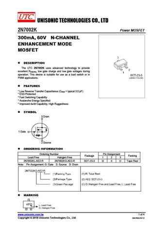
UNISONIC TECHNOLOGIES CO., LTD 2N7002K Power MOSFET 300mA, 60V N-CHANNEL ENHANCEMENT MODE MOSFET DESCRIPTION The UTC 2N7002K uses advanced technology to provide excellent RDS(ON), low gate charge and low gate voltages during operation. This device is suitable for use as a load switch or in PWM applications. FEATURES * Low Reverse Transfer Capacitance (CRSS = typica
2n7002k.pdf
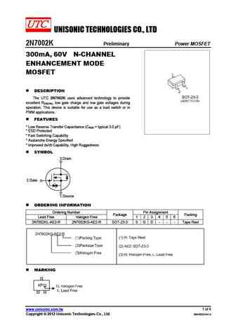
UNISONIC TECHNOLOGIES CO., LTD 2N7002K Preliminary Power MOSFET 300mA, 60V N-CHANNEL ENHANCEMENT MODE MOSFET DESCRIPTION The UTC 2N7002K uses advanced technology to provide excellent RDS(ON), low gate charge and low gate voltages during operation. This device is suitable for use as a load switch or in PWM applications. FEATURES * Low Reverse Transfer Capacitance (CRSS
2n7002k.pdf
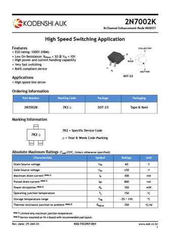
2N7002K N-Channel Enhancement Mode MOSFET High Speed Switching Application COLLECTOR Features 3 ESD rating 1000V (HBM) 3 Low On-Resistance R
2n7002ku.pdf
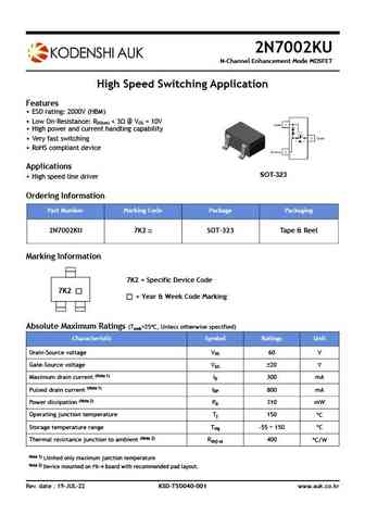
2N7002KU N-Channel Enhancement Mode MOSFET High Speed Switching Application Features ESD rating 2000V (HBM) Low On-Resistance R
2n7002ks6.pdf
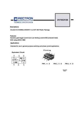
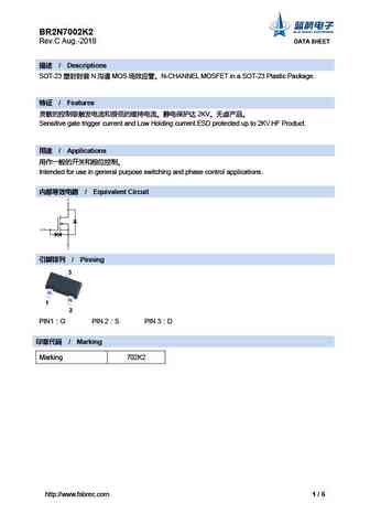
2N7002KS6 Descriptions N-CHANNEL MOSFET in a SOT-363 Plastic Package. Features Sensitive gate trigger current and Low Holding current.ESD protected diode. ESD rating 2200V HBM Applications Intended for use in general purpose switching and phase control applications. Pi nni ng Equivalent Circuit PIN1 4 S PIN 2 5 G PIN 3 6 D 2018-10/33 REV D Absolute Maximum Ratings(Ta=25
2n7002kw.pdf
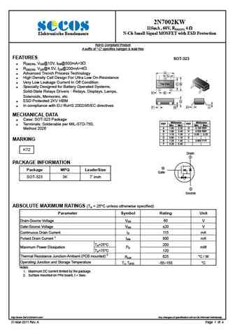
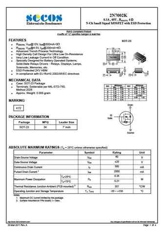
2N7002KW 115mA , 60V, RDS(ON) 4 N-Ch Small Signal MOSFET with ESD Protection Elektronische Bauelemente RoHS Compliant Product A suffix of -C specifies halogen & lead-free FEATURES SOT-323 RDS(ON), VGS@10V, IDS@500mA=3 RDS(ON), VGS@4.5V, IDS@200mA=4 A Advanced Trench Process Technology L High Density Cell Design For Ultra Low On-Resistance
2n7002k.pdf
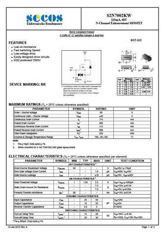
2N7002K 0.3A , 60V , RDS(ON) 4 N-Ch Small Signal MOSFET with ESD Protection Elektronische Bauelemente RoHS Compliant Product A suffix of -C specifies halogen & lead-free FEATURES SOT-23 RDS(ON), VGS@10V, IDS@500mA=3 RDS(ON), VGS@4.5V, IDS@200mA=4 A L Advanced Trench Process Technology 3 3 High Density Cell Design For Ultra Low On-Resista
s2n7002k.pdf
S2N7002K 115mA, 60V N-Channel Enhancement Mode Power MOSFET Elektronische Bauelemente RoHS Compliant Product SOT-23 A Suffix of -C specifies halogen & lead-free A L 3 3 Top View C B FEATURES 1 1 2 3 DRAIN 2 Low on resistance. K E Fast switching speed. D Low-voltage drive. 1 H J F G GATE * Easily designed drive circuits. Easy to parallel.
s2n7002kw.pdf
S2N7002KW 115mA, 60V N-Channel Enhancement MOSFET Elektronische Bauelemente RoHS Compliant Product A Suffix of -C specifies halogen & lead-free SOT-323 FEATURES Low on-resistance Fast switching Speed A L Low-voltage drive 3 3 Easily designed drive circuits Top View C B 1 1 2 ESD protected 1500V 2 K E D H J F G Millimeter Millimeter REF. REF.
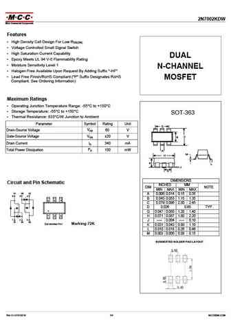
2n7002kdw.pdf
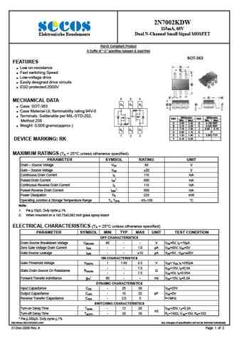
2N7002KDW 115mA, 60V Dual N-Channel Small Signal MOSFET Elektronische Bauelemente RoHS Compliant Product A Suffix of -C specifies halogen & lead-free SOT-363 FEATURES A Low on-resistance E L Fast switching Speed 6 5 4 Low-voltage drive Easily designed drive circuits B ESD protected 2000V 1 2 3 F C H 6 5 4 MECHANICAL DATA J D2 G1 S1 D
tsm2n7002kdcu6.pdf
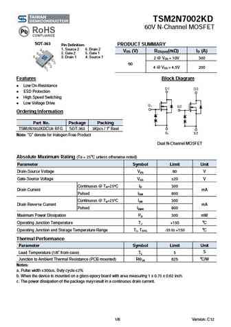
TSM2N7002KD 60V N-Channel MOSFET SOT-363 PRODUCT SUMMARY Pin Definition 1. Source 2 6. Drain 2 VDS (V) RDS(on)(m ) ID (A) 2. Gate 2 5. Gate 1 3. Drain 1 4. Source 1 2 @ VGS = 10V 300 60 4 @ VGS = 4.5V 200 Features Block Diagram Low On-Resistance ESD Protection High Speed Switching Low Voltage Drive Ordering Information Part No. Package Pa
tsm2n7002kcx.pdf
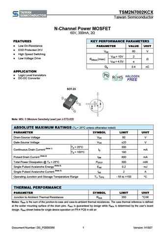
TSM2N7002KCX Taiwan Semiconductor N-Channel Power MOSFET 60V, 300mA, 2 FEATURES KEY PERFORMANCE PARAMETERS Low On-Resistance PARAMETER VALUE UNIT ESD Protected 2KV VDS 60 V High Speed Switching VGS = 10V 2 Low Voltage Drive RDS(on) (max) VGS = 4.5V 4 Qg 0.4 nC APPLICATION Logic Level translators DC-DC Converter SOT-23 Note
tsm2n7002kcu tsm2n7002kcx.pdf
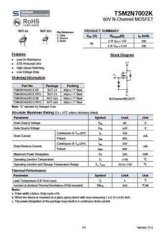
TSM2N7002K 60V N-Channel MOSFET SOT-23 SOT-323 PRODUCT SUMMARY Pin Definition 1. Gate VDS (V) RDS(on)( ) ID (mA) 2. Source 3. Drain 2 @ VGS = 10V 300 60 4 @ VGS = 4.5V 200 Features Block Diagram Low On-Resistance ESD Protected 2KV High Speed Switching Low Voltage Drive Ordering Information Part No. Package Packing TSM2N7002KCX RF SOT-23
2n7002kw.pdf
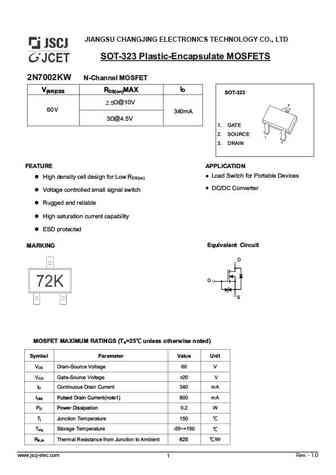
JIANGSU CHANGJING ELECTRONICS TECHNOLOGY CO., LTD SOT-323 Plastic-Encapsulate MOSFETS 2N7002KW N-Channel MOSFET ID V(BR)DSS RDS(on)MAX SOT-323 2.5 3 1. GATE 2. SOURCE 1 2 3. DRAIN FEATURE APPLICATION High density cell design for Low RDS(on) Voltage controlled sm
2n7002k.pdf
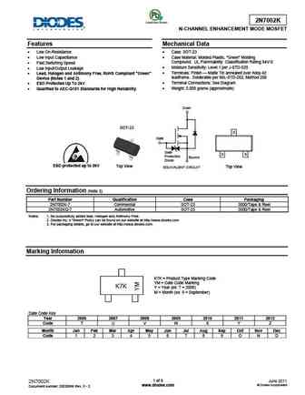
JIANGSU CHANGJIANG ELECTRONICS TECHNOLOGY CO., LTD SOT-23 Plastic-Encapsulate MOSFETs 2N7002K N-channel MOSFET SOT-23 FEATURES z High density cell design for Low RDS on z Voltage controlled small signal switch 1. GATE 2. SOURCE z Rugged and reliable 3. DRAIN z High saturation current capability z ESD protected up to 2KV Marking 72K Equivalent circuit MOSFET
2n7002kdw.pdf
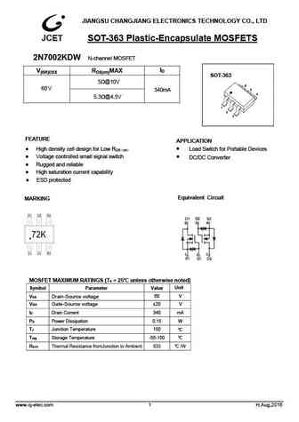
JIANGSU CHANGJIANG ELECTRONICS TECHNOLOGY CO., LTD SOT-363 Plastic-Encapsulate MOSFETS 2N7002KDW N-channel MOSFET ID V(BR)DSS RDS(on)MAX SOT-363 5 @10V 6 60V 5 340mA 4 5.3 @4.5V 1 2 3 FEATURE APPLICATION z High density cell design for Low RDS on Load Switch for Portable Devices z Voltage controlled small signal switch DC/DC Converter z Rugged
2n7002k.pdf
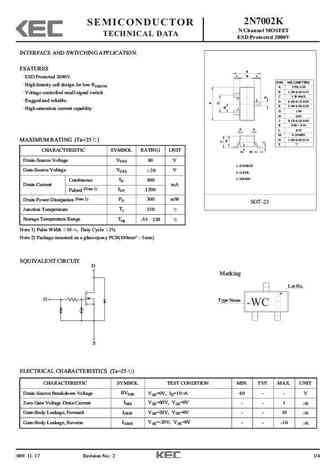
2N7002K SEMICONDUCTOR N Channel MOSFET TECHNICAL DATA ESD Protected 2000V INTERFACE AND SWITCHING APPLICATION. FEATURES E L B L ESD Protected 2000V. DIM MILLIMETERS High density cell design for low RDS(ON). _ A + 2.93 0.20 B 1.30+0.20/-0.15 Voltage controlled small signal switch. C 1.30 MAX 2 3 Rugged and reliable. D 0.45+0.15/-0.05 E 2.40+0.30/-0.20 High saturation curr
2n7002ka.pdf
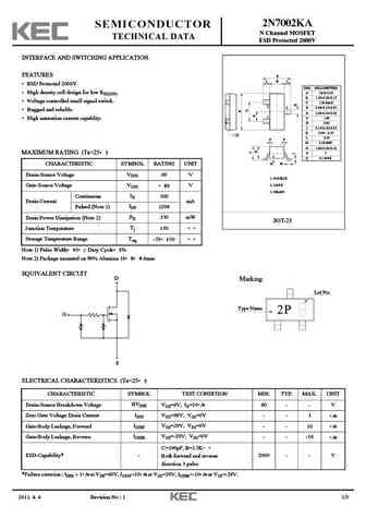
2N7002KA SEMICONDUCTOR N Channel MOSFET TECHNICAL DATA ESD Protected 2000V INTERFACE AND SWITCHING APPLICATION. FEATURES E L B L ESD Protected 2000V. DIM MILLIMETERS _ + High density cell design for low RDS(ON). A 2.93 0.20 B 1.30+0.20/-0.15 Voltage controlled small signal switch. C 1.30 MAX 2 3 D 0.40+0.15/-0.05 Rugged and reliable. E 2.40+0.30/-0.20 1 G 1.90
2n7002k.pdf
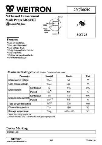
2N7002K N-Channel Enhancement 3 DRAIN Mode Power MOSFET 3 1 P b Lead(Pb)-Free 1 GATE * 2 * Gate Pretection Diode SOURCE 2 SOT-23 Features * Low on-resistance. * Fast switching speed. * Low-voltage drive. * Easily designed drive circuits. * Easy to parallel. * Pb-Free package is available. * Esd Protected 2000V Maximum Ratings(T = 25 Unless Otherwise Specified) A
2n7002kdw.pdf
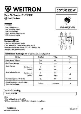
2N7002KDW Dual N-Channel MOSFET 6 5 P b Lead(Pb)-Free 4 1 2 3 Features * Low On-Resistance SOT-363(SC-88) * Fast Switching Speed * Low-voltage drive 6 5 4 * Easily designed drive circuits D2 G1 S1 * ESD Protected 2000V Mechanical Data *Case SOT-363, Molded Plastic *Case Material-UL Flammability Rating 94V-0 S2 G2 D1 *Terminals Solderable per MIL-STD-202, Method 208 1 2
2n7002kt.pdf
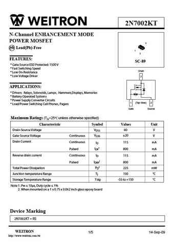
2N7002KT N-Channel ENHANCEMENT MODE POWER MOSFET 3 P b Lead(Pb)-Free 1 2 FEATURES SC-89 * Gate-Source ESD Protected 1500 V * Fast Switching Speed Drain * Low On-Resistance * Low Voltage Driver 3 APPLICATIONS * Drivers Relays, Solenoids, Lamps, Hammers,Displays, Memories * Battery Operated Systems * Power Supply Converter Circuits 1 (Top View) 2 * Load/Power Switching Ce
h2n7002ksn.pdf
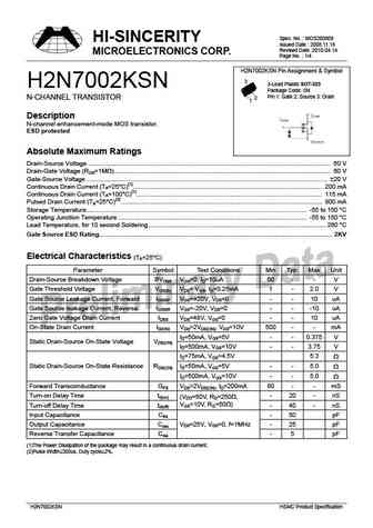
Spec. No. MOS200809 HI-SINCERITY Issued Date 2008.11.18 Revised Date 2010.04.14 MICROELECTRONICS CORP. Page No. 1/4 H2N7002KSN Pin Assignment & Symbol 3 3-Lead Plastic SOT-323 H2N7002KSN Package Code SN Pin 1 Gate 2 Source 3 Drain N-CHANNEL TRANSISTOR 2 1 Description N-channel enhancement-mode MOS transistor. ESD protected Absolute Maximum Ratings Drai
h2n7002k.pdf
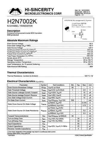
Spec. No. MOS200803 HI-SINCERITY Issued Date 2005.03.13 Revised Date 2010,03,04 MICROELECTRONICS CORP. Page No. 1/5 H2N7002K N-CHANNEL TRANSISTOR Description N-channel enhancement-mode MOS transistor. ESD protected Absolute Maximum Ratings Drain-Source Voltage .........................................................................................................
ap2n7002k-hf.pdf
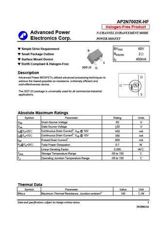
AP2N7002K-HF Halogen-Free Product Advanced Power N-CHANNEL ENHANCEMENT MODE Electronics Corp. POWER MOSFET Simple Drive Requirement BVDSS 60V D Small Package Outline RDS(ON) 2 Surface Mount Device ID 450mA S RoHS Compliant & Halogen-Free SOT-23 G Description D Advanced Power MOSFETs utilized advanced processing techniques to achieve the lowest possible on-resist
ap2n7002ku.pdf
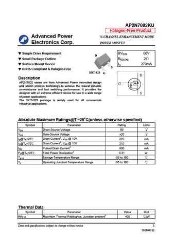
AP2N7002KU Halogen-Free Product Advanced Power N-CHANNEL ENHANCEMENT MODE Electronics Corp. POWER MOSFET Simple Drive Requirement BVDSS 60V D Small Package Outline RDS(ON) 2 Surface Mount Device ID 270mA S RoHS Compliant & Halogen-Free SOT-323 G D Description AP2N7002 series are from Advanced Power innovated design G and silicon process technology to achieve th
2n7002k.pdf
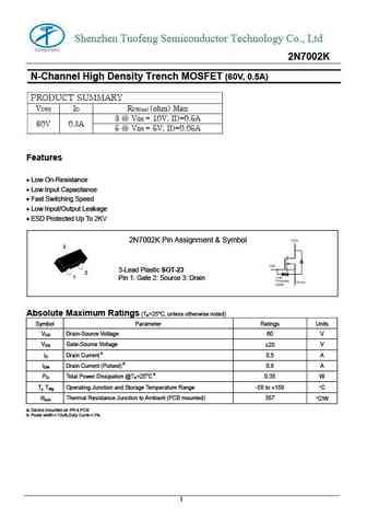
Shenzhen Tuofeng Semiconductor Technology Co., Ltd 2N7002K N-Channel High Density Trench MOSFET (60V, 0.5A) PRODUCT SUMMARY VDSS ID RDS(on) (ohm) Max 3 @ VGS = 10V, ID=0.5A 60V 0.5A 5 @ VGS = 5V, ID=0.05A Features Low On-Resistance Low Input Capacitance Fast Switching Speed Low Input/Output Leakage ESD Protected Up To 2KV 2N7002K Pin Assignment & Symbol
2n7002kg8.pdf
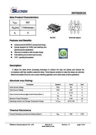
2N7002KG8 Main Product Characteristics VDSS 60V RDS(on) 7.5ohm(max.) ID A SOT-363 Sc he mat i c d ia gra m Features and Benefits Advanced trench MOSFET process technology Special designed for PWM, load switching and general purpose applications Ultra low on-resistance with low gate charge Fast switching and reverse body recovery 150 operating t
2n7002k.pdf
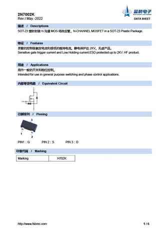
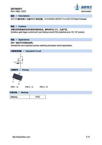
2N7002K Rev.I May.-2022 DATA SHEET / Descriptions SOT-23 N MOS N-CHANNEL MOSFET in a SOT-23 Plastic Package. / Features 2KV Sensitive gate trigger current and Low Holding current.ESD protected up to 2KV. HF product. / Applications
l2n7002klt1g.pdf
LESHAN RADIO COMPANY, LTD. Small Signal MOSFET L2N7002KLT1G 380 mAmps, 60 Volts N Channel SOT 23 S-L2N7002KLT1G FEATURES 3 1)ESD Protected 2)Low RDS(on) 1 3)Surface Mount Package 2 4)This is a Pb-Free Device 5)We declare that the material of product compliant with SOT 23 RoHS requirements and Halogen Free. 6) S- Prefix for Automotive and Other Applications Requiring Un
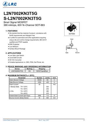
l2n7002kdw1t1g l2n7002kdw1t3g.pdf
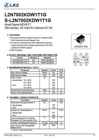
L2N7002KDW1T1G S-L2N7002KDW1T1G Small Signal MOSFET 380 mAmps, 60 Volts N Channel SC-88 1. FEATURES We declare that the material of product compliance with RoHS requirements and Halogen Free. S- prefix for automotive and other applications requiring unique site and control change requirements; AEC-Q101 SC88(SOT-363) qualified and PPAP capable. ESD Protected 2. D
2n7002k.pdf
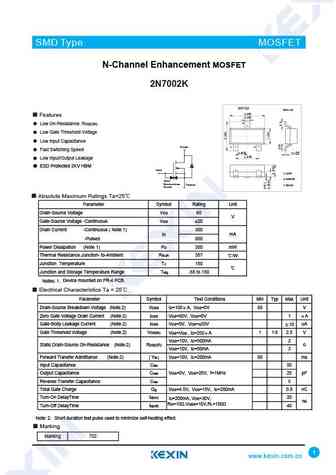
SMD Type MOSFET N-Channel Enhancement MOSFET 2N7002K SOT-23 Unit mm +0.1 2.9 -0.1 Features +0.1 0.4 -0.1 3 Low On-Resistance RDS(ON) Low Gate Threshold Voltage Low Input Capacitance D rai n 1 2 Fast Switching Speed +0.1 +0.05 0.95 -0.1 0.1 -0.01 +0.1 1.9 -0.1 Low Input/Output Leakage ESD Protected 2KV HBM Gate 1.Base 1 GATE 2.Emitter 2 SOURCE Gate Protectio
2n7002k-3.pdf
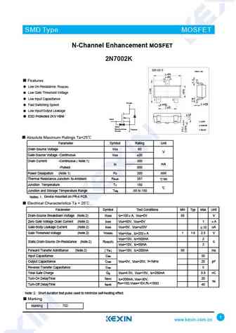
SMD Type MOSFET N-Channel Enhancement MOSFET 2N7002K SOT-23-3 Unit mm +0.2 2.9-0.1 +0.1 0.4 -0.1 Features 3 Low On-Resistance RDS(ON) Low Gate Threshold Voltage Low Input Capacitance 1 2 D rai n +0.02 +0.1 0.15 -0.02 0.95 -0.1 Fast Switching Speed +0.1 1.9-0.2 Low Input/Output Leakage ESD Protected 2KV HBM Gate 1.Base 1 GATE 2.Emitter 2 SOURCE Gate Protect
2n7002kw.pdf
2N7002KW 60V N-Channel Enhancement Mode MOSFET - ESD Protected FEATURES RDS(ON), VGS@10V,IDS@500mA=3 RDS(ON), VGS@4.5V,IDS@200mA=4 Advanced Trench Process Technology High Density Cell Design For Ultra Low On-Resistance Very Low Leakage Current In Off Condition Specially Designed for Battery Operated Systems, Solid-State Relays Drivers Relays, Displays, La
2n7002k.pdf
2N7002K 60V N-Channel Enhancement Mode MOSFET - ESD Protected FEATURES RDS(ON), VGS@10V,IDS@500mA=3 RDS(ON), VGS@4.5V,IDS@200mA=4 0.120(3.04) 0.110(2.80) Advanced Trench Process Technology High Density Cell Design For Ultra Low On-Resistance Very Low Leakage Current In Off Condition 0.056(1.40) Specially Designed for Battery Operated Systems, Solid-State R
2n7002kdw.pdf
2N7002KDW 60V N-Channel Enhancement Mode MOSFET - ESD Protected FEATURES RDS(ON), VGS@10V,IDS@500mA=3 RDS(ON), VGS@4.5V,IDS@200mA=4 Advanced Trench Process Technology High Density Cell Design For Ultra Low On-Resistance Very Low Leakage Current In Off Condition Specially Designed for Battery Operated Systems, Solid-State Relays Drivers Relays, Displays, L
2n7002ktb.pdf
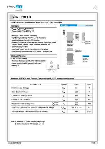
2N7002KTB 60V N-Channel Enhancement Mode MOSFET - ESD Protected FEATURES RDS(ON), VGS@10V,IDS@500mA=3 RDS(ON), VGS@4.5V,IDS@200mA=4 Advanced Trench Process Technology High Density Cell Design For Ultra Low On-Resistance Very Low Leakage Current In Off Condition 0.052(1.30) 0.024(0.60) Specially Designed for Battery Operated Systems, Solid-State Relays 0.
am2n7002k.pdf
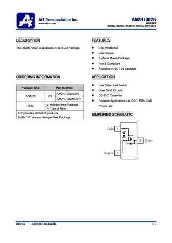
AiT Semiconductor Inc. AM2N7002K www.ait-ic.com MOSFET SMALL SIGNAL MOSFET 380mA, 60 VOLTS DESCRIPTION FEATURES The AM2N7002K is available in SOT-23 Package ESD Protected Low R DS(ON) Surface Mount Package RoHS Compliant Available in SOT-23 package ORDERING INFORMATION APPLICATION Low Side Load Switch Package Type Part Number Level Shift Circ
cmt2n7002k.pdf
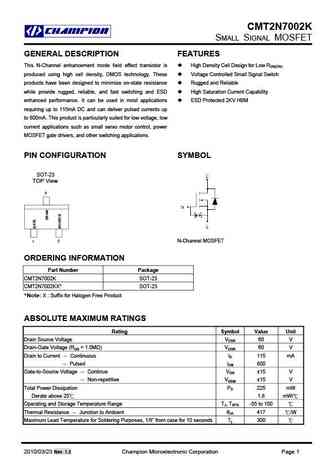
CMT2N7002K SMALL SIGNAL MOSFET GENERAL DESCRIPTION FEATURES This N-Channel enhancement mode field effect transistor is High Density Cell Design for Low RDS(ON) produced using high cell density, DMOS technology. These Voltage Controlled Small Signal Switch products have been designed to minimize on-state resistance Rugged and Reliable while provide rugged, reliable, and fast sw
2n7002k.pdf
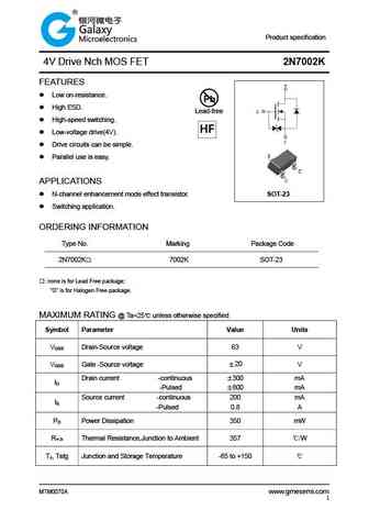
Product specification 4V Drive Nch MOS FET 2N7002K FEATURES Low on-resistance. Pb High ESD. Lead-free High-speed switching. Low-voltage drive(4V). Drive circuits can be simple. Parallel use is easy. APPLICATIONS N-channel enhancement mode effect transistor. SOT-23 Switching application. ORDERING INFORMATION Type No. Marking Packag
k2n7002k.pdf
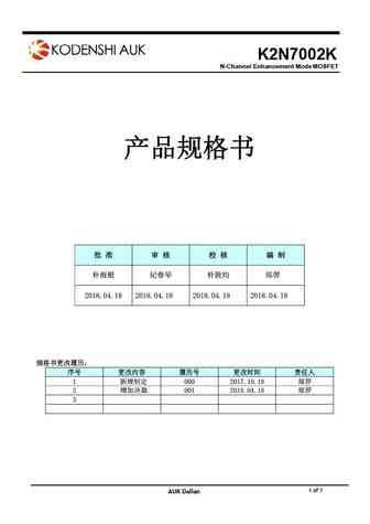
K2N7002K N-Channel Enhancement Mode MOSFET 2018.04.18 2018.04.18 2018.04.18 2018.04.18 1 000 2017.10.18 2 001 2018.04.18 3 1 of 7 AUK Dalian K2N7002K N-Channel Enh
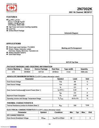
2n7002k.pdf
Pb Free Product http //www.ncepower.com 2N7002K NCE N-Channel Enhancement Mode Power MOSFET General Features VDS = 60V,ID = 0.3A RDS(ON)
a2n7002k.pdf
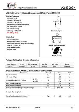
http //www.ncepower.com A2N7002K NCE Automotive N-Channel Enhancement Mode Power MOSFET General Features V = 60V,I = 0.3A DS D R
2n7002kw.pdf
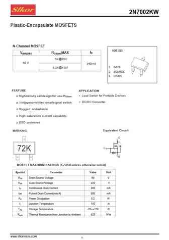
2N7002KW Plastic-Encapsulate MOSFETS N-Channel MOSFET SOT-323 I V(BR)DSS RDS(on)MAX D 3 5K@10V 60 V 340mA 1. GATE 5.3K@4.5V 2. SOURCE 1 2 3. DRAIN FEATURE APPLICATION Load Switch for Portable Devices z Highdensity celldesign for Low R DS(on) DC/DC Converter z Voltagecontrolled smallsignal switch z Rugged andreliable z High saturation current capability z ESD pro
2n7002k.pdf
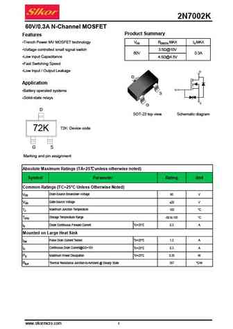
2N7002K 60V/0.3A N-Channel MOSFET Product Summary Features Trench Power MV MOSFET technology VDS RDS(ON) MAX ID MAX Voltage controlled small signal switch 3.5 @10VD2 60V S1 0.3A D1 Low input Capacitance 4.5 @4.5V Fast Switching Speed Low Input / Output Leakage D Application Battery operated systems S Solid-state relays G D SOT-23 top view Schematic dia
2n7002kdw.pdf
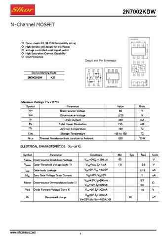
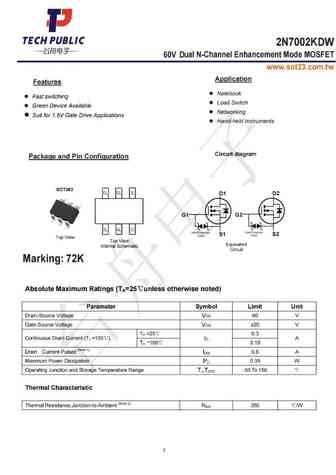
2N7002KDW N- Channel MOSFET Epoxy meets UL 94 V-0 flammability rating High density cell design for low RDS(ON) Voltage controlled small signal switch High Saturation Current Capability ESD Protected Device Marking Code 2N7002KDW K27 Maximum Ratings Ta = 25 Symbol Parameter Value Units VDS Drain-source Voltage 60 V VGS Gate-source-Voltage 20 V
2n7002kt.pdf
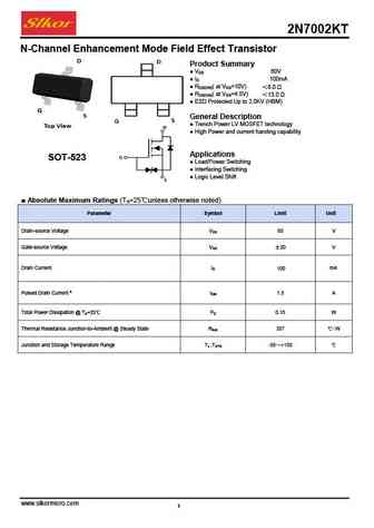
2N7002KT N-Channel Enhancement Mode Field Effect Transistor Product Summary V 60V DS I 100mA D R ( at V =10V) 8.0 DS(ON) GS R ( at V =4.5V) 13.0 DS(ON) GS ESD Protected Up to 2.0KV (HBM) General Description Trench Power LV MOSFET technology High Power and current handing capability Applications SOT-523 Load/Power Switching Int
2n7002kw.pdf
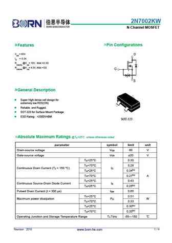
2N7002KW N-Channel MOSFET Pin Configurations Features V = 60V DS I D = 0.3A R @V = 10V, Max =2.3 DS(ON) GS R @V = 4.5V, Max =3 DS(ON) GS General Description Super High dense cell design for extremely low RDS(ON) Reliable and Rugged. SOT-323 for Surface Mount Package. ESD Rating >2000VHBM SOT-323 Absolute Maximum Ratings @T =25 unless othe
2n7002k.pdf
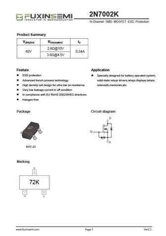
2N7002K N-Channel SMD MOSFET ESD Protection Product Summary V(BR)DSS RDS(on)MAX ID 2.8 @10V 60V 0.34A 3.6 @4.5V Feature Application ESD protection Specially designed for battery operated system, Advanced trench process technology solid-state relays drivers,relays,displays,lamps, High density cell design for ultra low on-resistance solenoids,memories,etc. Very low leaka
2n7002kd.pdf
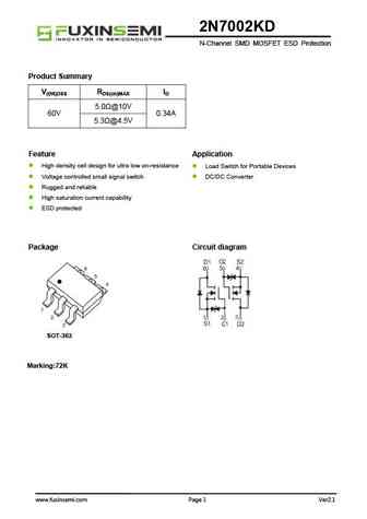
2N7002KD N-Channel SMD MOSFET ESD Protection Product Summary V(BR)DSS RDS(on)MAX ID 5.0 @10V 60V 0.34A 5.3 @4.5V Feature Application High density cell design for ultra low on-resistance Load Switch for Portable Devices Voltage controlled small signal switch DC/DC Converter Rugged and reliable High saturation current capability ESD protected Package Circuit diagram
et2n7002k.pdf
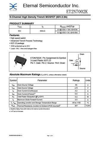
Eternal Semiconductor Inc. ET2N7002K N-Channel High Density Trench MOSFET (60V,0.5A) PRODUCT SUMMARY VDSS ID RDS(on) (m )Typ 2.5 @ VGS = 10V, ID=0.5A 60V 500mA 3.0 @ VGS = 5V, ID=0.05A Features High speed switch Advanced Trench Process Technology SOT-23 package ESD protected up to 2KV Lead Pb -free and halogen-free Drain ET2N7002K Pin Assignment & Symbo
2n7002k.pdf
Plastic-Encapsulate Diodes FEATURE 2N7002K High density cell design for low RDS(ON) N-Channel MOSFET Voltage controlled small signal switch Rugged and reliable High saturation current capability ESD Protected Up To 2k V MAXIMUM RATINGS (Ta=25 unless otherwise noted) Parameter Symbol Value Unit 1.Gate Drain-Source Voltage VDS 60 V 2.Source SOT-23 3.Drain Gate-Sou
hss2n7002k.pdf
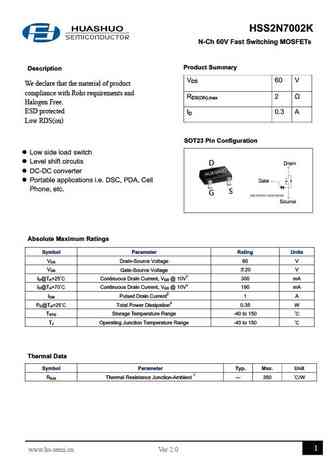
HSS2N7002K N-Ch 60V Fast Switching MOSFETs Product Summary Description VDS 60 V We declare that the material of product compliance with Rohs requirements and RDS(ON),max 2 Halogen Free. ESD protected ID 0.3 A Low RDS(on) SOT23 Pin Configuration l Low side load switch l Level shift circutis l DC-DC converter l Portable applications i.e. DSC, PDA, Cell Phone,
2n7002k.pdf
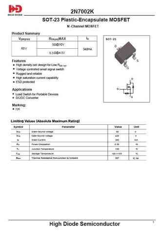
2N7002K SOT-23 Plastic-Encapsulate MOSFET N -Channel MOSFET roduct Summary P ID V(BR)DSS RDS(on)MAX SOT- 23 5 @10V D 60V mA 340 @4.5V 5.3 S Features High density cell design for Low RDS on G Voltage controlled small signal switch Rugged and reliable High saturation current capability ESD protected Applications Load
jmtd2n7002ks.pdf
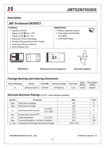
JMTD2N7002KS Description JMT N-channel MOSFET Features Application V =60V, I =0.2A Battery Operated Systems DS D R
jmtla2n7002ks.pdf
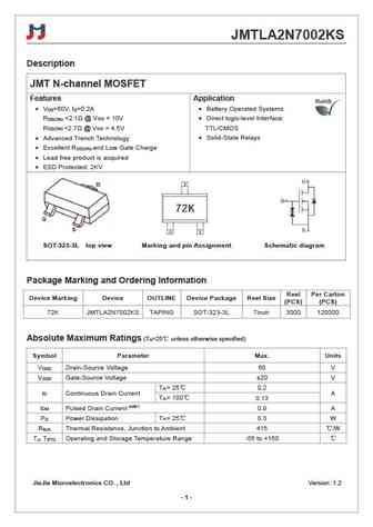
JMTLA2N7002KS Description JMT N-channel MOSFET Features Application V =60V, I =0.2A Battery Operated Systems DS D R
jmtl2n7002ks.pdf
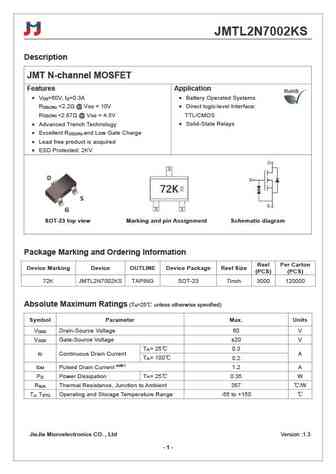
JMTL2N7002KS Description JMT N-channel MOSFET Features Application V =60V, I =0.3A Battery Operated Systems DS D R
jmtlb2n7002kds.pdf
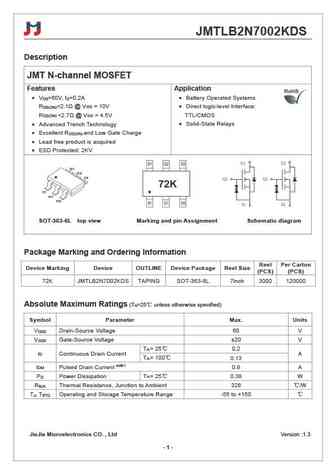
JMTLB2N7002KDS Description JMT N-channel MOSFET Features Application V =60V, I =0.2A Battery Operated Systems DS D R
2n7002kt.pdf
2N7002KT SOT-523 Plastic-Encapsulate Mosfets Features Gate 1 High density cell design for low R DS (ON) Voltage controlled small signal switch 3 Drain Rugged and reliable High saturation current capability Source 2 Applications (Top View) Load Switch for Portable Devices DC/DC Converter Marking KN Maximum Ratings (T =25 C unless otherwise spe
2n7002k.pdf
2N7002K 60V,0.34A N-Channel Mosfet SOT-23 FEATURES RDS(ON) 2.3 @VGS=10V RDS(ON) 2.7 @VGS=4.5V APPLICATIONS Portable appliances MARKING N-CHANNEL MOSFET 7002 Device Code Maximum ratings (Ta=25 unless otherwise noted) Parameter Symbol Value Unit Drain-Source Voltage VDS 60 V Gate-Source Voltage VGS 20 I 0.34 D* Continuous Drain Current* Pulsed Drain Current*
2n7002k.pdf
2N7002K SOT-23 Plastic-Encapsulate MOSFETS 60V N-Channel Enhancement Mode MOSFET V(BR)DSS RDS(on)Typ ID MAX SO T -23 3 0.9 @10V 60V mA 500 @4.5V 1.1 1. GATE 2. SOURCE 1 2 3. DRAIN FEATURE APPLICATION Load Switch for Portable Devices High density cell design for low RDS(ON) DC/DC Converter Voltage controlled small signal switch Rugged and reliable
2n7002kw.pdf
DATA SHEET 2N7002KW N-CHANNELENHANCEMENT MODE FIELD EFFECT TRANSISTOR VOLTAGE 60 Volts CURRENT 300 mA FEATURES N-CHANNEL ENHANCEMENT MODE FIELD EFFECT TRANSISTOR, DESIGNED FOR HIGH SPEED PULSE AMPLIFIER AND DRIVE APPLICATION. ESD MIL-STD883 , 1KV CONTACT DISCHARGE COMPLIANT PROTECTION. LEAD FREE AND HALOGEN-FREE. MECHANICAL DATA HIGDENSITY CELL DESIGN FOR LOW RDS
2n7002k.pdf
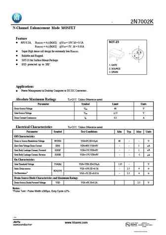
2N7002K N-Channel Enhancement Mode MOSFET Feature SOT-23 60V/0.2A, RDS(ON) = 4 (MAX) @VGS = 10V. Id = 0.5A RDS(ON) = 4 (MAX) @VGS = 5V . Id = 0.05A Super High dense cell design for extremely low RDS(ON) . Reliable and Rugged. SOT-23 for Surface Mount Package. ESD protected up to 2K V 1. GATE 2. SOURCE 3. DRAIN Applications Power Management in Desktop Comp
agm2n7002k3.pdf
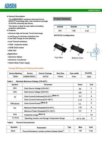
AGM2N7002K3 Typical Performance Characteristics www.agm-mos.com 3 VER2.65 AGM2N7002K3 SOT23 Marking Instructions www.agm-mos.com 5 VER2.65 AGM2N7002K3 Disclaimer The information provided in this document is believed to be accurate and reliable. However,Shenzhen Core Control Source Electronics Technology Co., Ltd. does not assume any responsibility for the following consequence
2n7002k.pdf
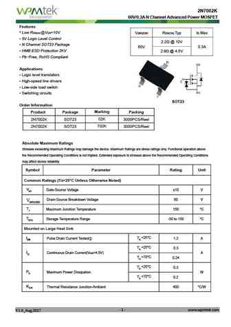
2N7002K 60V/0.3A N Channel Advanced Power MOSFET Features Low RDS(on) @VGS=10V V R Typ I Max (BR)DSS DS(ON) D 5V Logic Level Control 2.2 @ 10V N Channel SOT23 Package 60V 0.3A HMB ESD Protection 2KV 2.8 @ 4.5V Pb-Free, RoHS Compliant Applications Logic level translators High-speed line drivers Low-side load switch Switching circu
2n7002kh.pdf
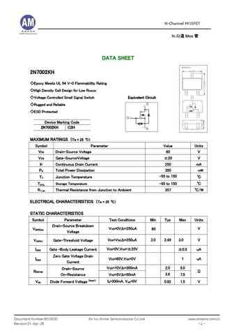
N-Channel MOSFET N- Mos DATA SHEET 2N7002KH Epoxy Meets UL 94 V-0 Flammability Rating High Density Cell Design for Low RDS(ON) Voltage Controlled Small Signal Switch Equivalent Circuit Rugged and Reliable ESD Protected Device Marking Code 2N7002KH C2H MAXIMUM RATINGS Ta = 25 Symbol Parameter Value Units VDS Drain-Source Voltage 60 V VGS Gate-Sour
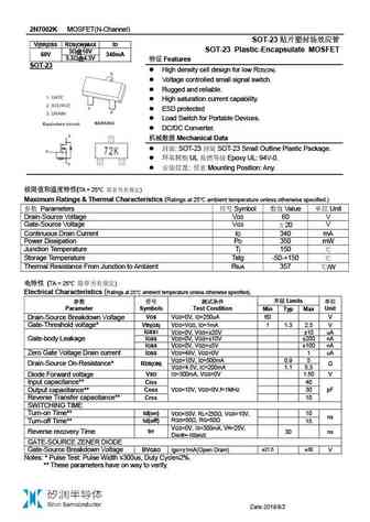
2n7002km.pdf
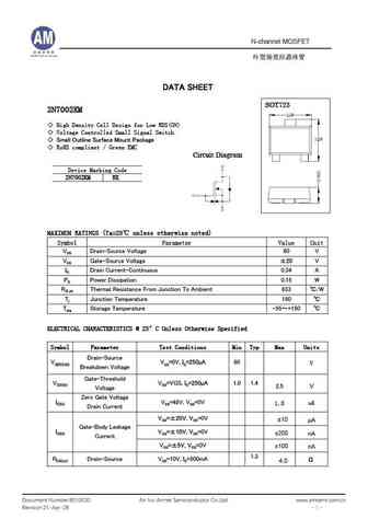
N-channel MOSFET N DATA SHEET SOT723 2N7002KM High Density Cell Design for Low RDS(ON) Voltage Controlled Small Signal Switch Small Outline Surface Mount Package RoHS compliant / Green EMC Circuit Diagram Device Marking Code 2N7002KM RK MAXIMUM RATINGS (Ta=25 unless otherwise noted) Symbol Parameter Value Unit VDS Drain-Sou
2n7002k.pdf
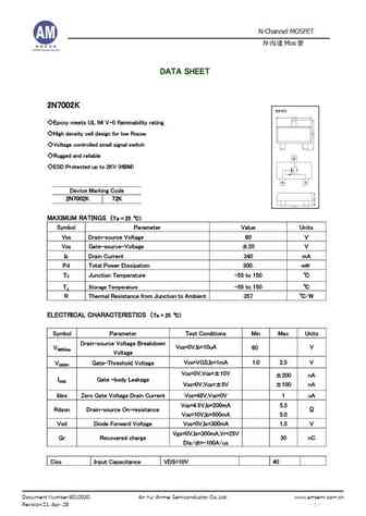
N-Channel MOSFET N- Mos DATA SHEET 2N7002K Epoxy meets UL 94 V-0 flammability rating High density cell design for low RDS(ON) Voltage controlled small signal switch Rugged and reliable ESD Protected up to 2KV (HBM) Device Marking Code 2N7002K 72K MAXIMUM RATINGS Ta = 25 Symbol Parameter Value Units VDS Drain-source Voltage 60 V VGS
2n7002kdw.pdf
2N7002KDW 60V N-Channel Enhancement Mode MOSFET - ESD Protected SOT-363 Unit inch (mm) FEATURES RDS(ON), VGS@10V,IDS@500mA=3 0.054(1.35) 0.045(1.15) RDS(ON), VGS@4.5V,IDS@200mA=4 Advanced Trench Process Technology High Density Cell Design For Ultra Low On-Resistance Very Low Leakage Current In Off Condition Specially Designed for Battery Operated Systems,
2n7002kw.pdf
2N7002KW SOT-323 N-Channel Enhancement MOSFET 3 Features Low On-Resistance RDS(ON) Low Gate Threshold Voltage 2 1.Gate Low Input Capacitance 2.Source Fast Switching Speed 3.Drain 1 Low Input/Output Leakage Simplified outline(SOT-323) ESD Protected 2KV HBM Drai n Gate Gate Protection Source Diode Absolute Maximum Ratings Ta=25 Parameter Symbol Rating Unit Drain
2n7002k.pdf
2N7002K MOSFET(N-Channel) SOT-23 V(BR)DSS RDS(ON)MAX ID SOT-23 Plastic-Encapsulate MOSFET 5 @10V 60V 340mA 5.3 @4.5V Features SOT-23 High density cell design for low RDS(ON). Voltage controlled small signal switch. Rugged and reliable. High saturation current capability. ESD protected Load Switch for Portable
2n7002k.pdf

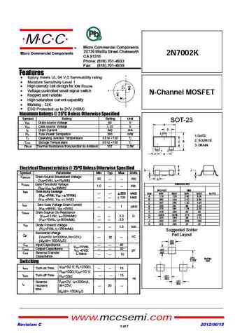
SHENZHEN LONG JING MICRO-ELECTRONICS CO., LTD. SOT-23 Plastic-Encapsulate Mosfets 2N7002K N-Channel Mosfet Features High density cell design for low R DS (ON) Voltage controlled small signal switch Rugged and reliable High saturation current capability ESD protected up to 2KV 1. Gate Marking 702 2. Source 3. Drain Maximum Ratings (T =25 C unless otherwise
wst2n7002k.pdf
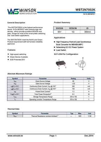
WST2N7002K N-Ch MOSFET Product Summery General Description The WST2N7002K is the highest performance BVDSS RDSON ID trench N-Ch MOSFET with extreme high cell density , which provide excellent RDSON and 60V 1 300mA gate charge for most of the small power switching and load switch applications. Applications The WST2N7002K meet the RoHS and Green Product requirement with
se2n7002k.pdf
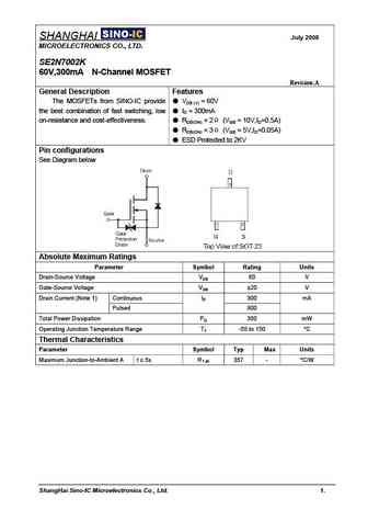
SHANGHAI July 2008 MICROELECTRONICS CO., LTD. SE2N7002K 60V,300mA N-Channel MOSFET Revision A General Description Features The MOSFETs from SINO-IC provide VDS (V) = 60V the best combination of fast switching, low ID = 300mA on-resistance and cost-effectiveness. RDS(ON)
vs2n7002k.pdf
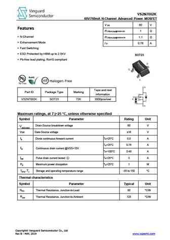
VS2N7002K 60V/760mA N-Channel Advanced Power MOSFET V DS 60 V Features R DS(on),typ@VGS=10V 1 N-Channel R DS(on),typ@VGS=4.5V 1.1 Enhancement Mode I D 0.76 A Fast Switching ESD Protected by HBM up to 2.5KV SOT23 Pb-free lead plating; RoHS compliant Tape and reel Part ID Package Type Marking information VS2N7002K SOT23 72K 3000pcs/reel
2n7002k.pdf
RoHS COMPLIANT 2N7002K N-Channel Enhancement Mode Field Effect Transistor Product Summary V 60V DS I 340mA D R ( at V =10V) 2.5ohm DS(ON) GS R ( at V =4.5V) 3.0ohm DS(ON) GS ESD Protected Up to 2.5KV (HBM) General Description Trench Power MV MOSFET technology Voltage controlled small signal switch Low input Capacitance F
2n7002kdw.pdf
RoHS COMPLIANT 2N7002KDW N-Channel Enhancement Mode Field Effect Transistor Product Summary V 60V DS I 340mA D R ( at V =10V) 2.5ohm DS(ON) GS R ( at V =4.5V) 3.0ohm DS(ON) GS ESD Protected Up to 2.5KV (HBM) General Description Trench Power MV MOSFET technology Voltage controlled small signal switch Low input Capacitance
ttx2n7002ka.pdf
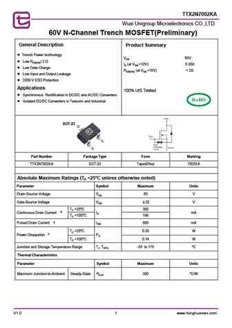
TTX2N7002KA Wuxi Unigroup Microelectronics CO.,LTD. 60V N-Channel Trench MOSFET(Preliminary) General Description Product Summary Trench Power technology VDS 60V Low RDS(ON) 2 ID (at VGS =10V) 0.35A Low Gate Charge RDS(ON) (at VGS =10V)
Otros transistores... 2SJ577, 2SJ578, 2SJ579, 2SJ580, 2SJ583LS, 2SJ584LS, 2SJ585LS, 2SJ589LS, IRF530, 2N7002KG8, SSF0115, SSF1006, SSF1006A, SSF1006H, SSF1007, SSF1009, SSF1010
🌐 : EN ES РУ

Liste
Recientemente añadidas las descripciónes de los transistores:
MOSFET: MSH100N045SA | MSD60P16 | MSD40P45 | MSB100N023 | MS60P03 | MS40P05AU | MS40P05 | MS40N05 | MS34P07 | MS34P01 | MS23P03 | MS23N06A | BPMS04N003M | BPM0405CG | BPM0306CG | BP0405SCG
Popular searches
2sc1913 | c2314 transistor | c2482 transistor | 2sc1222 replacement | 2sa725 | c5242 transistor | 2sa726 replacement | a1941 datasheet