SSF1020A MOSFET Equivalente. Reemplazo. Hoja de especificaciones. Principales características
Número de Parte: SSF1020A
Tipo de FET: MOSFET
Polaridad de transistor: N
ESPECIFICACIONES MÁXIMAS
Pdⓘ - Máxima disipación de potencia: 120
W
|Vds|ⓘ - Voltaje máximo drenador - fuente: 100
V
|Vgs|ⓘ - Voltaje máximo fuente - puerta: 20
V
|Id|ⓘ - Corriente continua de drenaje: 60
A
Tjⓘ - Temperatura máxima de unión: 175
°C
CARACTERÍSTICAS ELÉCTRICAS
trⓘ - Tiempo de subida: 15.6
nS
Cossⓘ - Capacitancia
de salida: 300
pF
Rds(on)ⓘ - Resistencia estado encendido drenaje a fuente: 0.02
Ohm
Paquete / Cubierta:
D2PAK
Búsqueda de reemplazo de SSF1020A MOSFET
-
Selección ⓘ de transistores por parámetros
SSF1020A PDF Specs
..1. Size:453K silikron
ssf1020a.pdf 
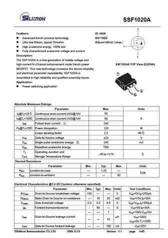
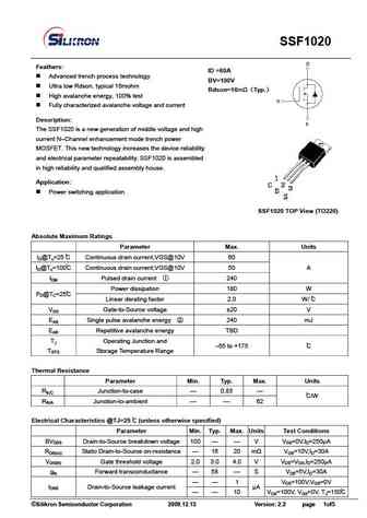
SSF1020A Feathers ID =60A Advanced trench process technology BV=100V Ultra low Rdson, typical 16mohm Rdson=20m max. High avalanche energy, 100% test Fully characterized avalanche voltage and current Description The SSF1020A is a new generation of middle voltage and high current N Channel enhancement mode trench power SSF1020A TOP View (D2PAK) MOSFET. This ne... See More ⇒
7.1. Size:458K silikron
ssf1020.pdf
SSF1020 Feathers ID =60A Advanced trench process technology BV=100V Ultra low Rdson, typical 16mohm Rdson=16m Typ. High avalanche energy, 100% test Fully characterized avalanche voltage and current Description The SSF1020 is a new generation of middle voltage and high current N Channel enhancement mode trench power MOSFET. This new technology i... See More ⇒
7.2. Size:685K silikron
ssf1020d.pdf
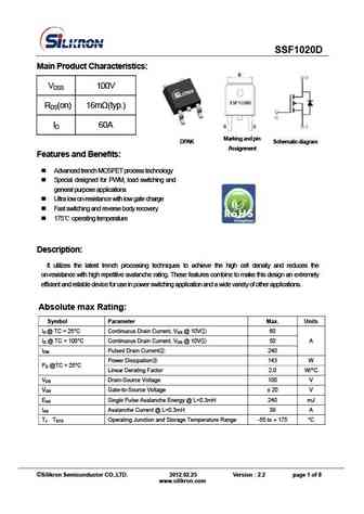
SSF1020D Main Product Characteristics VDSS 100V RDS(on) 16m (typ.) ID 60A DPAK Ma rk in g an d pi n Sc h ema t ic diag r am Assignment Features and Benefits Advanced trench MOSFET process technology Special designed for PWM, load switching and general purpose applications Ultra low on-resistance with low gate charge Fast switching and reverse body re... See More ⇒
9.1. Size:255K fairchild semi
ssf10n60a.pdf
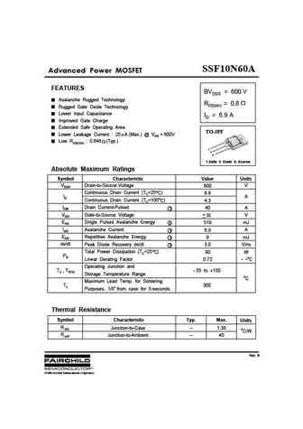
SSF10N60A Advanced Power MOSFET FEATURES BVDSS = 600 V Avalanche Rugged Technology RDS(on) = 0.8 Rugged Gate Oxide Technology Lower Input Capacitance ID = 6.9 A Improved Gate Charge Extended Safe Operating Area TO-3PF Lower Leakage Current 25 A (Max.) @ VDS = 600V Low RDS(ON) 0.646 (Typ.) 1 2 3 1.Gate 2. Drain 3. Source Absolute Maximum Ratings Symbol... See More ⇒
9.2. Size:577K samsung
ssf10n80a.pdf
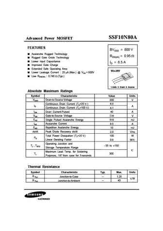
Advanced Power MOSFET FEATURES BVDSS = 800 V Avalanche Rugged Technology RDS(on) = 0.95 Rugged Gate Oxide Technology Lower Input Capacitance ID = 6.5 A Improved Gate Charge Extended Safe Operating Area Lower Leakage Current 25 A (Max.) @ VDS = 800V Low RDS(ON) 0.746 (Typ.) 1 2 3 1.Gate 2. Drain 3. Source Absolute Maximum Ratings Symbol Characteristic Val... See More ⇒
9.3. Size:579K samsung
ssf10n90a.pdf
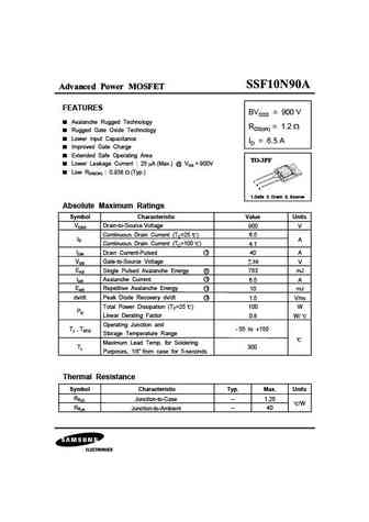
Advanced Power MOSFET FEATURES BVDSS = 900 V Avalanche Rugged Technology RDS(on) = 1.2 Rugged Gate Oxide Technology Lower Input Capacitance ID = 6.5 A Improved Gate Charge Extended Safe Operating Area Lower Leakage Current 25 A (Max.) @ VDS = 900V Low RDS(ON) 0.938 (Typ.) 1 2 3 1.Gate 2. Drain 3. Source Absolute Maximum Ratings Symbol Characteristic Valu... See More ⇒
9.5. Size:851K silikron
ssf1016d.pdf
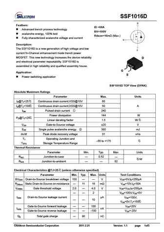
SSF1016D Feathers ID =60A Advanced trench process technology BV=100V avalanche energy, 100% test Rdson=16m (Max.) Fully characterized avalanche voltage and current Description The SSF1016D is a new generation of high voltage and low current N Channel enhancement mode trench power MOSFET. This new technology increases the device reliability and electrical par... See More ⇒
9.6. Size:659K silikron
ssf1009.pdf
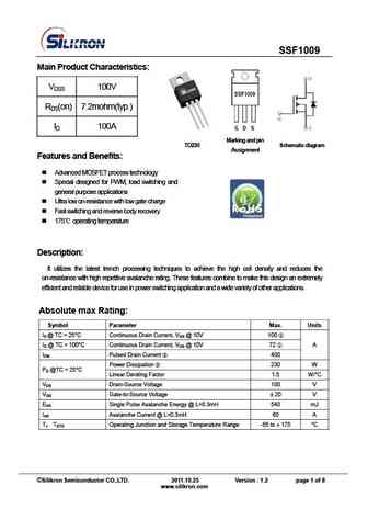
SSF1009 Main Product Characteristics VDSS 100V RDS(on) 7.2mohm(typ.) ID 100A Ma r k ing an d pin Sche ma ti c di agr a m TO220 Assignment Features and Benefits Advanced MOSFET process technology Special designed for PWM, load switching and general purpose applications Ultra low on-resistance with low gate charge Fast switching and reverse body rec... See More ⇒
9.7. Size:826K silikron
ssf1030d.pdf
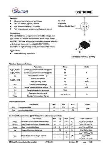
SSF1030D Feathers ID =45A Advanced trench process technology BV=100V Ultra low Rdson, typical 23mohm Rdson=23m typ. High avalanche energy, 100% test Fully characterized avalanche voltage and current Description The SSF1030D is a new generation of middle voltage and high current N Channel enhancement mode trench power MOSFET. This new technology increa... See More ⇒
9.8. Size:417K silikron
ssf1010.pdf
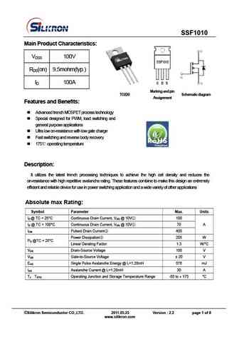
SSF1010 Main Product Characteristics VDSS 100V RDS(on) 9.5mohm(typ.) ID 100A Marking and pin TO220 Schematic diagram Assignment Features and Benefits Advanced trench MOSFET process technology Special designed for PWM, load switching and general purpose applications Ultra low on-resistance with low gate charge Fast switching and reverse body recovery 17... See More ⇒
9.9. Size:384K silikron
ssf1010a.pdf
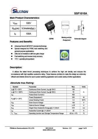
SSF1010A Main Product Characteristics VDSS 100V RDS(on) 9.5mohm(typ.) ID 100A Marking and pin D2PAK Schematic diagram Assignment Features and Benefits Advanced trench MOSFET process technology Special designed for PWM, load switching and general purpose applications Ultra low on-resistance with low gate charge Fast switching and reverse body recov... See More ⇒
9.10. Size:672K silikron
ssf1006.pdf
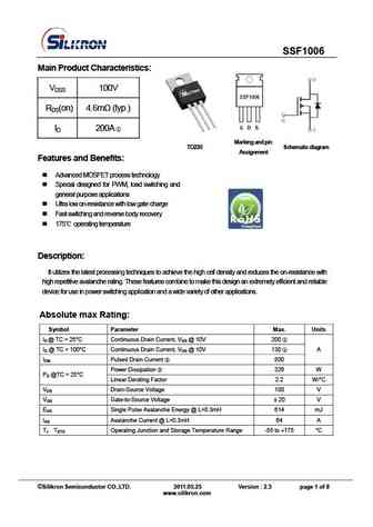
SSF1006 Main Product Characteristics VDSS 100V RDS(on) 4.6m (typ.) ID 200A Mar ki ng a nd p in Sche ma ti c di agr a m TO220 Assignment Features and Benefits Advanced MOSFET process technology Special designed for PWM, load switching and general purpose applications Ultra low on-resistance with low gate charge Fast switching and reverse body... See More ⇒
9.11. Size:536K silikron
ssf1030.pdf
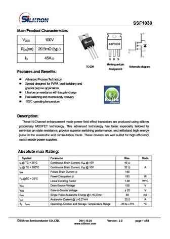
SSF1030 Main Product Characteristics VDSS 100V RDS(on) 20.5m (typ.) ID 45A Mar ki ng a nd p in Sche ma ti c di agr a m TO-220 Assignment Features and Benefits Advanced Process Technology Special designed for PWM, load switching and general purpose applications Ultra low on-resistance with low gate charge Fast switching and reverse body recov... See More ⇒
9.12. Size:716K silikron
ssf1090a.pdf
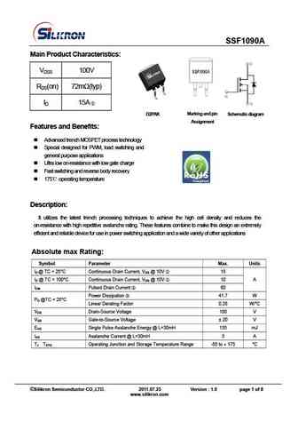
SSF1090A Main Product Characteristics VDSS 100V RDS(on) 72m (typ) ID 15A Marking and pin D2PAK Schematic diagram Assignment Features and Benefits Advanced trench MOSFET process technology Special designed for PWM, load switching and general purpose applications Ultra low on-resistance with low gate charge Fast switching and reverse body recovery ... See More ⇒
9.13. Size:921K silikron
ssf1006a.pdf
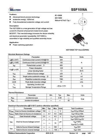
SSF1006A Feathers ID =200A Advanced trench process technology BV=100V avalanche energy, 100% test Rdson=4.7m Typ. Fully characterized avalanche voltage and current Description The SSF1006A is a new generation of high voltage and low current N Channel enhancement mode trench power MOSFET. This new technology increases the device reliability and electri... See More ⇒
9.14. Size:544K silikron
ssf1016a.pdf

SSF1016A Main Product Characteristics VDSS 100V RDS(on) 13.8mohm(typ.) ID 75A Marking and pin D2PAK Schematic diagram Assignment Features and Benefits Advanced trench MOSFET process technology Special designed for PWM, load switching and general purpose applications Ultra low on-resistance with low gate charge Fast switching and reverse body recover... See More ⇒
9.15. Size:731K silikron
ssf1016.pdf
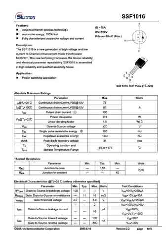
SSF1016 Feathers ID =75A Advanced trench process technology BV=100V avalanche energy, 100% test Rdson=16m (Max.) Fully characterized avalanche voltage and current Description The SSF1016 is a new generation of high voltage and low current N Channel enhancement mode trench power MOSFET. This new technology increases the device reliability and electrical ... See More ⇒
9.16. Size:390K silikron
ssf1030b.pdf
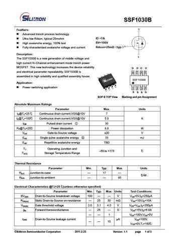
SSF1030B Feathers Advanced trench process technology ID =7A Ultra low Rdson, typical 25mohm BV=100V High avalanche energy, 100% test Rdson=25m typ. Fully characterized avalanche voltage and current Description The SSF1030B is a new generation of middle voltage and high current N Channel enhancement mode trench power MOSFET. This new technology ... See More ⇒
9.17. Size:410K silikron
ssf1007.pdf
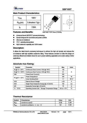
SSF1007 Main Product Characteristics VDSS 100V RDS(on) 5.8mohm Typ ID 130A Features and Benefits SSF1007 TOP View (TO220) Advanced trench MOSFET process technology Special designed for convertors and power controls Ultra low on-resistance 175 operating temperature High Avalanche capability and 100% tested Description It utilizes the latest trench... See More ⇒
9.19. Size:509K silikron
ssf1090.pdf
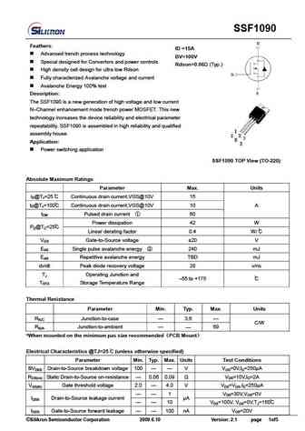
SSF1090 Feathers ID =15A Advanced trench process technology BV=100V Special designed for Convertors and power controls Rdson=0.06 (Typ.) High density cell design for ultra low Rdson Fully characterized Avalanche voltage and current Avalanche Energy 100% test Description The SSF1090 is a new generation of high voltage and low current N Channel en... See More ⇒
9.20. Size:464K silikron
ssf1006h.pdf
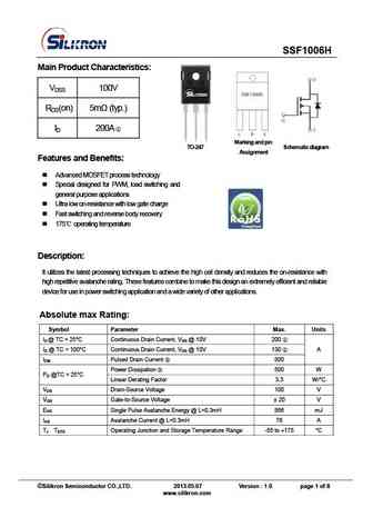
SSF1006H Main Product Characteristics VDSS 100V RDS(on) 5m (typ.) ID 200A Marking a nd p in TO-247 Schematic diagram Assignment Features and Benefits Advanced MOSFET process technology Special designed for PWM, load switching and general purpose applications Ultra low on-resistance with low gate charge Fast switching and reverse body recovery ... See More ⇒
9.22. Size:333K silikron
ssf10n90f1.pdf
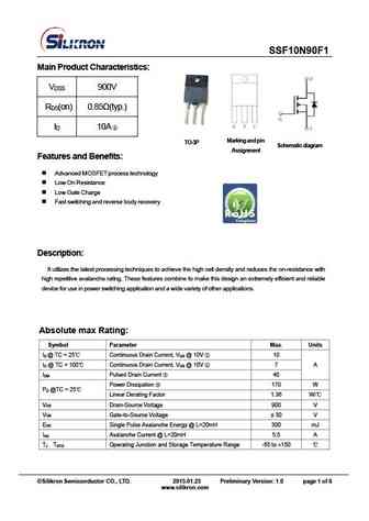
SSF10N90F1 Main Product Characteristics V 900V DSS R (on) 0.85 (typ.) DS I 10A D Marking and pin TO-3P Schematic diagram Assignment Features and Benefits Advanced MOSFET process technology Low On Resistance Low Gate Charge Fast switching and reverse body recovery Description It utilizes the latest processing techniques to achieve the high cell density a... See More ⇒
9.23. Size:436K silikron
ssf1090d.pdf

SSF1090D Main Product Characteristics VDSS 100V RDS(on) 60m (typ.) ID 15A TO-252 (D-PAK) Marking and pi n Sc he mat ic d ia gram Assignment Features and Benefits Advanced MOSFET process technology Special designed for PWM, load switching and general purpose applications Ultra low on-resistance with low gate charge Fast switching and reverse body... See More ⇒
Otros transistores... SSF1007
, SSF1009
, SSF1010
, SSF1010A
, SSF1016
, SSF1016A
, SSF1016D
, SSF1020
, 5N60
, SSF1020D
, SSF1030
, SSF1030B
, SSF1030D
, SSF1090
, SSF1090A
, SSF1090D
, SSF10N60
.
History: SL60N10Q