SSF3002EG1 MOSFET Equivalente. Reemplazo. Hoja de especificaciones. Principales características
Número de Parte: SSF3002EG1
Tipo de FET: MOSFET
Polaridad de transistor: N
ESPECIFICACIONES MÁXIMAS
Pdⓘ - Máxima disipación de potencia: 0.7 W
|Vds|ⓘ - Voltaje máximo drenador-fuente: 30 V
|Vgs|ⓘ - Voltaje máximo fuente-puerta: 20 V
|Id|ⓘ - Corriente continua de drenaje: 0.5 A
Tjⓘ - Temperatura máxima de unión: 150 °C
CARACTERÍSTICAS ELÉCTRICAS
trⓘ - Tiempo de subida: 45 nS
Cossⓘ - Capacitancia de salida: 18 pF
RDSonⓘ - Resistencia estado encendido drenaje a fuente: 1.5 Ohm
Encapsulados: SOT23
Búsqueda de reemplazo de SSF3002EG1 MOSFET
- Selecciónⓘ de transistores por parámetros
SSF3002EG1 datasheet
ssf3002eg1.pdf
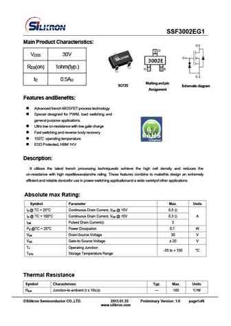
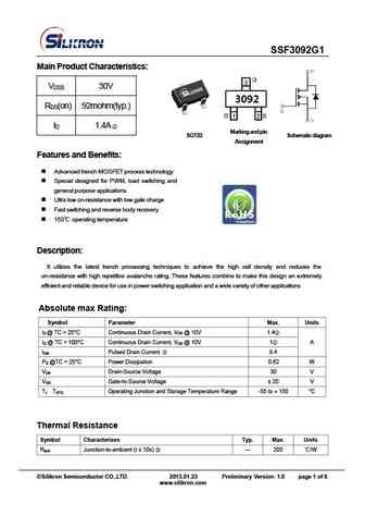
SSF3002EG1 Main Product Characteristics V 30V DSS R (on) 1ohm(typ.) DS I 0.5A D Marking and pin SOT23 Schematic diagram Assignment Features andBenefits Advanced trench MOSFET process technology Special designed for PWM, load switching and general purpose applications Ultra low on-resistance with low gate charge Fast switching and reverse body recovery 1
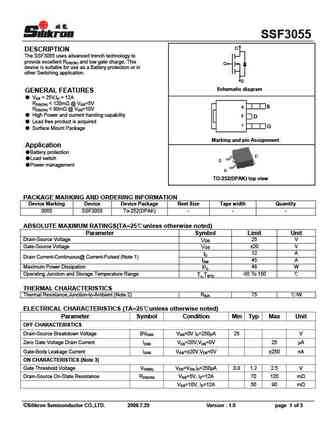
ssf3018.pdf
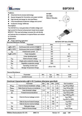
SSF3018 Feathers ID=60A Advanced trench process technology BV=100V Special designed for Convertors and power controls Rdson=15mohm High density cell design for ultra low Rdson Fully characterized Avalanche voltage and current Avalanche Energy 100% test Description The SSF3018 is a new generation of middle voltage and high current N Channel enhancement mode t
ssf3018d.pdf
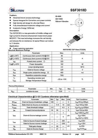
SSF3018D Feathers ID=80A Advanced trench process technology BV=100V Special designed for Convertors and power controls Rdson=14mohm High density cell design for ultra low Rdson Fully characterized Avalanche voltage and current Avalanche Energy 100% test Description The SSF3018D is a new generation of middle voltage and high current N Channel enhancement mod
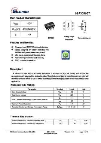
ssf3056c.pdf
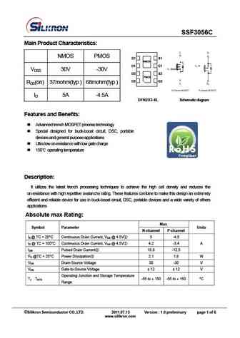
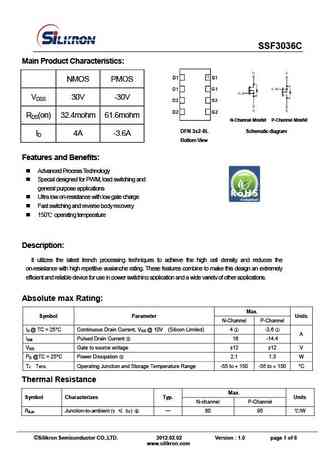
SSF3056C Main Product Characteristics NMOS PMOS D1 S1 D1 S1 NMOS NMOS D1 G1 D1 G1 VDSS 30V -30V D2 S2 D2 S2 PMOS PMOS D2 G2 D2 G2 RDS(on) 37mohm(typ.) 68mohm(typ.) ID 5A -4.5A DFN2X3-8L Schematic diagram Bottom View Features and Benefits Advanced trench MOSFET process technology Special designed for buck-boost circuit, DSC, portable devices and gene
Otros transistores... SSF2816E, SSF2816EB, SSF2841, SSF2N60, SSF2N60D, SSF2N60D2, SSF2N60F, SSF2N60G, 2SK3568, SSF3018, SSF3018D, SSF3028C1, SSF3036C, SSF3051G7, SSF3055, SSF3056C, SSF3092G1
🌐 : EN ES РУ

Liste
Recientemente añadidas las descripciónes de los transistores:
MOSFET: FTF30P35D | FTF25N35DHVT | FTF15N35D | FTE15C35G | FTP02P15G | FTE02P15G | AKF30N5P0SX | AKF30N10S | AKF20P45D | CM4407 | CM3407 | CM3400 | SVF11N65F | SVF11N65T | FKBB3105 | EHBA036R1
Popular searches
2sb649 | 2sb324 transistor | b754 transistor | 2sc828 equivalent | 4843ns | 2sc1318 datasheet | 2sc3281 datasheet | 2sa1106